

Page 1
Philips Semiconductors FAST Products Product specification
74F181Arithmetic logic unit
1
March 3, 1989 853–0351 95947
FEATURES
•Provides 16 arithmetic operation: add, subtract, compare, and
double; plus 12 other arithmetic operations
•Provides all 16 logic operations of two variables: Exclusive-OR,
Compare, AND, NAND, NOR, OR, plus 10 other logic operations
•Full look-ahead carry for high speed arithmetic operation on long
words
•40% faster than ’S181 with only 30% ’S181 power consumption
•Available in 300mil-wide Slim 24-pin Dual In-Line package
DESCRIPTION
The 74F181 is a 4-bit high-speed parallel Arithmetic Logic Unit
(ALU). Controlled by the four Function Select inputs (S0–S3) and
the Mode Control input (M), it can perform all the 16 possible logic
operations or 16 different arithmetic operations on active-High or
active-Low operands. The Function Table lists these operations.
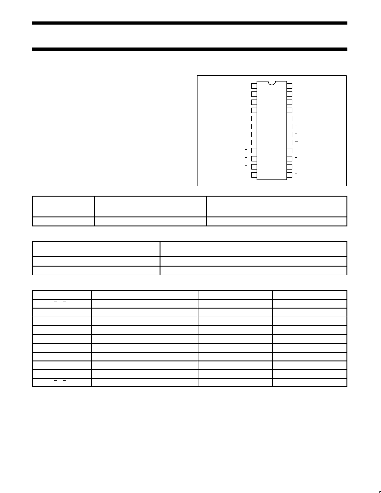
PIN CONFIGURATION
SF00193
1
2
3
4
5
6
7
8
9
10
11
12 13
14
15
16
17
18
19
20
21
22
23
24
B
0
A
0
S3
S2
S1
S0
Cn
M
F
0
F
1
F
2
V
CC
A1
B
1
A
2
B
2
A
3
B
3
C
n+4
G
P
A=B
F
3
GND
TYPE TYPICAL PROPAGATION DELAY
TYPICAL
SUPPLY CURRENT
(TOTAL)
74F181 7.0ns 43mA
ORDERING INFORMATION
DESCRIPTION
COMMERCIAL RANGE
V
CC
= 5V ±10%, T
amb
= 0°C to +70°C
24-Pin Plastic Slim DIP (300 mil) N74F181N
24-Pin Plastic SOL N74F181D
INPUT AND OUTPUT LOADING AND FAN-OUT TABLE
PINS DESCRIPTION 74F (U.L.) HIGH/LOW LOAD VALUE HIGH/LOW
A0–A3 A operand inputs 1.0/3.0 20µA/1.8mA
B0–B3 B operand inputs 1.0/3.0 20µA/1.8mA
M Mode control input 1.0/1.0 20µA/0.6mA
S0–S3 Function select input 1.0/4.0 20µA/2.4mA
Cn Carry input 1.0/5.0 20µA/3.0mA
C
n+4
Carry output 50/33 1.0mA/20mA
P Carry Propagate output 50/33 1.0mA/20mA
G Carry Generate output 50/33 1.0mA/20mA
A=B Compare output OC/33 OC/20mA
F0–F3 Outputs 50/33 1.0mA/20mA
NOTE: One (1.0) FAST unit load is defined as: 20µA in the High state and 0.6mA in the Low state.
OC = Open Collector
Page 2
Philips Semiconductors FAST Products Product specification
74F181Arithmetic logic unit
March 3, 1989
2
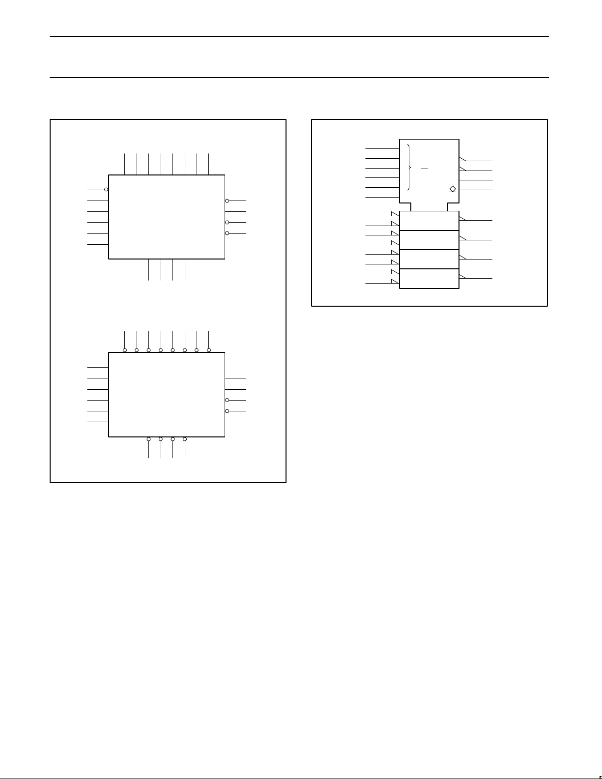
LOGIC SYMBOL
7
8
6
5
4
3
Cn
M
S0
S1
S2
S3
A0 B0 A1 B1 A2 B2 A3 B3
2 1 23 22 21 20 19 18
9 10 11 13
F0 F1 F2 F3
16
14
17
15
A=B
G
P
C
n+4
Active-High Operands
7
8
6
5
4
3
Cn
M
S0
S1
S2
S3
A0 B0 A1 B1 A2 B2 A3 B3
2 1 23 22 21 20 19 18
9 10 11 13
F0 F1 F2 F3
16
14
17
15
A=B
G
P
C
n+4
Active-Low Operands
VCC = Pin 24
GND = Pin 12
SF00196
IEC/IEEE SYMBOL
SF00197
0
1
2
3
5
6
ALU
[T]
P0
Q0
9
4
M
0
21
8
7
CI
4
17
15
16
14
CP
CG
CO
P=G
22
23
P1
Q1
10
20
21
P2
Q2
11
18
19
P3
Q3
13
Page 3
Philips Semiconductors FAST Products Product specification
74F181Arithmetic logic unit
March 3, 1989
3
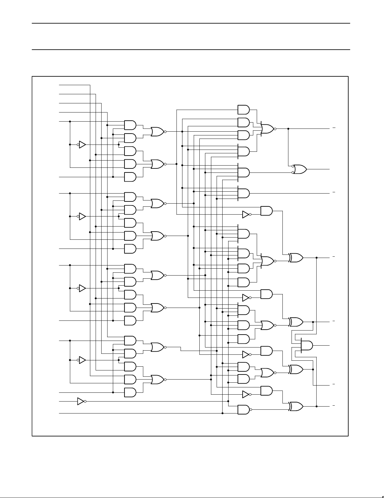
LOGIC DIAGRAM
S0
6
S1
5
S2
4
S3
B3
3
18
A3
19
B2
20
A2
21
A1
23
A0
2
M
8
7
B1
22
B0
1
Cn
V
CC
= Pin 24
GND = Pin 12
17
G
16
C
n+4
15
P
13
F
3
11
F
2
14
A=B
10
F
1
9
F
0
SF00194
Page 4
Philips Semiconductors FAST Products Product specification
74F181Arithmetic logic unit
March 3, 1989
4
When the Mode Control input (M) is High, all internal carries are
inhibited and the device performs logic operations on the individual
bits as listed. When the Mode control input is Low, the carries are
enabled and the device performs arithmetic operations on the two
4-bit words. The device incorporates full internal carry look-ahead
and provides for either ripple carry between device using the C
n+4
output, or for carry look-ahead between packages using the signals
P
(Carry Propagate) and G (Carry Generate). P and G are not
affected by carry in. When speed requirements are not stringent, it
can be used in a simple ripple carry mode by connecting the Carry
output (C
n+4
) signal to the Carry input (Cn) of the next unit. For
high-speed operation, the device is used in conjunction with the
74F182 carry look-ahead circuit. One carry look-ahead package is
required for each group of four 74F181 devices. Carry look-ahead
can be provided at various levels and offers high speed capability
over extremely long word lengths.
The A=B output from the device goes High when all four F outputs
are High and can be used to indicate logic equivalence over 4-bits
when the unit is in the subtract mode. The A=B output is
open-collector and can be wired-AND with other A=B outputs to give
a comparison for more than 4 bits. The A=B signal can also be used
with the C
n+4
signal to indicate A>B and A<B. The Function Table
lists the arithmetic operations that are performed without a carry in.
An incoming carry adds a one to each operation. Thus select code
LHHL generates A minus B minus 1 (two’s complement notation)
without a carry in and generates A minus B when a carry is applied.
Because subtraction is actually performed by complementary
addition (one’s complement), a carry out means borrow; thus, a
carry is generated when there is no underflow and no carry is
generated when there is underflow. As indicated, this device can be
used with either active-Low inputs producing active-Low outputs or
with active-High inputs producing active-High outputs. For either
case, the table lists the operations that are performed to the
operands labeled inside the logic symbol.
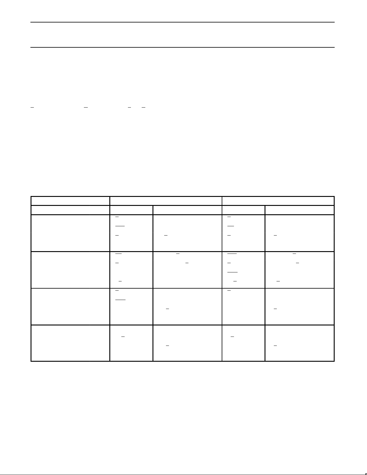
MODE-SELECT FUNCTION TABLE
MODE SELECT INPUTS ACTIVE HIGH INPUTS & OUTPUTS ACTIVE LOW INPUTS & OUTPUTS
S3 S2 S1 S0 Logic (M=H) Arithmetic** (M=L) (Cn=H) Logic (M=H) Arithmetic** (M=L) (Cn=L)
L L L L A A A A minus 1
L L L H A+B A+B AB AB minus 1
L L H L AB A+B A+B AB minus 1
L L H H Logical 0 minus 1 Logical 1 minus 1
L H L L AB A plus AB A+B A plus (A+B)
L H L H B (A+B) plus AB B AB plus (A+B)
L H H L A⊕B A minus B minus 1 A⊕B A minus B minus 1
L H H H AB AB minus 1 A+B A+B
H L L L A+B A plus AB AB A plus (A+B)
H L L H A⊕B A plus B A⊕B A plus B
H L H L B (A+B) plus AB B AB plus (A+B)
H L H H AB AB minus 1 A+B A+B
H H L L Logical 1 A plus A* Logical 0 A plus A*
H H L H A+B (A+B) plus A AB AB plus A
H H H L A+B (A+B) plus A AB AB plus A
H H H H A A minus 1 A A
H = High voltage level
L = Low voltage level
* = Each bit is shifted to the next more significant position.
** = Arithmetic operations expressed in two’s complement notation.
Page 5
Philips Semiconductors FAST Products Product specification
74F181Arithmetic logic unit
March 3, 1989
5
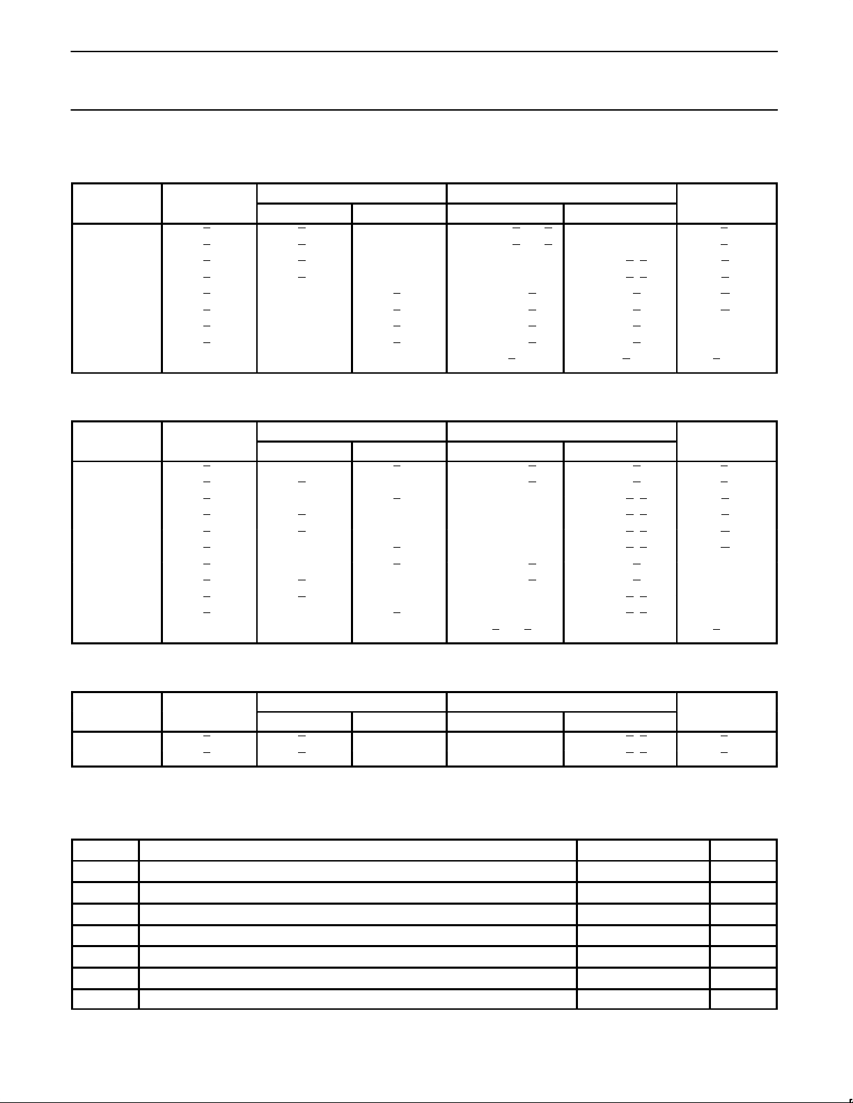
Table 1. Sum Mode Test
Function Inputs: S0 = S3 = 4.5V, S1 = S2 = M = 0V
INPUT
OTHER INPUT, SAME BIT OTHER DATA INPUTS
OUTPUT
PARAMETER
INPUT
UNDER TEST
Apply 4.5V Apply GND Apply 4.5V Apply GND
OUTPUT
UNDER TEST
t
PLH
, t
PHL
A
i
B
i
None Remaining A and B Cn F
i
t
PLH
, t
PHL
B
i
A
i
None Remaining A and B Cn F
i
t
PLH
, t
PHL
A
i
B
i
None None Remaining A, B, Cn P
t
PLH
, t
PHL
B
i
A
i
None None Remaining A, B, Cn P
t
PLH
, t
PHL
A
i
None B
i
Remaining B Remaining A, Cn G
t
PLH
, t
PHL
B
i
None A
i
Remaining B Remaining A, Cn G
t
PLH
, t
PHL
A
i
None B
i
Remaining B Remaining A, Cn C
n+4
t
PLH
, t
PHL
B
i
None A
i
Remaining B Remaining A, Cn C
n+4
t
PLH
, t
PHL
Cn None None All A All B Any F or C
n+4
Table 2. Diff Mode Test
Function Inputs: S1 = S2 = 4.5V, S0 = S3 = M = 0V
INPUT
OTHER INPUT, SAME BIT OTHER DATA INPUTS
OUTPUT
PARAMETER
INPUT
UNDER TEST
Apply 4.5V Apply GND Apply 4.5V Apply GND
OUTPUT
UNDER TEST
t
PLH
, t
PHL
A
i
None B
i
Remaining A Remaining B, Cn F
i
t
PLH
, t
PHL
B
i
A
i
None Remaining A Remaining B, Cn F
i
t
PLH
, t
PHL
A
i
None B
i
None Remaining A, B, Cn P
t
PLH
, t
PHL
B
i
A
i
None None Remaining A, B, Cn P
t
PLH
, t
PHL
A
i
B
i
None None Remaining A, B, Cn G
t
PLH
, t
PHL
B
i
None A
i
None Remaining A, B, Cn G
t
PLH
, t
PHL
A
i
None B
i
Remaining A Remaining B, Cn A=B
t
PLH
, t
PHL
B
i
A
i
None Remaining A Remaining B, Cn A=B
t
PLH
, t
PHL
A
i
B
i
None None Remaining A, B, Cn C
n+4
t
PLH
, t
PHL
B
i
None A
i
None Remaining A, B, Cn C
n+4
t
PLH
, t
PHL
Cn None None All A and B None Any F or C
n+4
Table 3. Logic Mode Test
Function Inputs: S1 = S2 = 4.5V, S0 = S3 = 0V
INPUT
OTHER INPUT, SAME BIT OTHER DATA INPUTS
OUTPUT
PARAMETER
INPUT
UNDER TEST
Apply 4.5V Apply GND Apply 4.5V Apply GND
OUTPUT
UNDER TEST
t
PLH
, t
PHL
A
i
B
i
None None Remaining A, B, Cn F
i
t
PLH
, t
PHL
B
i
A
i
None None Remaining A, B, Cn F
i
ABSOLUTE MAXIMUM RATINGS
(Operation beyond the limits set forth in this table may impair the useful life of the device.
Unless otherwise noted these limits are over the operating free-air temperature range.)
SYMBOL
PARAMETER RATING UNIT
V
CC
Supply voltage –0.5 to +7.0 V
V
IN
Input voltage –0.5 to +7.0 V
I
IN
Input current –30 to +5 mA
V
OUT
Voltage applied to output in High output state –0.5 to V
CC
V
I
OUT
Current applied to output in Low output state 40 mA
T
amb
Operating free-air temperature range 0 to +70 °C
T
stg
Storage temperature range –65 to +150 °C
Page 6
Philips Semiconductors FAST Products Product specification
74F181Arithmetic logic unit
March 3, 1989
6
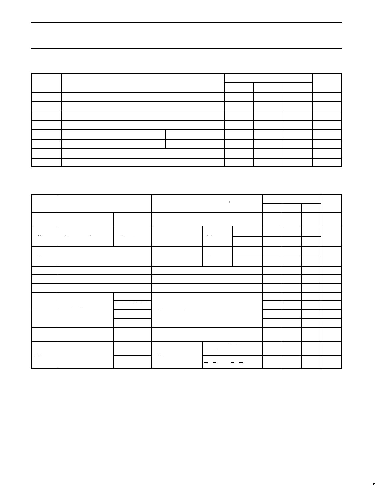
RECOMMENDED OPERATING CONDITIONS
LIMITS
SYMBOL
PARAMETER
MIN NOM MAX
UNIT
V
CC
Supply voltage 4.5 5.0 5.5 V
V
IH
High-level input voltage 2.0 V
V
IL
Low-level input voltage 0.8 V
I
IK
Input clamp current –18 mA
V
OH
High level output voltage A=B only 4.5 V
I
OH
High-level output current Any output except A=B –1 mA
I
OL
Low-level output current 20 mA
T
amb
Operating free-air temperature range 0 +70 °C
DC ELECTRICAL CHARACTERISTICS
(Over recommended operating free-air temperature range unless otherwise noted.)
LIMITS
SYMBOL
PARAMETER
TEST CONDITIONS
1
MIN TYP2MAX
UNIT
I
OH
High-level output
current
A=B only VCC = MIN, VIL = MAX; VIH = MIN, VOH = MAX 250 µA
±10%V
CC
2.5
V
OH
High-level output
voltage
Any output
except A=B
VIL = MAX,
VIH = MIN
IOH = MAX
±5%V
CC
2.7 3.4
V
±10%V
CC
0.30 0.50
VOLLow-level output voltage
VIL = MAX,
VIH = MIN
IOL = MAX
±5%V
CC
0.30 0.50
V
V
IK
Input clamp voltage VCC = MIN, II = I
IK
–0.73 –1.2 V
I
I
Input current at maximum input voltage VCC = MAX, VI = 7.0V 100 µA
I
IH
High-level input current VCC = MAX, VI = 2.7V 20 µA
M
–0.6 mA
A0–A3, B0–B3
–1.8 mA
IILLow-level input current
S0–S3
VCC = MAX, VI = 0.5V
–2.4 mA
Cn –3.0 mA
I
OS
Short-circuit output
current
3
Any output
except A=B
VCC = MAX –60 –150 mA
I
CCH
S0–S3=M=A0–A3=4.5V,
B
0–B3=Cn=GND
43 65 mA
ICCSupply current (total)
I
CCL
VCC = MAX
S0–S3=M=4.5V,
B
0–B3=Cn=A0–A3=GND
43 65 mA
NOTES:
1. For conditions shown as MIN or MAX, use the appropriate value specified under recommended operating conditions for the applicable type.
2. All typical values are at V
CC
= 5V, T
amb
= 25°C.
3. Not more than one output should be shorted at a time. For testing I
OS
, the use of high-speed test apparatus and/or sample-and-hold
techniques are preferable in order to minimize internal heating and more accurately reflect operational values. Otherwise, prolonged shorting
of a High output may raise the chip temperature well above normal and thereby cause invalid readings in other parameter tests. In any
sequence of parameter tests, I
OS
tests should be performed last.
High-level output
Any output
VCC = MIN,
VCC = MIN,
Page 7
Philips Semiconductors FAST Products Product specification
74F181Arithmetic logic unit
March 3, 1989
7
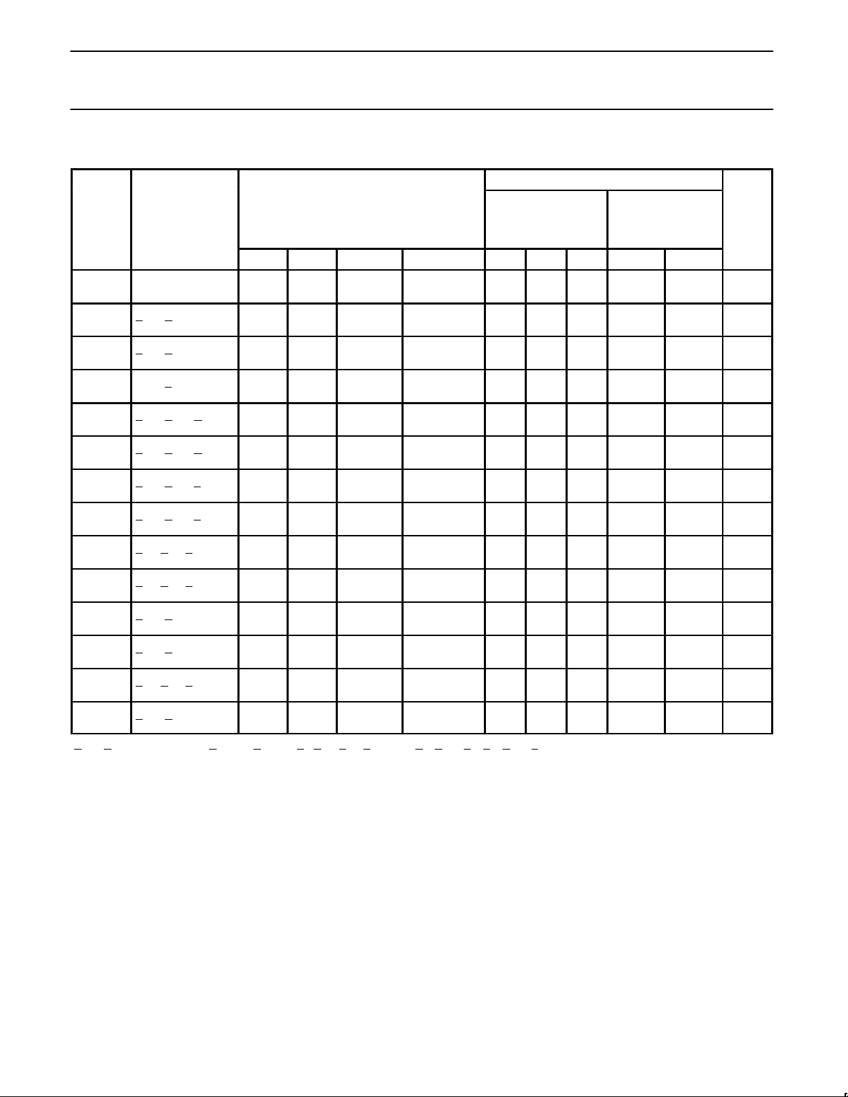
AC ELECTRICAL CHARACTERISTICS
LIMITS
SYMBOL
PARAMETER
TEST CONDITIONS
VCC = +5.0V
T
amb
= +25°C
CL = 50pF
R
L
= 500Ω
VCC = +5.0V ± 10%
T
amb
= 0°C to +70°C
CL = 50pF
R
L
= 500Ω
UNIT
Mode Table Waveform Condition MIN TYP MAX MIN MAX
t
PLH
t
PHL
Propagation delay
Cn to C
n+4
Sum
Diff
1
2
1 M=0V 3.0
2.5
5.0
5.0
8.0
8.0
3.0
2.5
8.5
8.5
ns
t
PLH
t
PHL
Propagation delay
A
n or Bn to C
n+4
Sum 1 2 M=S1=S2=0V,
S0=S3=4.5V
5.0
5.0
9.0
8.0
12.0
12.0
5.0
5.0
13.0
12.5
ns
t
PLH
t
PHL
Propagation delay
A
n or Bn to C
n+4
Diff 2 2 M=S0=S3=0V,
S1=S2=4.5V
5.0
5.0
9.5
8.0
13.0
12.0
5.0
5.0
14.0
12.5
ns
t
PLH
t
PHL
Propagation delay
Cn to F
n
Diff
Sum
2
1
1 M=0V 3.0
3.0
5.0
5.0
8.0
8.0
3.0
2.5
9.0
9.0
ns
t
PLH
t
PHL
Propagation delay
A
n or Bn to G
Sum 1 1 M=S1=S2=0V,
S0=S3=4.5V
3.0
3.0
5.0
5.0
7.5
7.5
2.5
2.5
8.0
8.0
ns
t
PLH
t
PHL
Propagation delay
A
n or Bn to G
Diff 2 2 M=S0=S3=0V,
S1=S2=4.5V
3.0
3.0
4.5
5.0
8.0
8.5
2.5
2.5
9.0
9.5
ns
t
PLH
t
PHL
Propagation delay
A
n or Bn to P
Sum 1 2 M=S1=S2=0V,
S0=S3=4.5V
2.5
3.0
4.0
4.5
7.0
7.5
2.0
2.5
7.5
8.0
ns
t
PLH
t
PHL
Propagation delay
A
n or Bn to P
Diff 2 1, 2 M=S0=S3=0V,
S1=S2=4.5V
2.5
3.0
4.0
5.0
7.5
8.5
2.0
2.5
8.0
9.0
ns
t
PLH
t
PHL
Propagation delay
A
i
or Bi to F
i
Sum 1 1, 2 M=S1=S2=0V,
S0=S3=4.5V
3.0
3.0
4.5
4.5
7.5
7.5
2.5
3.0
8.5
8.5
ns
t
PLH
t
PHL
Propagation delay
A
i
or Bi to F
i
Diff 2 1, 2 M=S0=S3=0V,
S1=S2=4.5V
3.0
3.0
4.5
5.0
8.5
8.5
2.5
3.0
9.0
9.0
ns
t
PLH
t
PHL
Propagation delay
A
n or Bn to Fn
Sum 1, 2 3.5
3.5
6.0
5.5
10.0
9.5
3.0
3.0
11.0
10.0
ns
t
PLH
t
PHL
Propagation delay
A
n or Bn to Fn
Diff 1, 2 4.0
4.5
6.5
7.0
10.5
10.5
3.5
4.5
11.0
11.0
ns
t
PLH
t
PHL
Propagation delay
A
i
or Bi to F
i
Logic 3 1, 2 M=4.5V 3.5
3.5
5.5
5.5
9.0
10.0
3.0
3.0
9.5
10.5
ns
t
PLH
t
PHL
Propagation delay
A
n or Bn to A=B
Diff 2 1, 2 M=S0=S3=0V,
S1=S2=4.5V
10.0
6.0
14.0
8.5
19.0
12.5
9.5
5.5
20.5
12.5
ns
NOTES:
“An or Bn to Fn” means any A or any B to any F; “Ai or Bi to Fi” means A1, B1 to F1; A2, B2 to F2 (the identifying number must be the same).
Page 8
Philips Semiconductors FAST Products Product specification
74F181Arithmetic logic unit
March 3, 1989
8
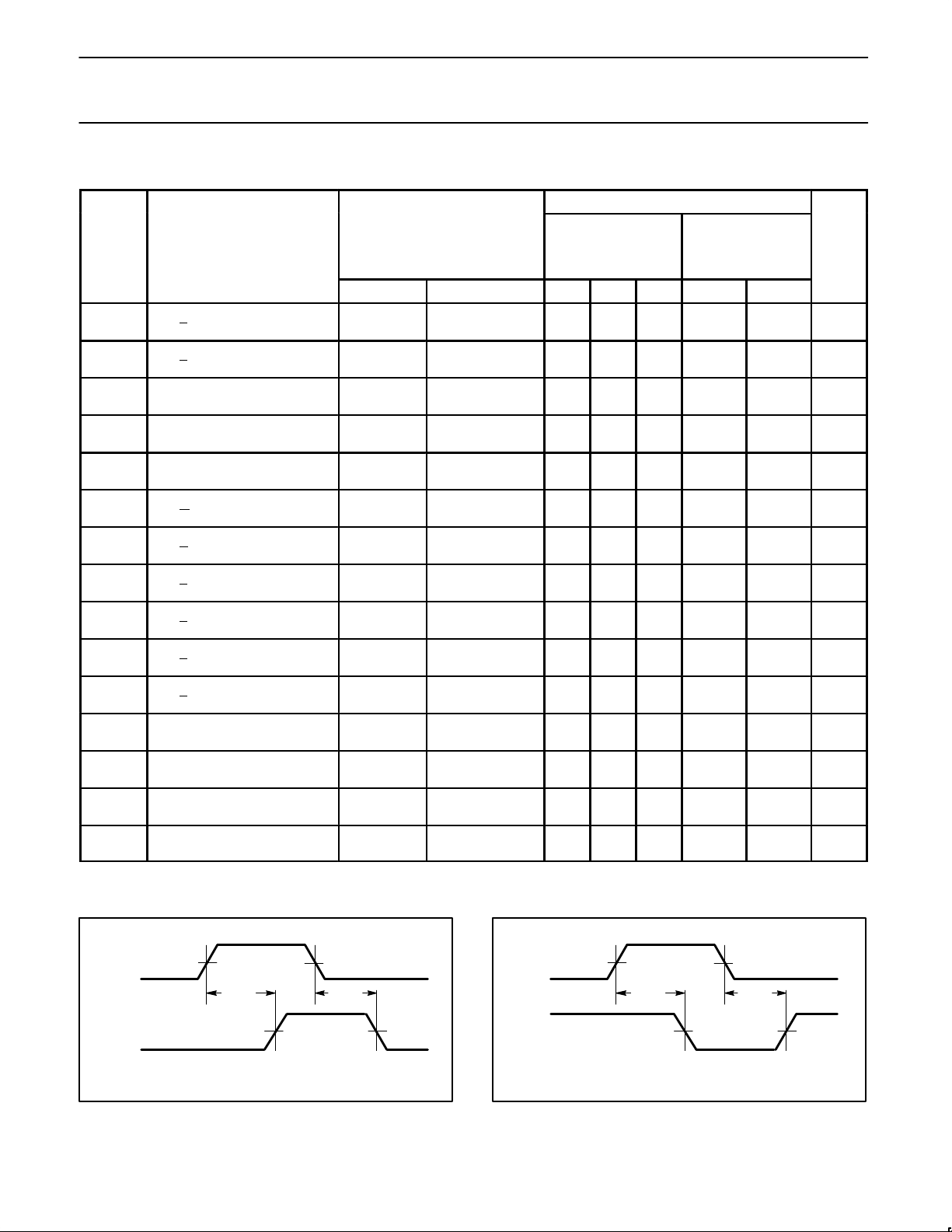
AC ELECTRICAL CHARACTERISTICS
LIMITS
SYMBOL
PARAMETER
TEST CONDITIONS
VCC = +5.0V
T
amb
= +25°C
CL = 50pF
R
L
= 500Ω
VCC = +5.0V ± 10%
T
amb
= 0°C to +70°C
CL = 50pF
R
L
= 500Ω
UNIT
Mode Waveform MIN TYP MAX MIN MAX
t
PLH
t
PHL
Propagation delay
Si to Fi (Inverting)
1 3.5
3.5
5.5
5.0
8.0
8.0
3.0
3.0
9.0
9.0
ns
t
PLH
t
PHL
Propagation delay
S
i
to Fi (Non-Inverting)
2 3.0
3.0
5.5
5.5
8.5
8.5
3.0
3.0
9.5
9.5
ns
t
PLH
t
PHL
Propagation delay
S
i
to A=B (Inverting)
1 10.5
6.0
16.5
8.0
22.5
11.0
10.5
6.0
24.0
11.5
ns
t
PLH
t
PHL
Propagation delay
S
i
to A=B (Non-Inverting)
2 10.0
5.5
15.0
8.5
19.0
12.5
10.0
5.0
21.0
13.5
ns
t
PLH
t
PHL
Propagation delay
S
i
to C
n+4
(Inverting)
1 3.5
3.0
7.0
5.5
11.0
10.0
3.0
2.5
12.5
10.0
ns
t
PLH
t
PHL
Propagation delay
S
i
to G (Non-Inverting)
2 2.5
2.5
5.0
4.0
7.5
7.5
2.5
2.5
8.0
8.0
ns
t
PLH
t
PHL
Propagation delay
S
i
to P (Non-Inverting)
2 2.5
2.5
4.0
4.5
6.5
7.0
2.5
2.5
7.0
8.0
ns
t
PLH
t
PHL
Propagation delay
M to F
i
(Inverting)
Sum 1 3.5
3.5
6.0
6.0
8.5
8.5
3.5
3.5
9.5
9.5
ns
t
PLH
t
PHL
Propagation delay
M to F
i
(Non-Inverting)
Sum 2 4.5
4.0
7.0
6.0
10.0
9.5
4.5
4.0
11.0
10.0
ns
t
PLH
t
PHL
Propagation delay
M to F
i
(Inverting)
Diff 1 3.5
3.5
6.0
6.0
8.5
8.5
3.5
3.5
9.5
9.5
ns
t
PLH
t
PHL
Propagation delay
M to F
i
(Non-Inverting)
Diff 2 4.0
4.0
7.0
6.0
10.0
9.5
4.0
4.0
11.5
10.0
ns
t
PLH
t
PHL
Propagation delay
M to A=B (Inverting)
Sum 1 12.0
6.5
16.0
8.0
20.0
11.0
11.0
6.0
22.0
11.0
ns
t
PLH
t
PHL
Propagation delay
M to A=B (Non-Inverting)
Sum 2 13.0
6.5
17.0
8.0
21.0
10.5
12.0
6.0
24.0
11.5
ns
t
PLH
t
PHL
Propagation delay
M to A=B (Inverting)
Diff 1 11.5
6.0
16.0
8.0
20.0
10.5
10.5
6.0
22.0
11.0
ns
t
PLH
t
PHL
Propagation delay
M to A=B (Non-Inverting)
Diff 2 13.0
6.0
17.0
8.0
21.5
11.0
12.5
6.0
24.0
11.5
ns
AC WAVEFORMS
For all waveforms, VM = 1.5V.
V
M
V
M
V
M
V
M
V
OUT
V
IN
t
PLH
t
PHL
SF00092
Waveform 1. Propagation Delay for Non-Inverting Paths
V
M
V
M
V
M
V
M
V
OUT
V
IN
t
PHL
t
PLH
SF00093
Waveform 2. Propagation Delay for Inverting Paths
Page 9
Philips Semiconductors FAST Products Product specification
74F181Arithmetic logic unit
March 3, 1989
9
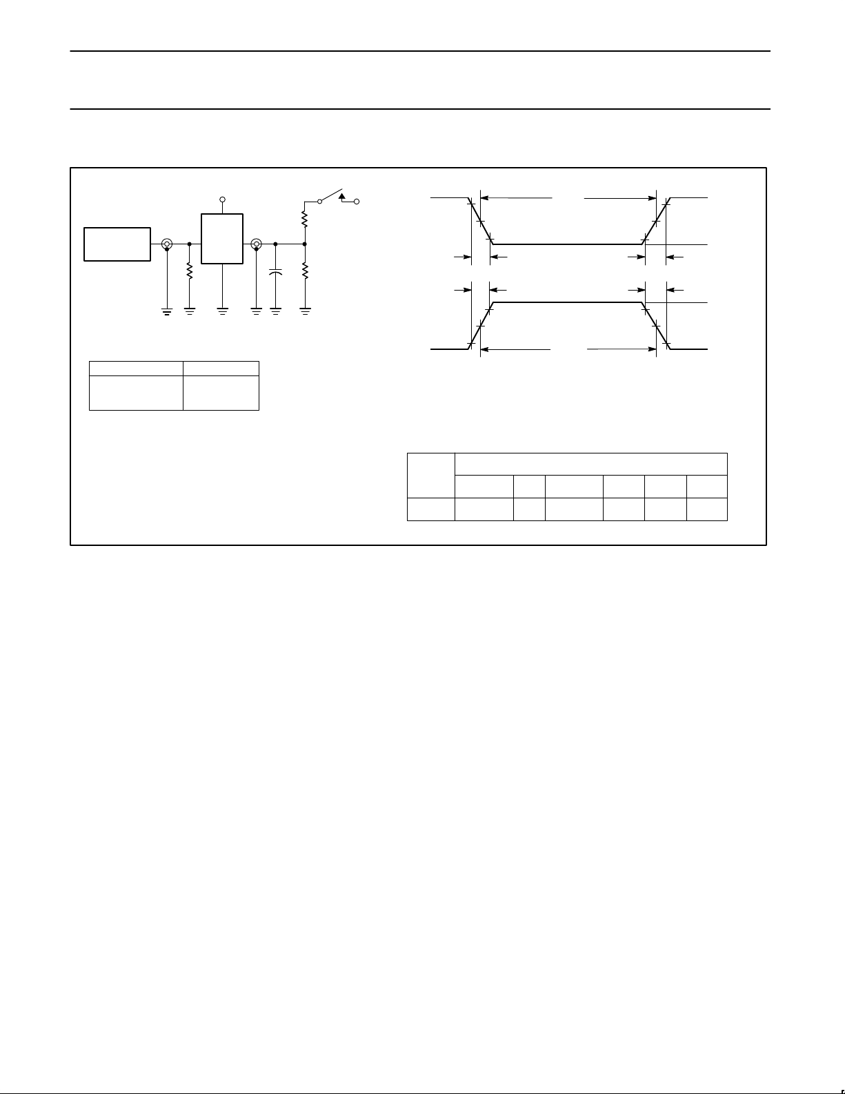
TEST CIRCUIT AND WAVEFORMS
t
w
90%
V
M
10%
90%
V
M
10%
90%
V
M
10%
90%
V
M
10%
NEGATIVE
PULSE
POSITIVE
PULSE
t
w
AMP (V)
0V
0V
t
THL (tf
)
INPUT PULSE REQUIREMENTS
rep. rate
t
w
t
TLH
t
THL
1MHz 500ns
2.5ns 2.5ns
Input Pulse Definition
V
CC
family
74F
D.U.T.
PULSE
GENERATOR
R
L
C
L
R
T
V
IN
V
OUT
Test Circuit for Open Collector Outputs
DEFINITIONS:
R
L
= Load resistor;
see AC electrical characteristics for value.
CL= Load capacitance includes jig and probe capacitance;
see AC electrical characteristics for value.
RT= Termination resistance should be equal to Z
OUT
of
pulse generators.
t
THL (tf
)
t
TLH (tr
)
t
TLH (tr
)
AMP (V)
amplitude
3.0V 1.5V
V
M
R
L
7.0V
SF00195
TEST SWITCH
Open Collector closed
All other open
SWITCH POSITION
 Loading...