

Page 1
Preliminary
SERIAL PORTS
USER INTERFACE
EP9312 Product Overview
FEATURES
■ 200MHz ARM920T Processor
— 16kbyte Instruction Cache
— 16kbyte Data Cache
— Windows CE enabled MMU
■ MaverickCrunch
— Floating point, integer and signal processing
instructions
— Optimized for digital music compression and
decompression algorithms
— Hardware interlocks allow in-line coding
■ MaverickLock
— Incorporates boot ROM, laser fuses, and
gate-level IP
— Multiple security vendors can co-exist in same
system
— Exceeds SDMI requirements
™
Math Engine
Security Features
Internet Audio Jukebox Processor
with MaverickCrunch™ Audio
Compression and MaverickLock™
Security
OVERVIEW
The EP9312 is an ARM920T based system on chip
designed for use in audio jukebox applications where
processor performance, signal processing capability,
communications bandwidth, storage capabilities, and the
user interface are properly balanced to provide up to 4
streams of compressed audio data (MP3, WMA, and
other audio compression standards) through a home
network.
(Cont.)(Cont.)
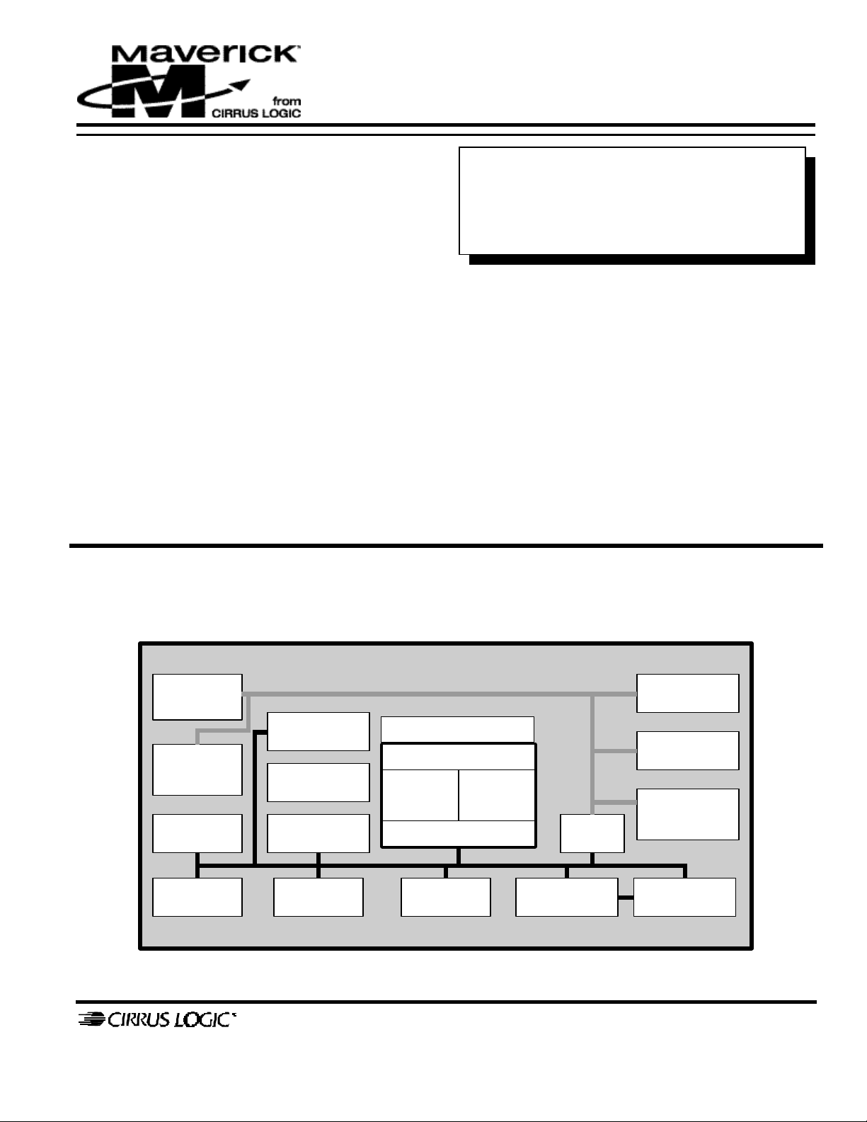
BLOCK DIAGRAM
Serial
Audio
Interface
(3) UARTs
w/
IRDA
(3) USB
Hosts
Ethernet
MAC
DMA w/
CRC
MaverickLock
Boot
ROM
EIDE
I/F
TM
MEMORY AND STORAGE
Peripheral Bus
MaverickCrunch
ARM920T
D-Cache
16KB
I-Cache
16KB
MMU
SRAM &
Flash I/F
TM
Bus
Bridge
Unified
SDRAM I/F
Clocks &
Timers
Interrupts
& GPIO
Keypad &
Touch
Screen I/F
Processor Bus
Video/LCD
Controller
P.O. Box 17847, Austin, Texas 78760
(512) 445 7222 FAX: (512) 445 7581
http://www.cirrus.com
Copyright 2001 Cirrus Logic (All Rights Reserved) Jan’01
DS515PO3
1
Page 2

EP9312
Internet Audio Jukebox Processor Preliminary
FEATURES (cont.)
■ Integrated Peripheral Interfaces
— EIDE (up to 2 devices)
— 1/10/100Mbps Ethernet MAC
— Three 16550 compatible UARTs
— Three-port USB Host
— IRDA Interface
— 32-bit SDRAM Interface up to 4 banks
— 32/16-bit SRAM/FLASH/ROM
— EEPROM Interface
OVERVIEW (cont.)
The ARM920T microprocessor core with separate
16Kbyte, 64-way set-associative instruction and data
caches is augmented by the MaverickCrunch™ coprocessor enabling faster than real-time compression of
audio CDs. The proprietary MaverickLock™ technology
exceeds security requirements set forth by SDMI to
protect music content. It may also be used to protect
proprietary firmware, transactions, and other digital
content.
A high-performance 1/10/100Mbps Ethernet Media
Access Controller (EMAC) is included along with
■ Internal Peripherals
— Real-time Clock with software Trim
— Eight Direct Memory Access (DMA) Channels
with Cyclic Redundancy Check (CRC) Generation
— Dual PLL controls all clock domains
— Watchdog Timer
— Interrupt Controller
— Four general purpose 16-bit timers
— 40-bit Debug Timer
— Boot ROM
■ Package
— 352 pin PBGA
2
external interfaces to SPI and I
S audio, LCD, IDE
storage peripherals, keypad, and touchscreen. A threeport USB host and three UARTs are included as well.
The EP9213 is a high-performance, low-power RISCbased single-chip computer built around an ARM920T
microprocessor core with a maximum operating clock
rate of 200MHz. The ARM core is operateS from a 2.5V
supply, while the I/O operates at 3.3V with power
between 350mW and 1000mW dependent on speed.
Contacting Cirrus Logic Support
For a complete listing of Direct Sales, Distributor, and Sales Representative contacts, visit the Cirrus Logic web site at:
http://www.cirrus.com/corporate/contacts/
Preliminary product information describes products which are in production, but for which full characterization data is not yet available. Advance product information
describes products which are in development and subject to development changes. Cirrus Logic, Inc. has made best efforts to ensu re that the information contained in this
document is accurate and reliable. However, the information is subject to change without notice and is provided “AS IS” without warranty of any kind (express or implied).
No responsibility is assumed by Cirrus Logic, Inc. for the use of this information, nor for infringements of patents or other rights of third parties. This document is the
property of Cirrus Logic, Inc. and implies no license under patents, copyrights, trademarks, or trade secrets. No part of this p ublication may be copied, reproduced, stored
in a retrieval system, or transmitted, in any form or by any means (electronic, mechanical, photographic, or otherwise) without the prior written consent of Cirrus Logic, Inc.
Items from any Cirrus Logic website or disk may be printed for use by the user. However, no part of the printout or electronic files may be copied, reproduced, stored in a
retrieval system, or transmitted, in any form or by any means (electronic, mechanical, photographic, or otherwise) without the p rior written consent of Cirrus Logic,
Inc.Furthermore, no part of this publication may be used as a basis for manufacture or sale of any items without the prior written consent of Cirrus Logic, Inc. The names of
products of Cirrus Logic, Inc. or other vendors and suppliers appearing in this document may be trademarks or service marks of their respective owners which may be
registered in some jurisdictions. A list of Cirrus Logic, Inc. trademarks and service marks can be found at http://www.cirrus.co m.
2 Copyright 2001 Cirrus Logic (All Rights Reserved) DS515PO3
Page 3

EP9312
Preliminary Internet Audio Jukebox Processor
Processor Core - ARM920T
The ARM920T is a Harvard architecture processor with
separate 16Kbyte instruction and data caches with an 8word line length. The processor utilizes a five-stage
pipeline consisting of fetch, decode, execute, memory
and write stages. Key features include:
• ARM (32-bit) and Thumb (16-bit compressed)
instruction sets
• 32-bit Advanced Micro-Controller Bus
Architecture (AMBA)
• 16Kbyte Instruction Cache with lockdown
• 16Kbyte Data Cache (programmable writethrough or write-back) with lockdown
®
• MMU for Microsoft
Windows® CE and other
operating systems
• Translation Look Aside Buffers with 64 Data and
64 Instruction Entries
• Programmable Page Sizes of 64Kbyte, 4Kbyte,
and 1Kbyte
• Independent lockdown of TLB Entries
MaverickCrunch™ Math Engine
The MaverickCrunch Engine is a mixed-mode
coprocessor designed primarily to accelerate the math
processing required to rapidly encode digital audio
formats. It accelerates single and double precision integer
and floating point operations plus an integer multiplyaccumulate (MAC) instruction that is considerably faster
than the ARM920T's native MAC instruction. The
ARM920T coprocessor interface is utilized thereby
sharing its memory interface and instruction stream.
Hardware forwarding and interlock allows the ARM to
handle looping and addressing while MaverickCrunch
handles computation. Features include:
from several security vendors including Microsoft
®
InterTrust
. It exceeds all the requirements set forth by
®
and
SDMI and allows for protection of object code as well as
content. Features include:
• 256 bits of laser fuses for permanent IDs and
passwords
• Security boot firmware and private passwords are
“invisible” except when the IC is “locked”
• Each instantiation of the system software may be
uniquely encoded and protected by using the
private ID
• Multiple security vendors can co-exist in the same
system
General Purpose Memory Interface
(SDRAM, SRAM, ROM, FLASH)
The Maverick 9312 features a unified memory address
model where all memory devices are accessed over a
common address/data bus. A separate internal port is
dedicated to the read-only LCD refresh engine, while the
rest of the memory accesses are performed via the
Advanced High Performance Bus (AHB). The memory
controller supports both 16- and 32-bit devices and
accommodates a 16-bit boot ROM concurrently with 32bit SDRAM memory.
• 1-4 banks of 32-bit 66 or 100MHz SDRAM
• One internal port dedicated to the LCD Refresh
Engine (Read Only)
• One internal port dedicated to the rest of the chip
via the AHB
• Address and data bus shared between SDRAM,
SRAM, ROM, and FLASH memory
• Either NAND or NOR FLASH memory supported
• IEEE-754 single and double precision floating
point
• 32/64-bit integer
• Add/multiply/compare
• Integer MAC 32-bit input with 72-bit accumulate
• Integer Shifts
• Floating point to/from integer conversion
• Sixteen 64-bit register files
• Four 72-bit accumulators
MaverickLock™ Security
MaverickLock security is a generalized architecture
consisting of boot ROM, laser fuses, and proprietary
circuitry for secure hardware initialization. In the
Table A. General Purpose Memory Interface Pin Assignments
Pin Mnemonic I/O Pin Description
SDCLK O SDRAM Clock
SDCLKEN O SDRAM Clock Enable
SDCSn[3:0] O SDRAM Chip Selects 3-0
RASn O SDRAM RAS
CASn O SDRAM CAS
SDWEn O SDRAM Write Enable
CSn[7:0] O Chip Selects 7-0
AD[25:0] O Address Bus 25-0
DA[31:0] I/O Data Bus 31-00
DQMn[3:0] O
SDRAM Output Enables / Data
Masks
context of this environment, the EP9312 supports
multiple digital rights management content protection
DS515PO3 Copyright 2001 Cirrus Logic (All Rights Reserved) 3
Page 4
EP9312
Internet Audio Jukebox Processor Preliminary
Table A. General Purpose Memory Interface Pin Assignments
Pin Mnemonic I/O Pin Description
WRn O SRAM Write Strobe
RDn O SRAM Read/OE Strobe
WAITn I Wait Input
IDE Interface
The IDE Interface provides an industry-standard
connection to two AT Packet Interface (ATAPI) compliant
devices. Each device may be controlled by any of the 8
DMA controllers. The IDE port will attach to a master
and a slave device. The internal DMA controller
performs all data transfers using the Multiword DMA
and Ultra DMA modes. The interface supports the
following operating modes:
• PIO Mode 4
• Multiword DMA Mode 2
• Ultra DMA Mode 2
Table B. IDE Interface Pin Assignments
Pin Mnemonic I/O Pin Description
DD[15-0] I/O IDE Data bus
IDEDA[2-0] O IDE Device address
IDECSn[0,1] O IDE Chip Select 0 and 1
DIORn O IDE Read Strobe
IDORWn O IDE Write Strobe
DMACKn O IDE DMA acknowledge
• Hardware Blinking
• 6-bit Contrast DAC
Table C. LCD Interface Pin Assignments
Pin Mnemonic I/O Pin Description
SPCLK I/O Pixel Clock
P[17:0) O Pixel Data Bus [17:0]
HSYNC/LP O
VCSYNC/FP O
BLANK O Composite Blank
BRIGHT O Pulse Width Modulated Brightness
CDACO O Contrast DAC Output
Horizontal
Synchronization/Line Pulse
Vertical or Composite
Synchronization / Frame Pulse
Ethernet Media Access Controller (EMAC)
The MAC subsystem is compliant with the ISO/TEC
8802-3 topology for a single shared medium with several
stations. Multiple MII-compliant PHYs are supported.
Features include:
• Supports 1/10/100Mbps transfer rates for
home/small-business/large-business applications
• Interfaces to an off-chip PHY through industry
standard Media Independent Interface (MII)
• May be configured entirely by the driver or
through auto-negotiation
Table D. Ethernet Media Access Controller Pin Assignments
LCD Interface
The LCD interface provides data and interface signals for
a variety of display types. It features fully programmable
video interface timing for non-interlaced flat panel or
dual scan displays. Resolutions up to 1024x768 are
supported from a unified SDRAM based frame buffer. A
6-bit DAC provides an analog DC voltage output for the
LCD panel contrast control. LCD specific features
include:
• Provides timing and interface signals for digital
LCD and TFT displays
• Fully programmable for either non-interlaced or
dual-scan color and grayscale flat panel displays
Pin Mnemonic I/O Pin Description
MDC O Management Data Clock
MDIO I/O Management Data I/O
RXCLK I Receive Clock
MIIRXD[3:0] I Receive Data
RXDVAL I Receive Data Valid
RXERR I Receive Data Error
TXCLK I/O Transmit Clock
MIITXD[3:0] O Transmit Data
TXEN O Transmit Enable
TXERR O Transmit Error
CRS I Carrier Sense
CLD I Collision Detect
• Dedicated data path to SDRAM controller for
improved system performance
• Pixel depths of 4-, 8-, 16-, or 18-bits per pixel or 256
levels of grayscale
• Hardware Cursor up to 64 x 64 x 2 pixels
• 256 x 18 Color Lookup Table
4 Copyright 2001 Cirrus Logic (All Rights Reserved) DS515PO3
Page 5
EP9312
Preliminary Internet Audio Jukebox Processor
Touch Screen Interface with 12-bit Analogto-Digital Converter (ADC)
The touch screen interface performs all sampling,
averaging, ADC range checking, and control for a wide
variety of analog resistive touch screens. This controller
only interrupts the processor when a meaningful change
occurs. The touch screen hardware may be disabled and
the switch matrix and ADC controlled directly if desired.
Features include:
• Supports 4-, 5-, 7-, or 8-wire analog resistive touch
screens
• Unused lines may be used for temperature sensing
or other functions
• Touch screen interrupt function is provided.
Table E. Touch Screen Interface with 12-bit Analog-to-Digital
Converter Pin Assignments
Pin Mnemonic I/O Pin Description
Xp,Xm O Touch screen ADC X Axis
Yp, Ym O Touch screen ADC Y Axis
SXp, SXm I
SYp, SYm I
Touch screen ADC X Axis
Voltage Feedback
Touch screen ADC Y Axis
Voltage Feedback
Audio Interfaces (SPI and I2S)
Two SPI ports are independently configured as masters
®
or slaves, supporting the Motorola
®
Semiconductor
, and Texas Instruments® signaling
protocols. SPI port 0 may be configured as an Inter-IC
2
Sound (I
S) port.
• Two SPI Ports
2
• Alternative I
Table G. Audio Interfaces Pin Assignments
Pin
Mnemonic
SCLK[0] O SPI[0] Clock SCLK
SFRM[0] O SPI[0] Frame Clock LRCLK
SSPRX(0) I SPI[0] Input SDI
SSPTX(0) O SPI[0] Output SDO
SCLK[1] O SPI[1] Clock None
SFRM[1] O SPI[1] Frame Clock None
SPRX(1) I SPI[1] Input None
SSPTX(1) O SPI[1] Output None
ARSTn O - MCCLK
S Port
I/O
Pin
Description
, National
Alternative
Usage (I
2
S)
64-Keypad Interface
The keypad circuitry scans an 8x8 array of 64 normally
open, single pole switches. Any one or two keys
depressed will be de-bounced and decoded. An interrupt
is generated whenever a stable set of depressed keys is
detected. If the keypad is not utilized, the 16
column/row pins may be used as general purpose I/O.
• Provides scanning, debounce and decoding for a
64-key array
• Scans an 8-row by 8-column matrix
• Up to 2 keys may be decoded at once
• An interrupt is generated when new stable key is
determined
• Also generates a 3-key reset interrupt
Table F. 64-Key Keypad Interface Pin Assignments
Pin Mnemonic I/O
COL[7:0] I
ROW[7:0] O
Pin\
Description
Key Matrix
Column Inputs
Key Matrix Row
Inputs
Alternative Usage
General Purpose I/O
General Purpose I/O
Triple Port USB Host
The USB host controller is configured for three root hub
ports and features integrated transceivers for each port.
The controller complies with the Open Host Controller
Interface (OHCI) Specification for USB, Revision 1.1.
Table H. Triple Port USB Host Pin Assignments
Pin Mnemonic I/O Pin Name - Description
USBp[2:0] I/O USB Positive signals
USBm[2:0] I/O USB Negative Signals
USBVDD[1:0] NA USB Power
USBGND[1:0] NA USB Ground
DS515PO3 Copyright 2001 Cirrus Logic (All Rights Reserved) 5
Page 6

EP9312
Internet Audio Jukebox Processor Preliminary
Universal Asynchronous
Receiver/Transmitters (UARTs)
Three 16550-compatible UARTs are supplied. Two
provide asynchronous (High-level Data Link Control)
HDLC protocol support for full duplex transmit and
receive. The HDLC receiver handles framing, address
matching, CRC checking, control-octet transparency, and
optionally passes the CRC to the host at the end of the
packet. The HDLC transmitter handles framing, CRC
generation, and control-octet transparency. The host
must assemble the frame in memory before transmission.
The HDLC receiver and transmitter use the UART FIFOs
®
to buffer the data streams. A third IrDA
compatible
UART is also supplied.
• UART1 supports modem bit rates up to
115.2Kbps, supports HDLC and includes a 16 byte
FIFO for receive and a 16 byte FIFO for transmit.
Interrupts are generated on Rx, Tx and modem
status change.
• UART2 contains an IrDA encoder operating at
either the slow (115Kbps) or fast (4Mbps) IR data
rates
• UART3 supports HDLC link layer protocol for
transmission over synchronous networks
Table I. Universal Asynchronous Receiver / Transmitters Pin
Pin Mnemonic I/O Pin Name - Description
TXD[0] O UART1 Transmit
RXD[0] I UART1 Receive
CTSn I
DSRn/DCDn I
DTRn O UART1 Data Terminal Ready
RTSn O UART1 Ready To Send
EGPIO[0]/RI I UART1 Ring Indicator
TXD[1]/SIROUT O
RXD[1]/SIRIN I UART2 Receive / IrDA Input
TXD[2] O UART3 Transmit
RXD[2] I UART3 Receive
EGPIO[3]/TEN O UART3 Transmit Enable
Assignments
UART1 Clear To
Send / Transmit Enable
UART1 Data Set
Ready / Data Carrier Detect
UART2 Transmit / IrDA
Output
Interrupt Controller
The interrupt controller has 56 interrupts to generate an
Interrupt Request (IRQ) or Fast Interrupt Request (FIQ)
signal to the processor core. Thirty-two hardware
priority assignments provided for assisting IRQ
vectoring, and two levels are provided for FIQ vectoring.
This allows time critical interrupts to be processed in the
shortest time possible while maintaining RPS
compatibility. Internal interrupts may be programmed as
active high or active low level sensitive inputs. External
interrupts may be programmed as active high level
sensitive, active low level sensitive, rising edge triggered,
falling edge triggered, or triggered from both.
• Supports 56 interrupts from a variety of sources
(such as UARTs, GPIO, and key matrix.)
• Routes interrupt sources to either the ARM920T’s
IRQ or FIQ (Fast IRQ) inputs
• Four dedicated off-chip interrupt lines operate as
either edge triggered or level sensitive interrupts
• Any of the 16 GPIO lines maybe configured to
generate interrupts
• Software supported priority mask for all FIQs and
IRQs
Table J. Interrupt Controller Pin Assignment
Pin Mnemonic Pin Name - Description
INT[3:0] External Interrupt 3-0
Real-Time Clock with Software Trim
• Provides software controlled digital compensation
of the 32.768KHz crystal oscillator
• Accurate to +/- 5sec/month
Table K. Real-Time Clock with Pin Assignments
Pin Mnemonic Pin Name - Description
RTCXTALI Real-Time Clock Oscillator Input
RTCXTALO Real-Time Clock Oscillator Output
RTCVDD Real-Time Clock Oscillator Power
RTCGND Real-Time Clock Oscillator Ground
Timers
• Watchdog Timer insures proper operation by
requiring periodic attention to prevent a reset on
time out
• Four 16-bit timers operate as free running downcounters or as periodic timers for fixed interval
interrupts and have a range of 0.03ms to
4.27seconds
• 32-bit timer plus 6-bit prescale counter has a range
of 0.03 µs to 73.3hours
• 40-bit debug timer plus 6-bit prescale counter has
a range of 1.0 µs to 12.7 days
6 Copyright 2001 Cirrus Logic (All Rights Reserved) DS515PO3
Page 7

EP9312
Preliminary Internet Audio Jukebox Processor
PLL and Clocking
• Processor and Peripheral Clocks operate from a
single 3.6864MHz crystal
• Real-Time Clock operates from a 32.768KHz
crystal
Table L. PLL and Clocking Pin Assignments
Pin Mnemonic Pin Name - Description
XTALI Main Oscillator Input
XTALO Main Oscillator Output
PLLVDD Main Oscillator Power
PLLGND Main Oscillator Ground
Two-Wire Interface With EEPROM Support
• Communication and control for EEPROM devices.
• EEPROM Controller may download device
configuration information upon chip reset
Table M. Two-Wire Port with EEPROM Support Pin Assignments
Pin Mnemonic Pin Name - Description
EECLK
EEDATA
SLA[1:0]
EEPROM / Two-Wire
Interface Clock
EEPROM / Two-Wire
Interface Data
External Power Switch
Control
Alternative
Usage
General
Purpose I/O
General
Purpose I/O
General
Purpose I/O
Dual LED Drivers
• Two pins assigned specifically to drive LEDs
Table N. Dual LED Pin Assignments
• Both LED Outputs
• EEPROM Clock and Data
• SLA [1:0]
• 6 pins may alternatively be used as inputs only:
• CTSn, DSRn/DCDn
• 4 Interrupt Lines
• 2 pins may alternatively be used as outputs only:
• RTSn
• ARSTn
Table O. General Purpose Input/Output Pin Assignment
Pin Mnemonic Pin Name - Description
EGPIO[15:0]
Expanded General Purpose Input /
Output Pins w/ Interrupts
Reset and Power Management
• The chip may be reset through the PRSTn pin or
through the open drain common reset pin, RSTOn
• Clocks are managed on a peripheral-by-peripheral
basis and may be turned off to conserve power
• The processor clock is dynamically adjustable
from 0 to 200MHz
Table P. Reset and Power Management Pin Assignments
Pin Mnemonic Pin Name - Description
PRSTn Power On Reset
RSTOn
User Reset In/Out – Open Drain –
Preserves Real Time Clock value
Hardware Debug Interface
• JTAG – Allows use of ARM’s Multi-ICE or other
in-circuit emulators
Pin Mnemonic Pin Name - Description
GRLED Green LED
REDLED Red LED
General Purpose Input/Output (GPIO)
Alternative
Usage
General
Purpose I/O
General
Purpose I/O
Table Q. Hardware Debug Interface
Pin Mnemonic Pin Name - Description
TCK JTAG Clock
TDI JTAG Data In
TDO JTAG Data Out
TMS JTAG Test Mode Select
• 16 EGPIO pins may individually be used as an
output, an input, or an interrupt input
• 23 pins may alternatively be used as input, output,
or open-drain pins but do not support interrupts:
• Key Matrix ROW[7:0], COL[7:0]
• Ethernet MDIO
DS515PO3 Copyright 2001 Cirrus Logic (All Rights Reserved) 7
Page 8

EP9312
Internet Audio Jukebox Processor Preliminary
8-Channel DMA Controller with Four
Hardware CRC Generators
The DMA module contains 8 separate DMA channels,
Four Linear Feedback Shift Registers (LFSR), an 8-way
Arbiter, a shared AHB bus master macrocell, a shared
AHB register slave macrocell. Each DMA channel is
connected to the 16-bit DMA request bus.
The request bus is a collection of requests from system
resources such as UARTS. Each DMA channel can used
independently or dedicated to any request signal. Each
of the four LFSRs can also be dedicated to generate CRCs
for their respective DMA channel or initialized by any
AHB bus master as a separate entity. For each DMA
channel, source and destination addressing can be
independently programmed to increment, decrement, or
Absolute Maximum Ratings
(All grounds = 0 V, all voltages with respect to 0 V)
stay at the same value. All DMA addresses are physical,
not virtual addresses.
• 8 DMA Controllers may each be used
independently or dedicated to a requestor
• CRC Generators may be hardware connected to
DMA Channels or used independently
• There are four CRC algorithms available:
• CRC-16
• CRC-16 Reverse
• CRC-CCITT, or CRC-CCITT Reverse
• Programmable divisor polynomial allows
customized CRC algorithms
Internal Boot ROM
• The Internal 16Kbyte ROM allows booting from
FLASH memory, ROM or UART.
Parameter Symbol Min Max Unit
Power Supplies RVDD
RTC_VDD
CVDD
PLL_VDD
ADC_VDD
DAC_VDD
USB_VDD
Total Power Dissipation
(Note1)
Input Current per Pin, DC (Except supply pins) - ±10 mA
Output current per pin, DC - ±50 mA
Digital Input voltage
(Note2)
Ambient temperature (power applied)
(Note3)
Storage temperature -65 150 °C
Note: 1. Includes all power generated by AC and/or DC output loading.
2. The power supply pins are at recommended maximum values.
3. At ambient temperatures above 70° C, total power dissipation must be limited to less than TBD Watts.
-
-
-
-
-
-
-
- 2 W
-0.3 Vdd+
-55 125 °C
4.6
4.6
4.6
4.6
4.6
4.6
4.6
0.3
WARNING: Operation beyond these limits may result in permanent damage to the device.
Normal operation is not guaranteed at these extremes.
V
V
V
V
V
V
V
V
8 Copyright 2001 Cirrus Logic (All Rights Reserved) DS515PO3
Page 9

EP9312
Preliminary Internet Audio Jukebox Processor
Recommended Operating Conditions
(All grounds = 0 V, all voltages with respect to 0 V)
Parameter Symbol Min Typ Max Unit
Power Supplies
(Note4)
Operating Ambient Temperature
Note: 4. Minimum voltage on RTC_VDD is the level guaranteed to continue real time clock operation on battery power.
RVDD
RTC_VDD
CVDD
PLL_VDD
ADC_VDD
DAC_VDD
USB_VDD
T
A
TBD
TBD
TBD
TBD
TBD
TBD
TBD
0 25 70 °C
DC Characteristics
(TA = 0 to 70° C; CVDD = PLL_VDD= 2.5; RTC_VDD = RVDD = 3.3V;
All grounds = 0 V; all voltages with respect to 0 V unless otherwise noted)
Parameter Symbol Min Max Unit
High level output voltage Iout = -5 mA (Note5)
Low level output voltage Iout = 5 mA
High level input voltage (Note6)
Low level input voltage (Note6)
High level leakage current Vin = 3.3 V (Note6)
Low level leakage current Vin = 0 (Note6)
V
oh
V
ol
V
ih
V
il
I
ih
I
il
0.9×Vdd - V
- 0.1×Vdd V
0.65×Vdd Vdd+0.3 V
−0.3 0.35×Vdd V
- 10 µA
- -10 µA
3.3
3.3
2.5
2.5
3.3
3.3
3.3
TBD
TBD
TBD
TBD
TBD
TBD
TBD
V
V
V
V
V
V
V
Parameter Min Typ Max Unit
Power Supply Pins (Outputs Unloaded)
Power Supply Current: RTC_VDD
CVDD/PLL_VDD Total
RVDD
Low-Power Mode Supply Current - TBD - mA
Note: 5. For open drain pins, high level output voltage is dependent on external pull-up used and number of attached gates.
6. All inputs that do not include internal pull-ups or pull-downs, must be externally driven for proper operation. If an input is not
driven, it should be tied to power or ground, depending on the particular function. If an I/O pin is not driven and programmed as
an input, it should be tied to power or ground through its own resistor.
-
-
-
TBD
200
20
TBD
TBD
TBD
uA
mA
mA
DS515PO3 Copyright 2001 Cirrus Logic (All Rights Reserved) 9
Page 10

EP9312
PHY
Control
Portable
PHY
Optional
Internet Audio Jukebox Processor Preliminary
Optional
Silicon DAA
(Soft Modem)
I2S
Audio
CODECs
Optional
IR Based
Keyboard
or Remote
Serial
Audio
Interface
Clocks
and
Timers
UARTs (3)
with
IRDA
Peripheral
Bus
APB
MaverickCrunch
Math Engine
D-Cache
16KB
EP9312
AHB/
APB
Bridge
DMA &
CRC
Generators
ARM920T
I-Cache
16KB
M M U
Processor
Bus
AHB
TM
Ethernet
MAC
3 Port
USB Host
EIDE
Interface
CS8952
Ethernet
Home
Network
Optional
USB
Printer
Music
Player
USB
Keyboard/
Mouse
Optional
Parallel
Printer
Port
Front
Panel
Keypad
Interrupts
and
GPIO
Touch
screen
& Keypad
Interface
Boot
ROM
MaverickLock
Security
Figure 1. Audio Jukebox Block Diagram
TM
Static
Memory
Interface
Unified
SDRAM
Interface
LCD I/F
EEPROM,
FLASH,
SRAM
SDRAM
LCD Panel w/
Touch screen
10 Copyright 2001 Cirrus Logic (All Rights Reserved) DS515PO3
Page 11

352 Pin BGA Package Outline
D3
D2
D
EP9312
Preliminary Internet Audio Jukebox Processor
S
E3 E
E2
Ø
Ø
0.30
0.10
S
BA
C
C
Øb
DETAIL B
3
-B-
-A-
(Top View)
e
B
(Bottom View)
D1
B
A
-C-
2
A1
E1
O
A'
A2
Figure 2. 352 Pin PBGA Pin Diagram
DETAIL A'
ddd
C
c
DS515PO3 Copyright 2001 Cirrus Logic (All Rights Reserved) 11
Page 12

EP9312
Internet Audio Jukebox Processor Preliminary
Table R. 352 Pin Diagram Dimensions
Symbol dimension in mm dimension in inches
MIN NOM MAX MIN NOM MAX
A 2.20 2.30 2.50 0.087 0.092 0.098
A1
A2 1.12 1.17 1.22 0.044 0.046 0.048
b –— 0.75 ------- ------- 0.030 -------
c 0.51 0.56 0.61 0.020 0.022 0.024
D 26.80 27.00 27.20 1.055 1.063 1.071
D1 ------- 24.13 ------- ------- 0.950 ------D2 23.80 24.00 24.20 0.937 0.945 0.953
D3 17.95 18.00 18.05 0.707 0.709 0.711
E 26.80 27.00 27.20 1.055 1.063 1.071
E1 ------- 24.13 ------- ------- 0.950 ------E2 23.80 24.00 24.20 0.937 0.945 0.953
E3 17.95 18.00 18.05 0.707 0.709 0.711
e ------- 1.27 ------- ------- 0.050 -------
ddd ------- ------- 0.15 ------- ------- 0.006
–—
0.60
–— –—
0.024
θ 30° TYP 30° TYP
–—
Note: 1. CONTROLLING DIMENSION: MILLIMETER.
2. PRIMARY DATUM C AND SEATING PLANE ARE DEFINED BY THE SPHERICAL CROWNS OF THE SOLDER BALLS.
3. DIMENSION b IS MEASURED AT THE MAXIMUM SOLDER BALL DIAMETER, PARALLEL TO PRIMARY DATUM C.
4. THERE SHALL BE A MINIMUM CLEARANCE OF 0.25 mm BETWEEN THE EDGE OF THE SOLDER BALL AND THE
BODY EDGE.
5. REFERENCE DOCUMENT: JEDEC MO-151, BAL-2
12 Copyright 2001 Cirrus Logic (All Rights Reserved) DS515PO3
Page 13

EP9312
Preliminary Internet Audio Jukebox Processor
352 Pin BGA Pinout (Top View)
1 2 3 4 5 6 7 8 9 10 11 12 13 14 15 16 17 18 19 20
A RDn AD24 AD20 DD9 DD6 AD17 CGND AD13 AD8 AD4 AD3 DA23 DA20 DA15 DA14 DA10 EGPIO10
B CSn7 CSn6 AD23 AD19 DD8 DD4 AD16 AD14 AD9 AD5 AD1 DA22 DA17 CVDD DA13 DA9 EGPIO11
C DD13 DD12 DD11 AD21 AD18 DD7 DD3 AD15 AD10 AD6 AD0 DA21 DA16 DA12 DA7
D CSn4 CSn5 DD14 AD25 AD22 DD10 DD5 CVDD AD11 AD7 DA19 DA18 DA11 DA6
E DA31 CGND CSn2 CSn3 DSRn RVDD RVDD DD2 AD12 nc AD2 CGND DA8 RVDD RVDD DD0
F DA26 DA28 DA29 DA30 CSn1 RVDD RVDD RVDD RVDD
G WRn DA24 DA25 nc CVDD RVDD RVDD ASDI DIORn
SDCSn1SDCSn2SDCLK
H
J DQMn3 CASn RASn SDCSn0 SDCLK RGND RGND RGND RGND RGND RGND
K DQMn2 DQMn0 SDWEn DQMn1
MIIRXD2MIIRXD
L
M CGND RXERR
N TXCLK
MIITXD1MIITXD
P
R CRS CLD nc P15 P10 RVDD RVDD RVDD RVDD RVDD RVDD USBm1 ABITCLK GRLED INT2 CTSn R
T DD15 BLANK P14
U P17 P13 P11 SPCLK P7
V P12 XTALO HSYNC P6 P0
W XTALI
Y P9 P5 P4 P1
3
MIITXD3MIITXD
0
V_CSY
NC
DTRn DA27 RGND RGND RGND RGND RGND RGND ARSTn EGPIO5
EN
SDCSn
3
RXCLK MDIO MDC RGND RGND RGND RGND RGND RGND nc ROW4 ROW5 ROW6 ROW7 L
MIIRXD0MIIRXD1RXDVA
CVDD TXERR RVDD RGND RGND RGND RGND RGND RGND RVDD SLA1 RTSn RXD1 TXD2 ROW0 N
2
TXEN BRIGHT P16 RVDD RVDD
RVDD-
nc P3
PLL
L
GND-
P8 P2 VS2
PLL
IDECS
0n
IDEDA
IDECS
IDEDA0IDEDA
1
CGND
1n
2
RGND RGND RGND RGND RGND RGND COL7 COL2 COL1 COL3 COL0 K
RGND RGND RGND RGND RGND RGND RXD2 TXD1 ROW1 ROW2 ROW3 M
MCADE
MCRDn nc TACK SCLK1 Yp nc
Nn
CVDD VS1
READY MCD2
MCWAITnMCBVD1MCREG
MCD1
MCBVD2MCWR
MCDAE
Nn
n
MCDI
MCEHn MCELn WP TDO TREQA INT0 CVDD Ym sYm
R
TDI TEST0 INT1
n
IOWRn TCK TEST1 EEDAT
MCRES
IORDn
ETn
TMS EECLK
SSPT
X1
SSPR
X1
SFRM
1
EGPIO
12
EGPIO
DA4 DD1
13
RVDD-
RTC
EGPIO
2
RVDD-
USB
GND-
DAC
Xm sYp USBm2 USBp0 ASYNC
Xp sXm
CGND sXp
EGPIO
DA3 DA2 A
14
EGPIO
DA1 DA0 B
15
GND-
DA5 WAITn
RTCXT
RTCXTA
USBp1 ASDO CGND CVDD T
RVDD-
ALO
CSn0
LI
ASDI2 DIOWn
EGPIO3EGPIO6EGPIO
EGPIO8EGPIO
COL6 CGND COL5 COL4 J
SLA0 INT3 RXD0 TXD0 P
USBp2 nc nc V
ADC
GND-
CDAC
ADC
O
RVDD-
DAC
RSTO
RTC
n
PRSTn IORDY D
DMACKnEGPIO
EGPIO1EGPIO
USBm0
RVDD-
9
USB
0
4
7
CVDD H
RDLE
D
GND-
USB
GND-
USB
C
E
F
G
U
W
Y
DS515PO3 Copyright 2001 Cirrus Logic (All Rights Reserved) 13
Page 14

EP9312
Internet Audio Jukebox Processor Preliminary
The following BGA ball assignment table is sorted in order of ball.
Ball Signal Ball Signal Ball Signal Ball Signal
A1 RDn E9 AD[12] L3 RXCLK T13 SCLK1
A2 AD[24] E10 **NC** L4 MDIO T14 Yp
A3 AD[20] E11 AD[2] L5 MDC T15 **NC**
A4 DD[9] E12 CGND L8 RGND T16 DAC_GND
A5 DD[6] E13 DA[8] L9 RGND T17 USBp[1]
A6 AD[17] E14 RVDD L10 RGND T18 ASDO
A7 CGND E15 RVDD L11 RGND T19 CGND
A8 AD[13] E16 DD[0] L12 RGND T20 CVDD
A9 AD[8] E17 RTCXTALI L13 RGND U1 P[17]
A10 AD[4] E18 CSn[0] L16 **NC** U2 P[13]
A11 AD[3] E19 DMACKn L17 ROW[4] U3 P[11]
A12 DA[23] E20 EGPIO[0] L18 ROW[5] U4 SPCLK
A13 DA[20] F1 DA[26] L19 ROW[6] U5 P[7]
A14 DA[15] F2 DA[28] L20 ROW[7] U6 IDECS0n
A15 DA[14] F3 DA[29] M1 CGND U7 CVDD
A16 DA[10] F4 DA[30] M2 RXERR U8 VS1
A17 EGPIO[10] F5 CSn[1] M3 MIIRXD[0] U9 MCBVD2
A18 EGPIO[14] F6 RVDD M4 MIIRXD[1] U10 MCWRn
A19 DA[3] F7 RVDD M5 RXDVAL U11 TDI
A20 DA[2] F14 RVDD M8 RGND U12 TEST[0]
B1 CSn[7] F15 RVDD M9 RGND U13 INT[1]
B2 CSn[6] F16 RTC_VDD M10 RGND U14 SSPTX1
B3 AD[23] F17 ASDI2 M11 RGND U15 Xm
B4 AD[19] F18 DIOWn M12 RGND U16 sYp
B5 DD[8] F19 EGPIO[1] M13 RGND U17 USBm[2]
B6 DD[4] F20 EGPIO[4] M16 RXD[2] U18 USBp[0]
B7 AD[16] G1 WRn M17 TXD[1] U19 ASYNC
B8 AD[14] G2 DA[24] M18 ROW[1] U20 RDLED
B9 AD[9] G3 DA[25] M19 ROW[2] V1 P[12]
B10 AD[5] G4 **NC** M20 ROW[3] V2 XTALO
B11 AD[1] G5 CVDD N1 TXCLK V3 HSYNC
B12 DA[22] G6 RVDD N2 MIITXD[3] V4 P[6]
B13 DA[17] G15 RVDD N3 MIITXD[2] V5 P[0]
B14 CVDD G16 ASDI N4 CVDD V6 IDEDA[1]
B15 DA[13] G17 DIORn N5 TXERR V7 READY
B16 DA[9] G18 EGPIO[3] N6 RVDD V8 MCD2
B17 EGPIO[11] G19 EGPIO[6] N8 RGND V9 MCDAENn
B18 EGPIO[15] G20 EGPIO[7] N9 RGND V10 IOWRn
B19 DA[1] H1 SDCSn[1] N10 RGND V11 TCK
B20 DA[0] H2 SDCSn[2] N11 RGND V12 TEST[1]
C1 DD[13] H3 SDCLKEN N12 RGND V13 EEDAT
C2 DD[12] H4 DTRn N13 RGND V14 SSPRX1
C3 DD[11] H5 DA[27] N15 RVDD V15 Xp
C4 AD[21] H8 RGND N16 SLA[1] V16 sXm
C5 AD[18] H9 RGND N17 RTSn V17 ADC_VDD
C6 DD[7] H10 RGND N18 RXD[1] V18 USBp[2]
C7 DD[3] H11 RGND N19 TXD[2] V19 **NC**
C8 AD[15] H12 RGND N20 ROW[0] V20 **NC**
C9 AD[10] H13 RGND P1 MIITXD[1] W1 XTALI
C10 AD[6] H16 ARSTn P2 MIITXD[0] W2 V_CSYNC
14 Copyright 2001 Cirrus Logic (All Rights Reserved) DS515PO3
Page 15

EP9312
Preliminary Internet Audio Jukebox Processor
Ball Signal Ball Signal Ball Signal Ball Signal
C11 AD[0] H17 EGPIO[5] P3 TXEN W3 **NC**
C12 DA[21] H18 EGPIO[8] P4 BRIGHT W4 P[3]
C13 DA[16] H19 EGPIO[9] P5 P[16] W5 IDECS1n
C14 DA[12] H20 CVDD P6 RVDD W6 CGND
C15 DA[7] J1 DQMn[3] P15 RVDD W7 MCWAITn
C16 EGPIO[12] J2 CASn P16 USB_VDD W8 MCBVD1
C17 DA[5] J3 RASn P17 SLA[0] W9 MCREGn
C18 WAITn J4 SDCSn[0] P18 INT[3] W10 IORDn
C19 RTC_GND J5 SDCLK P19 RXD[0] W11 MCRESETn
C20 RSTOn J8 RGND P20 TXD[0] W12 TMS
D1 CSn[4] J9 RGND R1 CRS W13 EECLK
D2 CSn[5] J10 RGND R2 CLD W14 SFRM1
D3 DD[14] J11 RGND R3 **NC** W15 CGND
D4 AD[25] J12 RGND R4 P[15] W16 sXp
D5 AD[22] J13 RGND R5 P[10] W17 ADC_GND
D6 DD[10] J16 EGPIO[2] R6 RVDD W18 CDACO
D7 DD[5] J17 COL[6] R7 RVDD W19 USBm[0]
D8 CVDD J18 CGND R8 RVDD W20 USB_GND
D9 AD[11] J19 COL[5] R13 RVDD Y1 P[9]
D10 AD[7] J20 COL[4] R14 RVDD Y2 P[5]
D11 DA[19] K1 DQMn[2] R15 RVDD Y3 P[4]
D12 DA[18] K2 DQMn[0] R16 USBm[1] Y4 P[1]
D13 DA[11] K3 SDWEn R17 ABITCLK Y5 IDEDA[0]
D14 DA[6] K4 DQMn[1] R18 GRLED Y6 IDEDA[2]
D15 EGPIO[13] K5 SDCSn[3] R19 INT[2] Y7 MCD1
D16 DA[4] K8 RGND R20 CTSn Y8 MCDIR
D17 DD[1] K9 RGND T1 DD[15] Y9 MCEHn
D18 RTCXTALO K10 RGND T2 BLANK Y10 MCELn
D19 PRSTn K11 RGND T3 P[14] Y11 WP
D20 IORDY K12 RGND T4 PLL_VDD Y12 TDO
E1 DA[31] K13 RGND T5 PLL_GND Y13 TREQA
E2 CGND K16 COL[7] T6 P[8] Y14 INT[0]
E3 CSn[2] K17 COL[2] T7 P[2] Y15 CVDD
E4 CSn[3] K18 COL[1] T8 VS2 Y16 Ym
E5 DSRn K19 COL[3] T9 MCADENn Y17 sYm
E6 RVDD K20 COL[0] T10 MCRDn Y18 DAC_VDD
E7 RVDD L1 MIIRXD[2] T11 **NC** Y19 USB_VDD
E8 DD[2] L2 MIIRXD[3] T12 TACK Y20 USB_GND
DS515PO3 Copyright 2001 Cirrus Logic (All Rights Reserved) 15
Page 16

 Loading...