

Page 1
FEATURES
EP7211
Preliminary Data Sheet
■ Dynamically programmable clock speeds of
18, 36, 49, and 74 MHz at 2.5 V
■ Performance matching 100-MHz Intel
Pentium-based PC
■ Socket and register compatible with CL-PS7111
■ Ultra low power
— Designed for applications that require long battery life
while using standard AA/AAA batteries or rechargeable
cells
— 170 mW at 74 MHz in the Operating State
— 50 mW at 18 MHz in the Operating State
— 15 mW in the Idle State (clock to the CPU stopped,
everything else running)
—10µW in the Standby State (realtime clock ‘on’,
everything else stopped)
■ LCD controller
— Interfaces directly to a single-scan panel monochrome
LCD
— Panel width size is programmable from 32 to 1024 pixels
in 16-pixel increments
— Video frame buffer size programmable up to 128 kbytes
— Bits per pixel programmable from 1, 2, or 4
(cont.) (cont.)
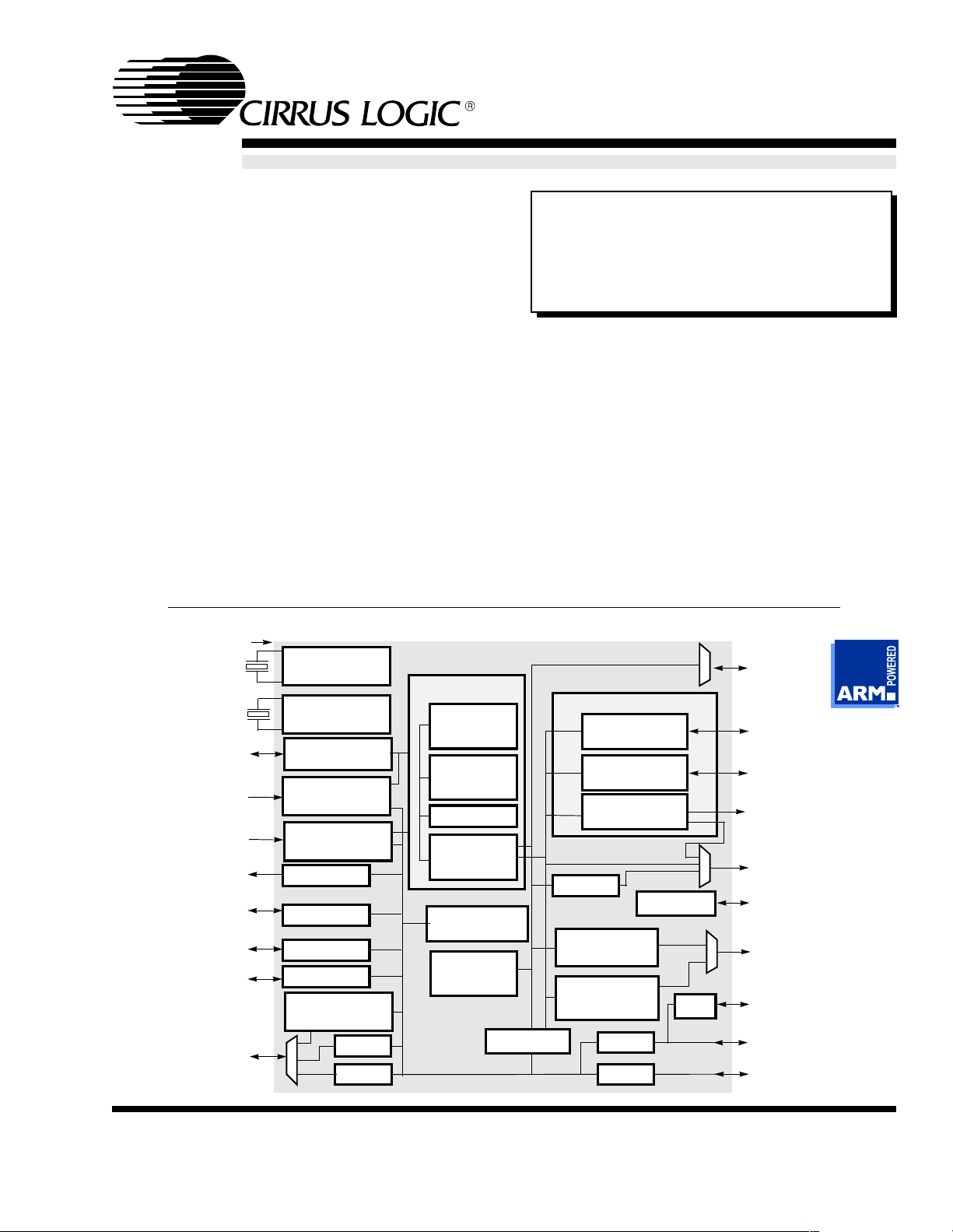
Functional Block Diagram
13-MHZ INPUT
3.6864 MHZ
32.768 KHZ
POR, RUN,
RESET, WAKEUP
BATOK, EXTPWR
PWRFL, BATCHG
EINT[1–3], FIQ,
MEDCHG
FLASHING LED DRIVE
PORTS A, B, D (8-BIT)
PORT E (3-BIT)
KEYBD DRIVERS (0–7)
BUZZER DRIVE
DC-TO-DC
ADCCLK, ADCIN,
ADCOUT, SMPCLK,
ADCCS
SSICLK, SSITXFR,
SSITXDA, SSIRXDA,
SSIRSFR
PLL
32.768-KHZ
OSCILLATOR
STATE CONTROL
POWER
MANAGEMENT
INTERRUPT
CONTROLLER
RTC
GPIO
PWM
SSI1 (ADC)
MULTIMEDIA
CODEC PORT
SSI2
CODEC
ARM720T
ARM7TDMI
CPU CORE
8-KBYTE
CACHE
WRITE
BUFFER
COUNTERS (2)
ON-CHIP
BOOT ROM
EPB BUS
MMU
TIMER
High-Performance Ultra-Low-
Power System-on-Chip with
LCD Controller
OVERVIEW
The EP7211 is designed for ultra-low-power applications such as organizers/PDAs, two-way pagers,
smart cellular phones, and industrial hand-held information appliances. The core-logic functionality of the
device is built around an ARM720T processor with 8
kbytes of four-way set-associative unified cache and
a write buffer. Incorporated into the ARM720T is an
enhanced memory management unit (MMU), which
allows for Microsoft Windows CE support.
The EP7211 also includes a 32-bit Y2K-compliant
Real Time Clock (RTC) and comparator.
APB BRIDGE
INTERNAL DATA BUS
MEMORY CONTROL BLOCK
CL-PS6700
INTFC.
EXPANSION
CONTROL
DRAM
CONTROLLER
INTERNAL ADDRESS BUS
LCD DMA
ICE-JTAG
LCD
CONTROLLER
ON-CHIP SRAM
37.5 KBYTES
UART1
UART2
IrDA
D0–D31
PB[0–1], CS[4–5]
EXPCLK, WORD,
CS[0–3], EXPRDY,
WRITE
MOE, MWE,
RAS[0–1], CAS[0–3]
A[0–27],
DRA[0–12]
TEST AND
DEVELOPMENT
LCD DRIVE
LED AND
PHOTODIODE
ASYNC
INTERFACE 1
ASYNC
INTERFACE 2
Cirrus Logic, Inc. Copyright © Cirrus Logic, Inc. 2001
P.O. Box 17847, Austin, Texas 78760 (All Rights Reserved)
(512) 445 7222 FAX: (512) 445 7851
http://www.cirrus.com
DS352PP3
JUL 2001
1
Page 2

High-Performance Ultra-Low-Power System-on-Chip with LCD Controller
FEATURES (cont.)
■ ARM720T processor
— ARM7TDMI CPU
— 8 kbytes of four-way set-associative cache
— MMU with 64-entry TLB (transition look aside buffer)
— Write buffer
— Windows
— Thumb
■ DRAM controller
— Supports both 16- and 32-bit-wide DRAMs
— EDO support (fast page mode support for 13 MHz and
18 MHz operation only)
■ ROM/SRAM/FLASH memory control
— Decodes 4, 5, or 6 separate memory segments of up to
256 Mbytes each
— Each segment can be configured as 8, 16, or 32 bits
wide and supports page-mode access
— Programmable access time for conventional
ROM/SRAM/Flash memory
■ 37.5 kbytes of on-chip SRAM for fast program
execution and/or as a frame buffer
■ On-chip ROM; for manufacturing boot-up support
■ Four synchronous serial interfaces
— ADC (SSI1) Interface: Master mode only; SPI1 and
Microwire1
— SSI2 Interface: Master/Slave mode; SPI/Microwire2
compatible (512 kbps operation)
— Audio Codec Interface (64 kbps operation)
— Multimedia Codec Port (Interfaces to Philips’ UCB1100
CE enabled
®
code support enabled
2
-compatible (128 kbps operation)
EP7211
and UCB1200 codecs) (9.216 Mbps operation)
■ 27 bits of general-purpose I/O
— Three 8-bit and one 3-bit GPIO port
— Supports scanning keyboard matrix
■ Two UARTs (16550 type)
— Supports bit rates up to 115.2 kbps
— Contains two 16-byte FIFOs for TX and RX
— UART1 supports modem control signals
■ SIR (up to 115.2 kbps) infrared encoder
— IrDA (Infrared Data Association) SIR protocol encoder
can be optionally switched into TX and RX signals of
UART1
■ PWM interface
— Provides two 96-kHz clock outputs with programmable
duty ratio (from 1-in-16 to 15-in-16) that can be used to
drive a DC-to-DC converter
■ Two timer counters
■ 208-pin LQFP or 256-ball PBGA packages
■ Evaluation kit available with BOM, schematics,
sample code, and design database
■ Support for up to two ultra-low-power CL-PS6700
PC Card controllers
■ Dedicated LED flasher pin from RTC
■ Full JTAG boundary scan and Embedded ICE
support
1
SPI is a registered trademark of Motorola.
2
Microwire is a registered trademark of National Semiconductor.
OVERVIEW (cont.)
Power Management
The EP7211 is designed for ultra-low-power operation. Its core operates at only 2.5 V, while its I/O has
an operating range of 2.5 V–3.3 V. The device has
three basic power states:
Operating — This state is the full performance
state. All the clocks and peripheral logic are
enabled.
Idle — This state is the same as the Operating
State, except the CPU clock is halted while waiting for an event such as a key press.
Standby — This state is equivalent to the computer
being switched off (no display), and the main
oscillator shut down. An event such as a key
press can wake up the processor.
2
Memory Interfaces
There are two main external memory interfaces.
The first one is the ROM/SRAM/Flash-style interface
that has programmable wait-state timings and
includes burst-mode capability, with six chip selects
each decoding 256-Mbyte sections of addressable
space. For maximum flexibility, each bank can be
specified to be 8, 16, or 32 bits wide. This allows the
use of 8-bit-wide boot ROM options to minimize overall system cost. The on-chip boot ROM can be used
in product manufacturing to serially download system
code into system Flash memory. To further minimize
system memory requirements and cost, the ARM
Thumb
instruction set is supported, providing for the
DS352PP3
JUL 2001
Page 3
EP7211
High-Performance Ultra-Low-Power System-on-Chip with LCD Controller
OVERVIEW (cont.)
use of high-speed 32-bit operations in 16-bit opcodes and yielding industry-leading code density.
The second is the programmable 16- or 32-bit-wide
DRAM interface that allows direct connection of up to
two banks of DRAM, each bank containing up to 256
Mbytes. To assure the lowest possible power consumption, the EP7211 supports self-refresh DRAMs,
which are placed in a low-power state by the device
when it enters the low-power Standby State. EDO
and Fast Page DRAM are supported.
A DMA address generator is also provided that
fetches video display frame buffer data for the LCD
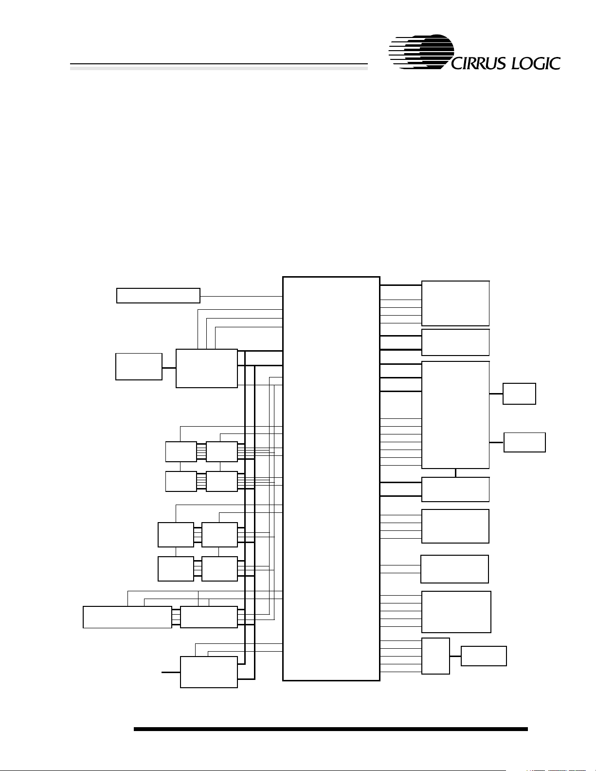
CRYSTAL
PC CARD
SOCKET
CL-PS6700
PC CARD
CONTROLLER
×16
DRAM
×16
DRAM
×16
FLASH
×16
DRAM
×16
DRAM
×16
ROM
MOSCIN
CS[4]
PB0
EXPCLK
D[31:0]
A[27:0]
MOE
WRITE
RAS[1]
RAS[0]
CAS[0]
CAS[1]
CAS[2]
CAS[3]
CS[0]
CS[1]
controller from main memory (typically DRAM). The
display frame buffer start address is programmable.
In addition, the built-in LCD controller can utilize
external or internal SRAM for memory, thus eliminating the need for DRAMs.
Serial Interfaces
The EP7211 includes two 16550-type UARTs for RS232 serial communications, both of which have two
16-byte FIFOs for receiving and transmitting data.
The UARTs support bit rates up to 115.2 kbps. An
IrDA SIR protocol encoder/decoder can be optionally
switched into the RX/TX signals to/from one of the
DD[3:0]
COL[7:0]
PA[7:0]
PB[7:0]
PD[7:0]
PE[2:0]
PWRFL
BATOK
EXTPWR
BATCHG
EP7211
WAKEUP
DRIVE[1:0]
FB[1:0]
SSICLK
SSITXFR
SSITXDA
SSIRXDA
CL1
CL2
FM
POR
RUN
LCD MODULE
M
KEYBOARD
POWER
SUPPLY UNIT
AND
COMPARATORS
DC-TO-DC
CONVERTERS
CODEC
DC
INPUT
BATTERY
EXTERNAL MEMORY-
MAPPED EXPANSION
ADDITIONAL I/O
DS352PP3
JUL 2001
×16
FLASH
×16
ROM
BUFFERS
BUFFERS
AND
LATCHES
LEDDRV
PHDIN
CS[n]
WORD
CS[2]
CS[3]
RXD1/2
TXD1/2
DSR
CTS
DCD
ADCCLK
ADCCS
ADCOUT
ADCIN
SMPCLK
TRANSCEIVERS
ADC
Figure 1-1. A EP7211–Based System
IR LED AND
PHOTODIODE
2× RS-232
DIGITIZER
3
Page 4

High-Performance Ultra-Low-Power System-on-Chip with LCD Controller
OVERVIEW (cont.)
UARTs to enable these signals to drive an infrared
communication interface directly.
Four synchronous serial interfaces (codec, SSI1,
SSI2, and MCP) are provided. Three of them (codec,
SSI2, and MCP) are multiplexed onto a single set of
interface pins. The full-duplex codec interface allows
direct connection of a standard audio codec chip to
the EP7211, allowing storage and playback of sound.
SSI2 supports both master and slave mode. SSI1
supports master mode only. Both SSI1 and SSI2 support two industry-standard protocols (SPI
Microwire
) for interfacing standard devices (e.g.,
Max148/9 or AD7811/12 ADC), and for allowing
peripheral expansion (e.g., a digitizer pen). A Multimedia Codec Port (MCP) can be used to communicate with a multi-functional codec device like the
Philips
UCB1100.
Packaging
and
EP7211
System Design
As shown in system block diagram, simply adding
desired memory and peripherals to the highly
integrated EP7211 completes a low-power system
solution. All necessary interface logic is integrated
on-chip.
Development Boards
Cirrus Logic offers an evaluation and development
environment for the EP7211 in the form of the
EDB7211-2 Development Kit.
The EDB7211-2 development kit is a complete development platform with access to the features and
capabilities of the EP7211. The kit provides the tools
required for developing and testing the design of a
highly integrated EP7211 system.
The EP7211 is available in a 208-pin LQFP package
and a 256-ball PBGA package.
Contacting Cirrus Logic Support
For a complete listing of Direct Sales, Distributor, and Sales Representative contacts, visit the Cirrus Logic web site at:
http://www.cirrus.com/corporate/contacts/
Preliminary product information describes products which are in production, but for which full characterization data is not yet available. Advance product information
describes products which are in development and subject to development changes. Cirrus Logic, Inc. has made best efforts to ensure that the information contained
in this document is accurate and reliable. However, the information is subject to change without notice and is provided “AS IS” without warranty of any kind (express
or implied). No responsibility is assumed by Cirrus Logic, Inc. for the use of this information, nor for infringements of patents or other rights of third parties. This document is the property of Cirrus Logic, Inc. and implies no license under patents, copyrights, trademarks, or trade secrets. No part of this publication may be copied,
reproduced, stored in a retrieval system, or transmitted, in any form or by any means (electronic, mechanical, photographic, or otherwise) without the prior written
consent of Cirrus Logic, Inc. Items from any Cirrus Logic website or disk may be printed for use by the user. However, no part of the printout or electronic files may
be copied, reproduced, stored in a retrieval system, or transmitted, in any form or by any means (electronic, mechanical, photographic, or otherwise) without the prior
written consent of Cirrus Logic, Inc.Furthermore, no part of this publication may be used as a basis for manufacture or sale of any items without the prior written consent
of Cirrus Logic, Inc. The names of products of Cirrus Logic, Inc. or other vendors and suppliers appearing in this document may be trademarks or service marks of
their respective owners which may be registered in some jurisdictions. A list of Cirrus Logic, Inc. trademarks and service marks can be found at http://www.cirrus.com.
4
DS352PP3
JUL 2001
Page 5

EP7211
High-Performance Ultra-Low-Power System-on-Chip with LCD Controller
TABLE OF CONTENTS
1. CONVENTIONS........................................................................................................................11
1.1 Acronyms and Abbreviations................................................................................................................... 11
1.2 Units of Measurement ............................................................................................................................. 12
1.3 General Conventions............................................................................................................................... 12
1.4 Pin Description Conventions ...................................................................................................................12
2. PIN INFORMATION..................................................................................................................13
2.1 Pin Diagrams...........................................................................................................................................13
2.2 Pin Descriptions ......................................................................................................................................14
2.2.1 External Signal Functions........................................................................................................... 15
2.3 256-Ball PBGA Ball Listing...................................................................................................................... 20
2.3.1 PBGA Ground Connections ....................................................................................................... 25
2.4 208-Pin LQFP Pin Listing ........................................................................................................................26
2.5 JTAG Pin Ordering for 208-Pin LQFP Package ......................................................................................31
3. FUNCTIONAL DESCRIPTION.................................................................................................34
3.1 Main Functional Blocks ........................................................................................................................... 35
3.2 CPU Core ................................................................................................................................................37
3.3 Interrupt Controller .................................................................................................................................. 37
3.3.1 Interrupt Latencies in Different States ........................................................................................39
3.3.1.1 Operating State ..........................................................................................................39
3.3.1.2 Idle State .................................................................................................................... 40
3.3.1.3 Standby State ............................................................................................................. 40
3.4 Memory and I/O Expansion Interface ...................................................................................................... 42
3.5 EP7211 Boot ROM ..................................................................................................................................43
3.6 CL-PS6700 PC Card Controller Interface ...............................................................................................44
3.7 DRAM Controller with EDO Support ....................................................................................................... 47
3.8 Serial Interfaces ...................................................................................................................................... 51
3.8.1 Codec Sound Interface............................................................................................................... 52
3.8.1.1 Codec Interrupt Timing...............................................................................................52
3.8.2 MCP Interface ............................................................................................................................ 53
3.8.2.1 MCP Operation ..........................................................................................................54
3.8.2.2 MCP Frame Format ...................................................................................................54
3.8.2.3 Audio and Telecom Sample Rates and Data Transfer ...............................................56
3.8.2.4 MCP FIFO Operation .................................................................................................58
3.8.2.5 MCP Codec Control Register Data Transfer .............................................................. 59
3.8.3 ADC Interface — Master Mode Only SSI1 (Synchronous Serial Interface) ...............................60
3.8.4 Master/Slave SSI2 (Synchronous Serial Interface 2) .................................................................61
3.8.4.1 Read Back of Residual Data ...................................................................................... 62
3.8.4.2 Support for Asymmetric Traffic ...................................................................................63
3.8.4.3 Continuous Data Transfer .......................................................................................... 63
3.8.4.4 Discontinuous Clock...................................................................................................63
3.8.4.5 Error Conditions .........................................................................................................64
3.8.4.6 Clock Polarity ............................................................................................................. 64
3.9 LCD Controller with Support for On-Chip Frame Buffer ..........................................................................64
3.10 Internal UARTs (Two) and SIR Encoder..................................................................................................67
3.11 Timer Counters........................................................................................................................................ 67
3.11.1 Free Running Mode....................................................................................................................68
DS352PP3
JUL 2001
5
Page 6

EP7211
High-Performance Ultra-Low-Power System-on-Chip with LCD Controller
3.11.2 Prescale Mode ........................................................................................................................... 68
3.12 Realtime Clock ........................................................................................................................................ 68
3.13 Dedicated LED Flasher ...........................................................................................................................68
3.14 Two PWM Interfaces ...............................................................................................................................69
3.15 State Control............................................................................................................................................ 69
3.16 Resets .....................................................................................................................................................72
3.17 Clocks...................................................................................................................................................... 73
3.17.1 On-Chip PLL............................................................................................................................... 73
3.17.2 External Clock Input (13 MHz) ................................................................................................... 74
3.18 Dynamic Clock Switching When in the PLL Clocking Mode....................................................................75
3.19 Endianness.............................................................................................................................................. 75
3.20 Maximum EP7211-Based System........................................................................................................... 77
3.21 Boundary Scan........................................................................................................................................ 78
3.22 In-Circuit Emulation .................................................................................................................................79
3.22.1 Introduction................................................................................................................................. 79
3.22.2 Functionality ...............................................................................................................................79
4. MEMORY MAP .........................................................................................................................80
5. REGISTER DESCRIPTIONS ...................................................................................................81
5.1 Internal Registers .................................................................................................................................... 81
5.1.1 PADR Port A Data Register........................................................................................................85
5.1.2 PBDR Port B Data Register ....................................................................................................... 85
5.1.3 PDDR Port D Data Register ....................................................................................................... 85
5.1.4 PADDR Port A Data Direction Register ...................................................................................... 85
5.1.5 PBDDR Port B Data Direction Register...................................................................................... 85
5.1.6 PDDDR Port D Data Direction Register ..................................................................................... 85
5.1.7 PEDR Port E Data Register ....................................................................................................... 86
5.1.8 PEDDR Port E Data Direction Register...................................................................................... 86
5.2 SYSTEM Control Registers .....................................................................................................................86
5.2.1 SYSCON1 The System Control Register 1 ................................................................................ 86
5.2.2 SYSCON2 System Control Register 2 ....................................................................................... 89
5.2.3 SYSCON3 System Control Register 3 ....................................................................................... 91
5.2.4 SYSFLG — The System Status Flags Register ......................................................................... 92
5.2.5 SYSFLG2 System Status Register 2..........................................................................................94
5.3 Interrupt Registers ...................................................................................................................................95
5.3.1 INTSR1 Interrupt Status Register 1............................................................................................95
5.3.2 INTMR1 Interrupt Mask Register 1.............................................................................................97
5.3.3 INTSR2 Interrupt Status Register 2............................................................................................97
5.3.4 INTMR2 Interrupt Mask Register 2.............................................................................................98
5.3.5 INTSR3 Interrupt Status Register 3............................................................................................98
5.3.6 INTMR3 Interrupt Mask Register 3.............................................................................................99
5.4 Memory Configuration Registers............................................................................................................. 99
5.4.1 MEMCFG1 Memory Configuration Register 1............................................................................99
5.4.2 MEMCFG2 Memory Configuration Register 2..........................................................................100
5.4.3 DRFPR DRAM Refresh Period Register .................................................................................. 102
5.5 Timer/Counter Registers .......................................................................................................................103
5.5.1 TC1D Timer Counter 1 Data Register ...................................................................................... 103
5.5.2 TC2D Timer Counter 2 Data Register ...................................................................................... 103
5.5.3 RTCDR Realtime Clock Data Register .....................................................................................103
5.5.4 RTCMR Realtime Clock Match Register .................................................................................. 103
6
DS352PP3
JUL 2001
Page 7

EP7211
High-Performance Ultra-Low-Power System-on-Chip with LCD Controller
5.6 LEDFLSH Register ................................................................................................................................104
5.7 PMPCON Pump Control Register ......................................................................................................... 105
5.8 CODR — The CODEC Interface Data Register .................................................................................... 106
5.9 UART Registers .................................................................................................................................... 106
5.9.1 UARTDR1–2 UART1–2 Data Registers ................................................................................... 106
5.9.2 UBRLCR1–2 UART1–2 Bit Rate and Line Control Registers................................................... 107
5.10 LCD Registers.......................................................................................................................................108
5.10.1 LCDCON — The LCD Control Register ................................................................................... 108
5.10.2 PALLSW Least Significant Word — LCD Palette Register ....................................................... 110
5.10.3 PALMSW Most Significant Word — LCD Palette Register ....................................................... 110
5.10.4 FBADDR LCD Frame Buffer Start Address .............................................................................. 111
5.11 SSI Register .......................................................................................................................................... 111
5.11.1 SYNCIO Synchronous Serial ADC Interface Data Register ..................................................... 111
5.12 STFCLR Clear all ‘Start Up Reason’ flags location ............................................................................... 113
5.13 ‘End Of Interrupt’ Locations................................................................................................................... 113
5.13.1 BLEOI Battery Low End of Interrupt ......................................................................................... 113
5.13.2 MCEOI Media Changed End of Interrupt ................................................................................. 113
5.13.3 TEOI Tick End of Interrupt Location ......................................................................................... 113
5.13.4 TC1EOI TC1 End of Interrupt Location .................................................................................... 113
5.13.5 TC2EOI TC2 End of Interrupt Location .................................................................................... 113
5.13.6 RTCEOI RTC Match End of Interrupt ....................................................................................... 113
5.13.7 UMSEOI UART1 Modem Status Changed End of Interrupt ..................................................... 114
5.13.8 COEOI Codec End of Interrupt Location .................................................................................. 114
5.13.9 KBDEOI Keyboard End of Interrupt Location ........................................................................... 114
5.13.10 SRXEOF End of Interrupt Location .......................................................................................... 114
5.14 State Control Registers ......................................................................................................................... 114
5.14.1 STDBY Enter the Standby State Location ................................................................................ 114
5.14.2 HALT Enter the Idle State Location .......................................................................................... 114
5.15 SS2 Registers ....................................................................................................................................... 115
5.15.1 SS2DR Synchronous Serial Interface 2 Data Register ............................................................ 115
5.15.2 SS2POP Synchronous Serial Interface 2 Pop Residual Byte .................................................. 115
5.16 MCP Register Definitions ...................................................................................................................... 115
5.16.1 MCP Control Register .............................................................................................................. 116
5.16.1.1 Audio Sample Rate Divisor (ASD) ........................................................................... 116
5.16.1.2 Telecom Sample Rate Divisor (TSD) ....................................................................... 117
5.16.1.3 Multimedia Communications Port Enable (MCE) ..................................................... 117
5.16.1.4 A/D Sampling Mode (ADM) ...................................................................................... 118
5.16.1.5 MCP Interrupt Generation ........................................................................................ 118
5.16.1.6 Telecom Transmit FIFO Interrupt Mask (TTM) ......................................................... 118
5.16.1.7 Telecom Receive FIFO Interrupt Mask (TRM) ......................................................... 118
5.16.1.8 Audio Transmit FIFO Interrupt Mask (ATM) ............................................................. 119
5.16.1.9 Audio Receive FIFO Interrupt Mask (ARM) ............................................................. 119
5.16.1.10 Loop Back Mode (LBM) ........................................................................................... 119
5.16.2 MCP Data Registers................................................................................................................. 121
5.16.2.1 MCP Data Register 0 ............................................................................................... 121
5.16.2.2 MCP Data Register 1 ............................................................................................... 123
5.16.2.3 MCP Data Register 2 ............................................................................................... 125
5.16.3 MCP Status Register ................................................................................................................ 127
DS352PP3
JUL 2001
7
Page 8

EP7211
High-Performance Ultra-Low-Power System-on-Chip with LCD Controller
5.16.3.1 Audio Transmit FIFO Service Request Flag (ATS) (read-only, maskable
interrupt)................................................................................................................... 127
5.16.3.2 Audio Receive FIFO Service Request Flag (ARS) (read-only, maskable interrupt) .127
5.16.3.3 Telecom Transmit FIFO Service Request Flag (TTS) (read-only,
maskable interrupt) ..................................................................................................127
5.16.3.4 Telecom Receive FIFO Service Request Flag (TRS) (read-only, maskable
interrupt)................................................................................................................... 128
5.16.3.5 Audio Transmit FIFO Underrun Status (ATU) (read/write, non-maskable interrupt). 128
5.16.3.6 Audio Receive FIFO Overrun Status (ARO) (read/write, non-maskable interrupt)...128
5.16.3.7 Telecom Transmit FIFO Underrun Status (TTU) (read/write, non-maskable
interrupt)................................................................................................................... 128
5.16.3.8 Telecom Receive FIFO Overrun Status (TRO) (read/write, non-maskable
interrupt)................................................................................................................... 128
5.16.3.9 Audio Transmit FIFO Not Full Flag (ANF) (read-only, non-interruptible) .................. 129
5.16.3.10 Audio Receive FIFO Not Empty Flag (ANE) (read-only, non-interruptible) .............. 129
5.16.3.11 Telecom Transmit FIFO Not Full Flag (TNF) (read-only, non-interruptible) ..............129
5.16.3.12 Telecom Receive FIFO Not Empty Flag (TNE) (read-only, non-interruptible) .......... 129
5.16.3.13 Codec Write Completed Flag (CWC) (read-only, non-interruptible) ......................... 129
5.16.3.14 Codec Read Completed Flag (CRC) (read-only, non-interruptible)..........................129
5.16.3.15 Audio Codec Enabled Flag (ACE) (read-only, non-interruptible).............................. 130
5.16.3.16 Telecom Codec Enabled Flag (TCE) (read-only, non-interruptible).......................... 130
6. ELECTRICAL SPECIFICATIONS......................................................................................... 133
6.1 Absolute Maximum Ratings................................................................................................................... 133
6.2 Recommended Operating Conditions ................................................................................................... 133
6.3 DC Characteristics ................................................................................................................................ 133
6.4 AC Characteristics................................................................................................................................. 135
6.5 I/O Buffer Characteristics ......................................................................................................................150
7. TEST MODES ........................................................................................................................ 151
7.1 Oscillator and PLL Bypass Mode ..........................................................................................................151
7.2 Oscillator and PLL Test Mode ...............................................................................................................151
7.3 Debug/ICE Test Mode ..........................................................................................................................152
7.4 Hi-Z (System) Test Mode...................................................................................................................... 152
7.5 Software Selectable Test Functionality................................................................................................. 152
8. PACKAGE SPECIFICATIONS.............................................................................................. 154
8.1 EP7211 256-Ball PBGA (17 × 17 × 1.53-mm Body) Dimensions .......................................................... 154
8.2 208-Pin LQFP Package Outline Drawing .............................................................................................155
9. ORDERING INFORMATION ................................................................................................. 156
10. APPENDIX A: BOOT CODE................................................................................................. 157
11. INDEX..................................................................................................................................... 162
8
DS352PP3
JUL 2001
Page 9

EP7211
High-Performance Ultra-Low-Power System-on-Chip with LCD Controller
LIST OF TABLES
Table 2-1. SSI/Codec/MCP Pin Multiplexing.................................................................................................... 18
Table 2-2. 256-Ball PBGA Ball Listing ............................................................................................................ 20
Table 2-3. PBGA Balls to Connect to Ground (V
Table 2-4. 208-Pin LQFP Numeric Pin Listing ................................................................................................. 24
Table 2-5. JTAG Pin Ordering for 208-Pin LQFP Package ............................................................................. 28
Table 3-1. Interrupt Allocation in First Interrupt Register ................................................................................. 35
Table 3-2. Interrupt Allocation in Second Interrupt Register ............................................................................ 36
Table 3-3. Interrupt Allocation in Third Interrupt Register ................................................................................ 36
Table 3-4. External Interrupt Source Latencies................................................................................................ 38
Table 3-5. Boot Options ................................................................................................................................... 40
Table 3-6. Chip Select Address Ranges After Boot From On-Chip Boot ROM ............................................... 40
Table 3-7. CL-PS6700 Memory Map ............................................................................................................... 41
Table 3-8. Space Field Decoding..................................................................................................................... 42
Table 3-9. Physical to DRAM Address Mapping .............................................................................................. 45
Table 3-10. DRAM Address Mapping When Connected to an External 32-Bit DRAM Memory System ........... 46
Table 3-11. DRAM Address Mapping for a 16-Bit-Wide DRAM Memory System .............................................. 47
Table 3-12. Serial Interface Options .................................................................................................................. 48
Table 3-13. Serial-Pin Assignments ................................................................................................................... 48
Table 3-14. ADC Interface Operation Frequencies............................................................................................ 57
Table 3-15. Peripheral Status in Different Power Management States.............................................................. 67
Table 3-16. Effect of Endianness on Read Operations...................................................................................... 73
Table 3-17. Effect of Endianness on Write Operations ...................................................................................... 73
Table 3-18. Instructions Supported in JTAG Mode ............................................................................................ 75
Table 4-1. EP7211 Memory Map ..................................................................................................................... 77
Table 5-1. CL-PS7111-Compatible................................................................................................................... 79
Table 5-2. Internal I/O Memory Locations (EP7211 Only) ............................................................................... 81
Table 5-3. Port Byte Addresses in Big Endian Mode ....................................................................................... 81
Table 5-4. Values of the Bus Width Field ......................................................................................................... 97
Table 5-5. Values of the Wait State Field at 13 MHz and 18 MHz ...................................................................98
Table 5-6. Values of the Wait State Field at 36 MHz........................................................................................ 98
Table 5-7. LED Flash Rates........................................................................................................................... 101
Table 5-8. LED Duty Ratio ............................................................................................................................. 101
Table 5-9. Sense of PWM control lines.......................................................................................................... 102
Table 5-10. UART Bit Rates Running from the PLL Clock............................................................................... 104
Table 5-11. UART Bit Rates Running from an External 13.0 MHz Clock ........................................................ 104
Table 5-12. Grey Scale Value to Color Mapping .............................................................................................. 107
Table 5-13. MCP Control Register ................................................................................................................... 117
Table 5-14. MCP Data Register 0 .................................................................................................................... 120
Table 5-15. MCP Data Register 1 .................................................................................................................... 121
Table 5-16. MCP Data Register 2 .................................................................................................................... 123
Table 5-17. MCP Control, Data and Status Register Locations ....................................................................... 128
Table 6-1. DC Characteristics ........................................................................................................................ 130
Table 6-2. AC Timing Characteristics ............................................................................................................ 132
Table 6-3. Timing Characteristics .................................................................................................................. 133
Table 6-4. I/O Buffer Output Characteristics .................................................................................................. 147
Table 7-1. EP7211 Hardware Test Modes ..................................................................................................... 148
Table 7-2. Oscillator and PLL Test Mode Signals .......................................................................................... 149
Table 7-3. Software Selectable Test Functionality ......................................................................................... 150
) ........................................................................................ 23
SS
DS352PP3
JUL 2001
9
Page 10

EP7211
High-Performance Ultra-Low-Power System-on-Chip with LCD Controller
LIST OF FIGURES
Figure 1-1. A EP7211–Based System................................................................................................................... 3
Figure 2-1. 208-Pin LQFP (Low Profile Quad Flat Pack) Pin Diagram ............................................................... 13
Figure 2-2. 256-Ball Plastic Ball Grid Array Diagram .......................................................................................... 14
Figure 3-1. EP7211 Block Diagram ..................................................................................................................... 37
Figure 3-2. Codec Interrupt Timing ..................................................................................................................... 52
Figure 3-3. Data Format of MCP Subframe 0 ..................................................................................................... 55
Figure 3-4. MCP Packet Organization ................................................................................................................ 55
Figure 3-5. Audio Codec Enable Timing .............................................................................................................57
Figure 3-6. Format for the Audio and Telecom FIFOs......................................................................................... 59
Figure 3-7. SSI2 Port Directions in Slave and Master Mode............................................................................... 61
Figure 3-8. Residual Byte Reading ..................................................................................................................... 63
Figure 3-9. Video Buffer Mapping ....................................................................................................................... 66
Figure 3-10. State Diagram ................................................................................................................................... 72
Figure 3-11. CLKEN Timing Entering the Standby State.......................................................................................74
Figure 3-12. CLKEN Timing Leaving the Standby State ...................................................................................... 75
Figure 3-13. A Maximum EP7211 Based System ................................................................................................. 77
Figure 5-1. MCP Data Register 0: MCDR0 ....................................................................................................... 122
Figure 5-2. MCP Data Register 1: MCDR1 ....................................................................................................... 124
Figure 5-3. MCP Data Register 2: MCDR2 ....................................................................................................... 126
Figure 5-4. MCP Status Register: MCSR ......................................................................................................... 131
Figure 6-1. Expansion and ROM Timing ...........................................................................................................137
Figure 6-2. Expansion and ROM Sequential Read Timings..............................................................................138
Figure 6-3. Expansion and ROM Write Timings................................................................................................139
Figure 6-4. DRAM Read Cycles at 13 MHz and 18.432 MHz ........................................................................... 140
Figure 6-5. DRAM Read Cycles at 36 MHz ...................................................................................................... 141
Figure 6-6. DRAM Write Cycles at 13 MHz and 18 MHz .................................................................................. 142
Figure 6-7. DRAM Write Cycles at 36 MHz....................................................................................................... 143
Figure 6-8. Video Quad Word Read from DRAM at 13 MHz and 18 MHz ........................................................ 144
Figure 6-9. Quad Word Read from DRAM at 36 MHz .......................................................................................145
Figure 6-10. DRAM CAS Before RAS Refresh Cycle at 13 MHz and 18 MHz.................................................... 146
Figure 6-11. DRAM CAS Before RAS Refresh Cycle at 36 MHz ........................................................................ 147
Figure 6-12. LCD Controller Timings................................................................................................................... 148
Figure 6-13. SSI Interface for AD7811/2 ............................................................................................................. 148
Figure 6-14. SSI Timing Interface for MAX148/9 ................................................................................................149
Figure 6-15. SSI2 Interface Timings.................................................................................................................... 149
10
DS352PP3
JUL 2001
Page 11
EP7211
High-Performance Ultra-Low-Power System-on-Chip with LCD Controller
1. CONVENTIONS
This section presents acronyms, abbreviations, units of measurement, and conventions used in this
data book.
1.1 Acronyms and Abbreviations
The following table lists abbreviations and acronyms used in this data book.
Acronym/
Abbreviation
AC alternating current
A/D analog-to-digital
ADC analong-to-digital converter
codec coder/decoder
CMOS complementary metal oxide
semiconductor
CPU central processing unit
D/A digital-to-analog
DC direct current
DMA direct-memory access
DRAM dynamic random access memory
EPB embedded peripheral bus
FCS frame check sequence
FIFO first in/first out
GPIO general purpose I/O
ICT in circuit test
IR infrared
IrDA Infrared Data Association
JTAG Joint Test Action Group
LCD liquid crystal display
LED light-emitting diode
LSB least significant bit
Definition
Acronym/
Abbreviation
MIPS millions of instructions per second
LQFP low profile quad flat pack
MMU memory management unit
MSB most significant bit
PBGA plastic ball grid array
PCB printed circuit board
PDA personal digital assistant
PIA peripheral interface adapter
PLL phase locked loop
PSU power supply unit
p/u pull-up resistor
RAM random access memory
RISC reduced instruction set computer
ROM read-only memory
RTC realtime clock
SIR slow (9600–115.2 kbps) infrared
SRAM static random access memory
SSI synchronous serial interface
TAP test access port
TLB translation look aside buffer
UART universal asynchronous receiver
transmitter
Definition
DS352PP3
JUL 2001
Conventions
11
Page 12
1.2 Units of Measurement
\
Symbol Unit of Measure
EP7211
High-Performance Ultra-Low-Power System-on-Chip with LCD Controller
Symbol Unit of Measure
°C
Hz hertz (cycle per second)
kbits/s kilobits per second
kbyte kilobyte (1,024 bytes)
kHz kilohertz
kΩ kilohm
Mbps megabits (1,048,576 bits) per second
Mbyte megabyte (1,048,576 bytes)
MHz megahertz (1,000 kilohertz)
µA microampere
degree Celsius
µF microfarad
µWmicrowatt
µs microsecond (1,000 nanoseconds)
mA milliampere
mW milliwatt
ms millisecond (1,000 microseconds)
ns nanosecond
Vvolt
Wwatt
1.3 General Conventions
Hexadecimal numbers are presented with all letters in uppercase and a lowercase h appended. For
example, 14h and 03CAh are hexadecimal numbers. Binary numbers are enclosed in single quotation
marks when in text (for example, ‘11’ designates a binary number). Numbers not indicated by an h
or quotation marks are decimal.
Registers are referred to by acronym, as listed in the tables on the previous page, with bits listed in
brackets MSB-to-LSB separated by a colon (:) (for example, CODR[7:0]), or LSB-to-MSB
separated by a hyphen (for example, CODR[0–2]).
The use of ‘tbd’ indicates values that are ‘to be determined’, ‘n/a’ designates ‘not available’, and
‘n/c’ indicates a pin that is a ‘no connect’.
1.4 Pin Description Conventions
Abbreviations used for signal directions in Section 2 are listed in the following table:
Abbreviation Direction
I Input
OOutput
I/O Input or Output
12
Conventions
DS352PP3
JUL 2001
Page 13
EP7211
High-Performance Ultra-Low-Power System-on-Chip with LCD Controller
2. PIN INFORMATION
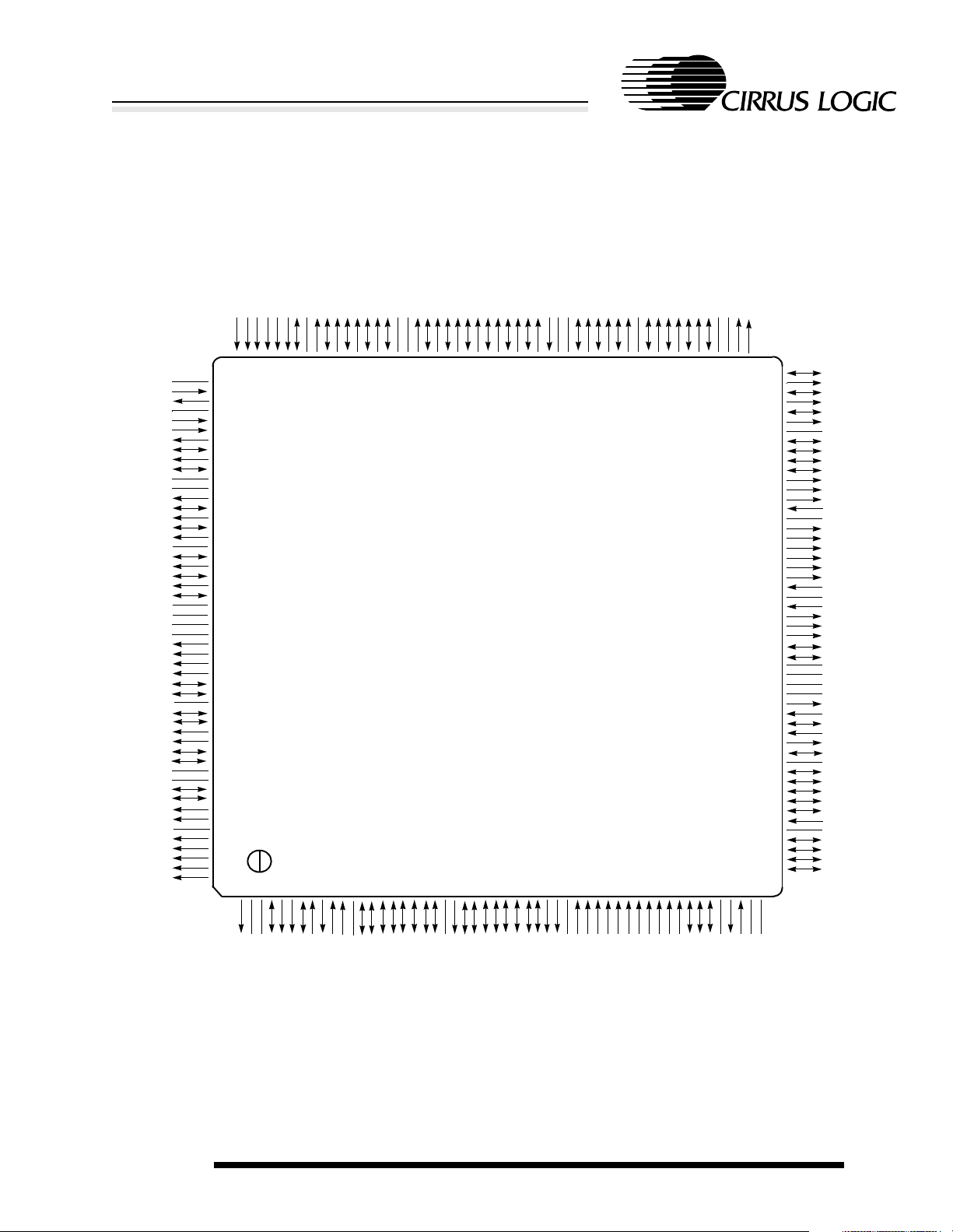
2.1 Pin Diagrams
NMEDCHG/NBROM
NEXTPWR
NURESET
NPOR
D[7]
A[7]
D[8]
A[8]
D[9]
D[10]
A[10]
VSSIO
VDDIO
A[11]
D[12]
A[12]
D[13]
A[13]
D[14]
NBATCHG
VSSIO
BATOK
D[11]
A[9]
A[14]
D[17]
D[15]
A[15]/DRA[12]
A[17]/DRA[10]
NTRST
A[16]/DRA[11]
VSSIO
D[16]
VDDIO
D[18]
A[18]/DRA[9]
D[19]
A[19]/DRA[8]
D[20]
VSSIO
A[21]/DRA[6]
D[22]
D[23]
A[23]/DRA[4]
D[24]
VSSIO
VDDIO
A[24]/DRA[3]
A[22]/DRA[5]
D[21]
A[20]/DRA[7]
HALFWORD
VDDOSC
MOSCIN
MOSCOUT
VSSOSC
WAKE UP
NPWRFL
A[6]
D[6]
A[5]
D[5]
VDDIO
VSSIO
A[4]
D[4]
A[3]
D[3]
A[2]
VSSIO
D[2]
A[1]
D[1]
A[0]
D[0]
VSSCORE
VDDCORE
VSSIO
VDDIO
CL[2]
CL[1]
FRM
DD[3]
DD[2]
VSSIO
DD[1]
DD[0]
NRAS[1]
NRAS[0]
NCAS[3]
NCAS[2]
VDDIO
VSSIO
NCAS[1]
NCAS[0]
NMWE
NMOE
VSSIO
NCS[0]
NCS[1]
NCS[2]
NCS[3]
NCS[4]
130
131
132
156
155
154
153
152
151
150
149
148
147
146
145
144
143
140
139
141
157
158
159
160
161
162
163
164
165
166
167
168
169
170
171
172
173
174
175
176
177
178
179
180
181
182
183
184
185
186
M
187
188
189
190
191
192
193
194
195
196
197
198
199
200
201
202
203
204
205
206
207
208
2345678910111213141516171819202122232425262728293031323334353637383940414243444546474849515052
1
142
134
138
137
136
135
133
EP7211
208-Pin LQFP
(Top View)
123
111
105
104
103
102
101
100
99
98
97
96
95
94
93
92
91
90
89
88
87
86
85
84
83
82
81
80
79
78
77
76
75
74
73
72
71
70
69
68
67
66
65
64
63
62
61
60
59
58
57
56
55
54
53
106
107
108
109
110
112
113
114
115
116
117
118
119
120
121
122
124
125
126
127
128
129
D[25]
A[25]/DRA[2]
D[26]
A[26]/DRA[1]
D[27]
A[27]/DRA[0]
VSSIO
D[28]
D[29]
D[30]
D[31]
BUZ
COL[0]
COL[1]
TCLK
VDDIO
COL[2]
COL[3]
COL[4]
COL[5]
COL[6]
COL[7]
FB[0]
VSSIO
FB[1]
SMPCLK
ADCOUT
ADCCLK
DRIVE[0]
DRIVE[1]
VDDIO
VSSIO
VDDCORE
VSSCORE
NADCCS
ADCIN
SSIRXFR
SSIRXDA
SSITXDA
SSITXFR
VSSIO
SSICLK
PD[0]/LEDFLSH
PD[1]
PD[2]
PD[3]
TMS
VDDIO
PD[4]
PD[5]
PD[6]
PD[7]
DS352PP3
JUL 2001
NCS[5]
VSSIO
VDDIO
TDI
PB[7]
PB[6]
PB[5]
PB[4]
TXD[2]
WORD
WRITE
EXPCLK
VSSIO
RXD[2]
EXPRDY
PB[3]
RUN/CLKEN
TDO
PB[2]
PB[1]/PRDY[2]
PA[6]
PA[5]
PA[4]
PA[3]
PA[2]
PA[1]
VDDIO
PA[7]
PA[0]
PB[0]/PRDY[1]
TXD[1]
LEDDRV
CTS
DSR
DCD
VSSIO
PHDIN
RXD[1]
EINT[3]
NEINT[2]
NEINT[1]
NTEST[1]
NEXTFIQ
NTEST[0]
PE[2]/CLKSEL
PE[1]BOOTSEL[1]
PE[0]BOOTSEL[0]
N/C
RTCIN
VDDRTC
VSSRTC
RTCOUT
Figure 2-1. 208-Pin LQFP (Low Profile Quad Flat Pack) Pin Diagram
Pin Information
13
Page 14
High-Performance Ultra-Low-Power System-on-Chip with LCD Controller
16 15 14 13 12 11 10 9 8 7 6 5 4 3 2 1
EP7211
A
B
C
D
E
F
G
H
256-Ball PBGA
(Bottom View)
(Call Factory for Availability)
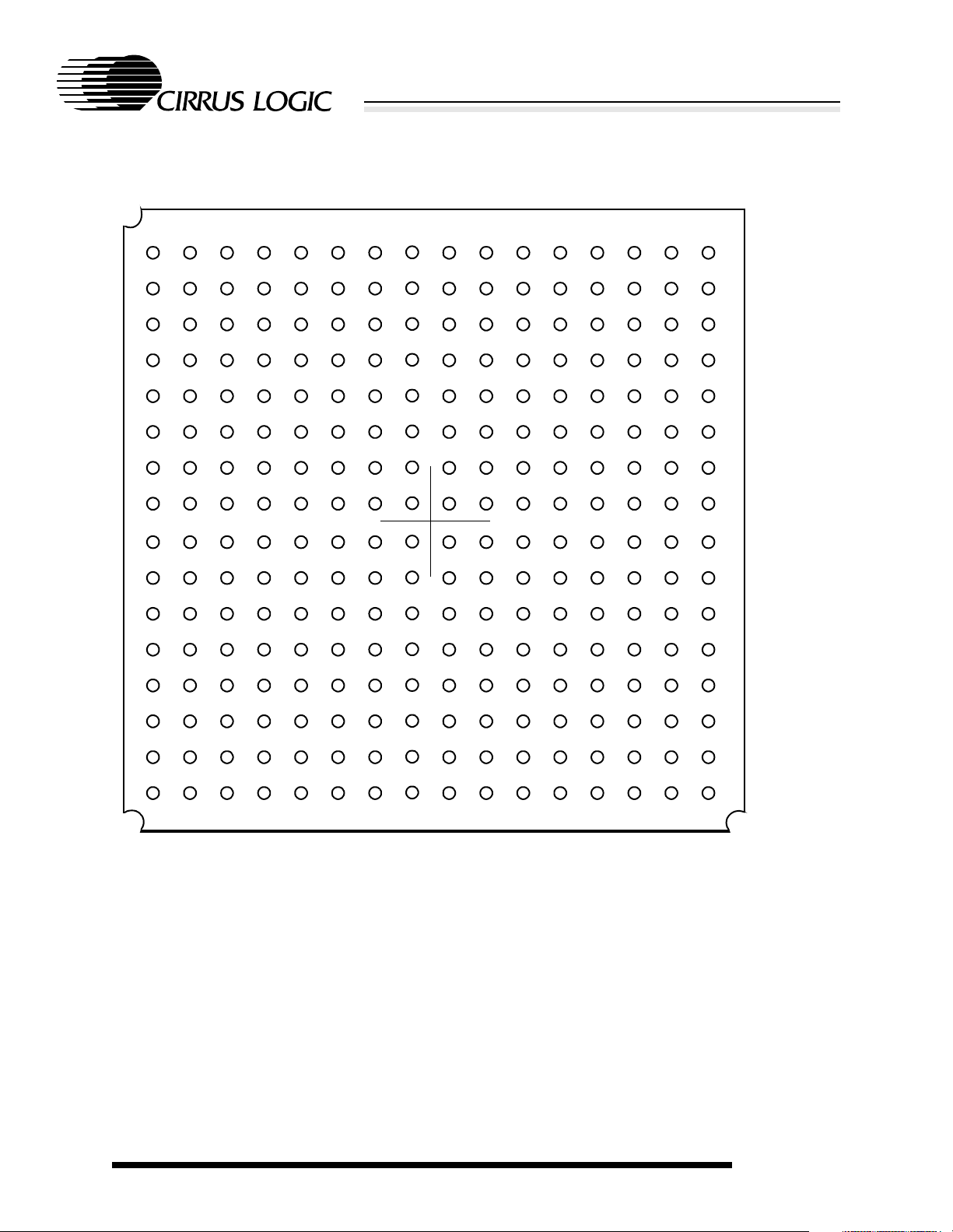
Figure 2-2. 256-Ball Plastic Ball Grid Array Diagram
J
K
L
M
N
P
R
T
2.2 Pin Descriptions
This table describes the function of all the external signals to the EP7211. Note that all output signals
are tri-stateable to enable the Hi-Z test modes to be supported.
14
Pin Information
DS352PP3
JUL 2001
Page 15

EP7211
High-Performance Ultra-Low-Power System-on-Chip with LCD Controller
2.2.1 External Signal Functions
Function
Data bus D[0–31] I/O 32-bit system data bus for DRAM, ROM/SRAM/Flash, and memory mapped
Address bus
Signal
Name
A[0–14] O Least significant 15 bits of system byte address during ROM/SRAM/Flash and
A[15]/
DRA[12]–
A[27]/DRA[0]
NRAS[0–1] O DRAM RAS outputs to DRAM banks 0 to 1
NCAS[0–3] I/O DRAM CAS outputs for bytes 0 to 3 within 32-bit word
NMOE O DRAM, ROM/SRAM/Flash, and expansion output enable
NMWE O DRAM, ROM/SRAM/Flash, and expansion write enable
Signal Description
I/O expansion
expansion cycles
O 13-bit multiplexed DRAM word address during DRAM cycles or address bits
16 to 27 of system byte address during ROM/SRAM/Flash and expansion
cycles
– Whenever the EP7211 is in the Standby State, the external address and
data buses are driven low. The RUN signal is used internally to force these
buses to be driven low. This is done to prevent peripherals that are powerdown from draining current. Also, the internal peripheral’s signals get set to
their Reset State
– For additional power saving, the multiplexed DRAM address lines are output
on the high order ROM address lines where the lightest loading is expected.
.
Memory and
Expansion
Interface
NCS[0–3] O Expansion channel I/O strobes; active low SRAM-like chip selects for expan-
sion
NCS[4–5] O Expansion channel I/O strobes; active low CS for expansion or for
CL-PS6700 select
EXPRDY I/O Expansion channel ready; external expansion devices drive this low to extend
the bus cycle
WRITE O Transfer direction, low during reads, high during writes from the
EP7211
WORD O Word access enable; driven high during word-wide cycles, low during byte-
wide cycles
HALFWORD O Half-Word access flag; driven high to denote upper half-word accesses
EXPCLK I/O Expansion clock rate is the same as the CPU clock for 13 MHz and 18 MHz. It
runs at 36.864 MHz for 36,49 and 74 MHz modes; in 13 MHz mode this pin is
used as the clock input
DS352PP3
JUL 2001
Pin Information
15
Page 16

EP7211
High-Performance Ultra-Low-Power System-on-Chip with LCD Controller
Function
Interrupts
Power
Management
Signal
Name
NMEDCHG/
BROM
NEXTFIQ I External active low fast interrupt request input
EINT3 I External active high interrupt request input
NEINT[1–2] I Two general purpose, active low interrupt inputs
NPWRFL I Power fail input; active low deglitched input to force system into the Standby
BATOK I Main battery OK input; falling edge generates a FIQ, a low level in the Standby
NEXTPWR I External power sense; must be driven low if the system is powered by an
NBATCHG I New battery sense; driven low if battery voltage falls below the "no-battery"
NPOR I Power-on reset input; active low input completely resets the entire system;
Signal Description
I Media changed input; active low, deglitched — it is used as a general purpose
FIQ interrupt during normal operation. It is also used on power up to configure
the processor to either boot from the internal Boot ROM, or from external
memory. When low, the chip will boot from the internal Boot ROM.
State
State inhibits system start up; deglitched input
external source
threshold; it is a deglitched input
must be held active for at least two clock cycles to be detected cleanly
State Control
MCP, Codec or
SSI2
Interface
(See Note)
RUN/CLKEN This pin is programmed to either output the RUN signal or the CLKEN signal.
The CLKENSL bit is used to configure this pin. When RUN is selected, the pin
will be high when the system is active or idle, low while in the Standby State.
When CLKEN is selected, the pin will only be driven low when in the Standby
State.
WAKEUP I Wake up deglitched input signal; rising edge forces system into the Operating
State; active after a power-on reset
NURESET I User reset input; active low deglitched input from user reset button.
This pin is also latched upon the rising edge of NPOR and read along with the
input pins NTEST[0–1] to force the device into special test modes.
SSICLK I/O MCP/Codec/SSI2 clock signal
SSITXFR I/O MCP/Codec/SSI2 serial data output frame/synchronization pulse output
SSITXDA O MCP/Codec/SSI2 serial data output
SSIRXDA I MCP/Codec/SSI2 serial data input
SSIRXFR I/O SSI2 serial data input frame/synchronization pulse
16
Pin Information
DS352PP3
JUL 2001
Page 17

EP7211
High-Performance Ultra-Low-Power System-on-Chip with LCD Controller
Function
ADC
Interface
(SSI1)
IrDA and
RS232
Interfaces
Signal
Name
ADCCLK O Serial clock output
NADCCS O Chip select for ADC interface
ADCOUT O Serial data output
ADCIN I Serial data input
SMPCLK O Sample clock output
LEDDRV O Infrared LED drive output (UART1)
PHDIN I Photo diode input (UART1)
TXD[1–2] O RS232 UART1 and 2 TX outputs
RXD[1–2] I RS232 UART1 and 2 RX inputs
DSR I RS232 DSR input
DCD I RS232 DCD input
CTS I RS232 CTS input
DD[0–3] I/O LCD serial display data; pins can be used on power up to read the ID of some
Signal Description
LCD modules
LCD
Keyboard &
Buzzer drive
LED Flasher
General
Purpose I/O
CL1 O LCD line clock
CL2 O LCD pixel clock
FRM O LCD frame synchronization pulse output
M O LCD AC bias drive
COL[0–7] O Keyboard column drives
BUZ O Buzzer drive output
PD[0]/
LEDFLSH
PA[0–7] I/O Port A I/O (Bit 6 for boot clock option, Bit 7 for CL-PS6700 PRDY input); also
PB[0]/PRDY1 I/O Port B I/O. All eight Port B bits can be used as GPIOs.
PB[1]/PRDY2
PB[2–7]
PD[0–7] I/O Port D I/O
O LED flasher driver — multiplexed with Port D Bit 0. This pin can provide up to
4 mA of drive current.
used as keyboard row inputs
When the PC CARD1 or 2 control bits in the SYSCON2 register are deasserted, PB[0] and PB[1] are available for GPIO. When asserted, these port
bits are used as the PRDY signals for connected
CL-PS6700 PC Card Host Adapter devices.
DS352PP3
JUL 2001
Pin Information
17
Page 18

EP7211
High-Performance Ultra-Low-Power System-on-Chip with LCD Controller
Function
PWM
Drives
Boundary
Scan
Signal
Name
PE[0]/
BOOTSEL0
PE[1]/
BOOTSEL1
PE[2]/
CLKSEL
DRIVE[0–1] I/O PWM drive outputs. These pins are inputs on power up to determine what
FB[0–1] I PWM feedback inputs
TDI I JTAG data in
TDO O JTAG data out
TMS I JTAG mode select
TCLK I JTAG clock
Signal Description
I/O Port E I/O (3 bits only). Can be used as general purpose I/O during normal
operation.
I/O During power-on reset, PE[0] and PE[1] are inputs and are latched by the ris-
ing edge of NPOR to select the memory width that the
EP7211 will use to read from the boot code storage device (e.g., external 8-bitwide Flash bank).
I/O During power-on reset, PE[2] is latched by the rising edge of NPOR to select
the clock mode of operation (i.e., either the PLL or external
13 MHz clock mode).
polarity the output of the PWM should be when active. Otherwise, these pins
are always an output.
TNRST I JTAG async reset
Test NTEST[0–1] I Test mode select inputs. These pins are used in conjunction with the power-on
latched state of NURESET.
MOSCIN
MOSCOUT
Oscillators
RTCIN
RTCOUT
I
O
I
O
Main 3.6864 MHz oscillator for 18.432MHz–73.728 MHz PLL
Realtime clock 32.768 kHz oscillator
NOTE: See table below for pin assignment and direction following pin multiplexing.
.
Table 2-1. SSI/Codec/MCP Pin Multiplexing
SSI2 Codec MCP Direction Strength
SSICCLK PCMCLK SIBCLK I/O 1
SSITXFR PCMSYNC SIBSYNC I/O 1
SSITXDA PCMOUT SIBDOUT Output 1
SSIRXDA PCMIN SIBDIN Input
SSIRXFR p/u* p/u* I/O 1
18
* p/u = use an ~10 k pull-up
Pin Information
DS352PP3
JUL 2001
Page 19

EP7211
High-Performance Ultra-Low-Power System-on-Chip with LCD Controller
The selection between SSI2 and the codec is controlled by the state of the SERSEL bit in SYSCON2
(Section 5.2.2 SYSCON2 System Control Register 2). The choice between the SSI2, codec, and
the MCP is controlled by the MCPSEL bit in SYSCON3 (Section 5.2.3 SYSCON3 System Control
Register 3).
NOTE: All deglitched inputs are via the 16.384 kHz clock. Therefore, the input signal must be active for at
least ~61 µs to be detected cleanly.
The following output pins are implemented as bi-directional pins to enable the output side of the pad
to be monitored and hence provide more accurate control of timing or duration:
RUN The RUN pin is looped back in to skew the address and data bus from each other.
NCAS[3:0] The NCAS pins are looped back into the EP7211 to be used as the actual clock
source for the data to be latched internally.
Drive 0 and 1 Drive 0 and 1 are looped back in on power up to determine what polarity the output
of the PWM should be when active.
DD[3:0] DD[3:0] are looped back in on power up to enable the reading of the ID of some
LCD modules.
DS352PP3
JUL 2001
Pin Information
19
Page 20
EP7211
High-Performance Ultra-Low-Power System-on-Chip with LCD Controller
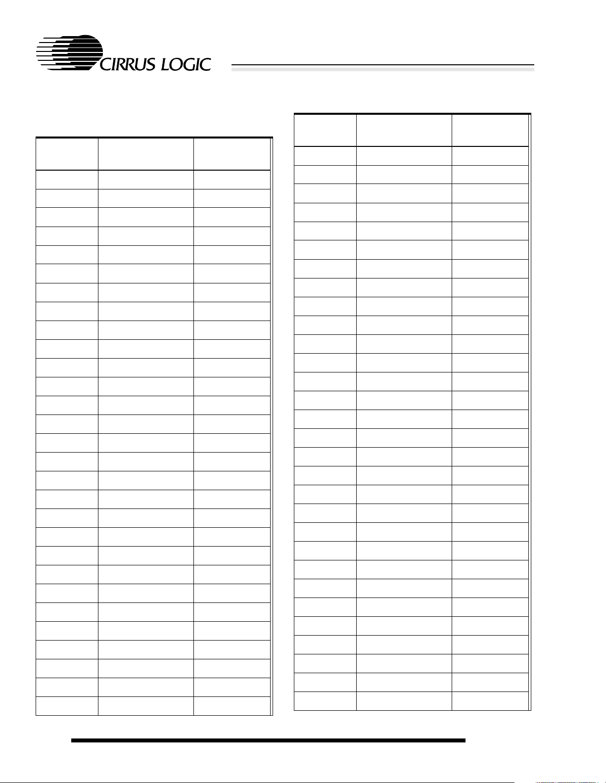
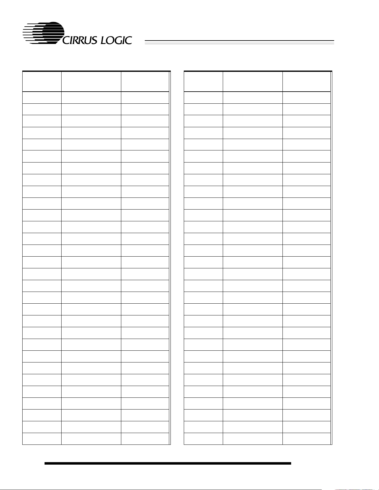
2.3 256-Ball PBGA Ball Listing
Table 2-2. 256-Ball PBGA Ball Listing
Ball
Location
A1 VDDIO Pad power
A2 NCS[4] O
A3 NCS[1] O
A4 NCAS[0] O
A5 NCAS[3] O
A6 DD[1] O
A7 M O
A8 VDDIO Pad power
A9 D[0] I/O
A10 D[2] I/O
A11 A[3] O
A12 VDDIO Pad power
A13 A[6] O
A14 MOSCOUT O
A15 VDDOSC Oscillator power
A16 VSSIO Pad ground
B1 NCS[5] O
B2 VDDIO Pad power
B3 NCS[3] O
B4 NMOE O
B5 VDDIO Pad power
B6 NRAS[1] O
B7 DD[2] O
B8 CL[1] O
B9 VDDCORE Core power
B10 D[1] I/O
B11 A[2] O
B12 A[4] O
B13 A[5] O
Name Type
Table 2-2. (cont.)256-Ball PBGA Ball Listing
Ball
Location
B14 WAKEUP I
B15 VSSIO Pad ground
B16 NURESET I
C1 VDDIO Pad power
C2 EXPCLK I
C3 VSSIO Pad ground
C4 VDDIO Pad power
C5 VSSIO Pad ground
C6 VSSIO Pad ground
C7 VSSIO Pad ground
C8 VDDIO Pad power
C9 VSSIO Pad ground
C10 VSSIO Pad ground
C11 VSSIO Pad ground
C12 VDDIO Pad power
C13 VSSIO Pad ground
C14 VSSIO Pad ground
C15 NPOR I
C16 NEXTPWR I
D1 WRITE O
D2 EXPRDY I
D3 VSSIO Pad ground
D4 VDDIO Pad power
D5 NCS[2] O
D6 NMWE O
D7 NRAS[0] O
D8 CL[2] O
D9 VSSCORE Core ground
D10 D[4] I/O
D11 NPWRFL I
Name Type
20
Pin Information
DS352PP3
JUL 2001
Page 21

EP7211
High-Performance Ultra-Low-Power System-on-Chip with LCD Controller
Table 2-2. (cont.)256-Ball PBGA Ball Listing
Ball
Location
D12 MOSCIN I
D13 VDDIO Pad power
D14 VSSIO Pad ground
D15 D[7] I/O
D16 D[8] I/O
E1 RXD[2] I
E2 PB[7] I
E3 TDI I
E4 WORD O
E5 VSSIO Pad ground
E6 NCS[0] O
E7 NCAS[2] O
E8 FRM O
Name Type
Table 2-2. (cont.)256-Ball PBGA Ball Listing
Ball
Location
F9 A[1] O
F10 D[6] I/O
F11 VSSRTC RTC ground
F12 BATOK I
F13 NBATCHG I
F14 VSSIO Pad ground
F15 D[11] I/O
F16 VDDIO Pad power
G1 PB[1]/PRDY[2] I
G2 VDDIO Pad power
G3 TDO O
G4 PB[4] I
G5 PB[6] I
Name Type
E9 A[0] O
E10 D[5] I/O
E11 VSSOSC Oscillator
ground
E12 VSSIO Pad ground
E13 NMEDCHG/NBROM I
E14 VDDIO Pad power
E15 D[9] I/O
E16 D[10] I/O
F1 PB[5] I
F2 PB[3] I
F3 VSSIO Pad ground
F4 TXD[2] O
F5 RUN/CLKEN O
F6 VSSIO Pad ground
F7 NCAS[1] O
F8 DD[3] O
G6 VSSCORE Core ground
G7 VSSRTC RTC ground
G8 DD[0] O
G9 D[3] I/O
G10 VSSRTC RTC ground
G11 A[7] O
G12 A[8] O
G13 A[9] O
G14 VSSIO Pad ground
G15 D[12] I/O
G16 D[13] I/O
H1 PA[7] I
H2 PA[5] I
H3 VSSIO Pad ground
H4 PA[4] I
H5 PA[6] I
H6 PB[0]/PRDY[1] I
DS352PP3
JUL 2001
Pin Information
21
Page 22
EP7211
High-Performance Ultra-Low-Power System-on-Chip with LCD Controller
Table 2-2. (cont.)256-Ball PBGA Ball Listing
Ball
Location
H7 PB[2] I
H8 VSSRTC RTC ground
H9 VSSRTC RTC ground
H10 A[10] O
H11 A[11] O
H12 A[12] O
H13 A[13] O
H14 VSSIO Pad ground
H15 D[14] I/O
H16 D[15] I/O
J1 PA[3] I
J2 PA[1] I
J3 VSSIO Pad ground
Name Type
Table 2-2. (cont.)256-Ball PBGA Ball Listing
Ball
Location
K5 NTEST[1] I
K6 EINT[3] I
K7 VSSRTC RTC ground
K8 ADCIN I
K9 COL[4] O
K10 TCLK I
K11 D[20] I/O
K12 D[19] I/O
K13 D[18] I/O
K14 VSSIO Pad ground
K15 VDDIO Pad power
K16 VDDIO Pad power
L1 RXD[1] I
Name Type
J4 PA[2] I
J5 PA[0] I
J6 TXD[1] O
J7 CTS I
J8 VSSRTC RTC ground
J9 VSSRTC RTC ground
J10 A[17]/DRA[10] O
J11 A[16]/DRA[11] O
J12 A[15]/DRA[12] O
J13 A[14] O
J14 TNRST I
J15 D[16] I/O
J16 D[17] I/O
K1 LEDDRV O
K2 PHDIN I
K3 VSSIO Pad ground
L2 DSR I
L3 VDDIO Pad power
L4 NEINT[1] I
L5 PE[2]/CLKSEL I
L6 VSSRTC RTC ground
L7 PD[0]/LEDFLSH I/O
L8 VSSCORE Core ground
L9 COL[6] O
L10 D[31] I/O
L11 VSSRTC RTC ground
L12 A[22]/DRA[5] O
L13 A[21]/DRA[6] O
L14 VSSIO Pad ground
L15 A[18]/DRA[9] O
L16 A[19]/DRA[8] O
M1 NTEST[0] I
K4 DCD I
22
Pin Information
M2 NEINT[2] I
DS352PP3
JUL 2001
Page 23
EP7211
High-Performance Ultra-Low-Power System-on-Chip with LCD Controller
Table 2-2. (cont.)256-Ball PBGA Ball Listing
Ball
Location
M3 VDDIO Pad power
M4 PE[0]/BOOTSEL[0] I
M5 TMS I
M6 VDDIO Pad power
M7 SSITXFR I/O
M8 DRIVE[1] I/O
M9 FB[0] I
M10 COL[0] O
M11 D[27] I/O
M12 VSSIO Pad ground
M13 A[23]/DRA[4] O
M14 VDDIO Pad power
M15 A[20]/DRA[7] O
M16 D[21] I/O
N1 NEXTFIQ I
N2 PE[1]/BOOTSEL[1] I
N3 VSSIO Pad ground
N4 VDDIO Pad power
N5 PD[5] I/O
N6 PD[2] I/O
N7 SSIRXDA I/O
N8 ADCCLK O
N9 SMPCLK O
N10 COL[2] O
N11 D[29] I/O
N12 D[26] I/O
N13 HALFWORD O
N14 VSSIO Pad ground
N15 D[22] I/O
N16 D[23] I/O
Name Type
Table 2-2. (cont.)256-Ball PBGA Ball Listing
Ball
Location
P1 VSSRTC 32 K oscillator
P2 RTCOUT O
P3 VSSIO Pad ground
P4 VSSIO Pad ground
P5 VDDIO Pad power
P6 VSSIO Pad ground
P7 VSSIO Pad ground
P8 VDDIO Pad power
P9 VSSIO Pad ground
P10 VDDIO Pad power
P11 VSSIO Pad ground
P12 VSSIO Pad ground
P13 VDDIO Pad power
P14 VSSIO Pad ground
P15 D[24] I/O
P16 VDDIO Pad power
R1 RTCIN O
R2 VDDIO Pad power
R3 PD[4] I/O
R4 PD[1] I/O
R5 SSITXDA O
R6 NADCCS O
R7 VDDIO Pad power
R8 ADCOUT O
R9 COL[7]/PTOUT O
R10 COL[3] O
R11 COL[1] O
R12 D[30] I/O
R13 A[27]/DRA[0] O
Name Type
ground
DS352PP3
JUL 2001
Pin Information
23
Page 24
High-Performance Ultra-Low-Power System-on-Chip with LCD Controller
Table 2-2. (cont.)256-Ball PBGA Ball Listing
EP7211
Ball
Location
R14 A[25]/DRA[2] O
R15 VDDIO Pad power
R16 A[24]/DRA[3] O
T1 VDDRTC 32 K oscillator
T2 PD[7] I/O
T3 PD[6] I/O
T4 PD[3] I/O
T5 SSICLK I/O
T6 SSIRXFR –
T7 VDDCORE Core power
T8 DRIVE[0] I/O
T9 FB[1] I
T10 COL[5] O
T11 VDDIO Pad power
Name Type
power
T12 BUZ O
T13 D[28] I/O
T14 A[26]/DRA[1] O
T15 D[25] I/O
T16 VSSIO Pad power
24
Pin Information
DS352PP3
JUL 2001
Page 25

EP7211
High-Performance Ultra-Low-Power System-on-Chip with LCD Controller
2.4 208-Pin LQFP Pin Listing
Table 2-3. 208-Pin LQFP Numeric Pin Listing
Pin
No.
1 NCS[5] Out 1 Low 27 PA[3] I/O 1 Input
2 VDDIO Pad Pwr 28 PA[2] I/O 1 Input
3 VSSIO Pad Gnd 29 PA[1] I/O 1 Input
4 EXPCLK I/O 1 30 PA[0] I/O 1 Input
5 WORD Out 1 Low 31 LEDDRV Out 1 Low
6 WRITE Out 1 Low 32 TXD[1] Out 1 High
7 RUN/CLKEN I/O 1 Low 33 VSSIO Pad Gnd 1 High
8 EXPRDY I/O 1 34 PHDIN In
9 TXD[2] Out 1 High 35 CTS In
10 RXD[2] In 36 RXD[1] In
11 TDI In with p/u* 37 DCD In
12 VSSIO Pad Gnd 38 DSR In
13 PB[7] I/O 1 Input 39 NTEST[1] In With p/u* High
14 PB[6] I/O 1 Input 40 NTEST[0] In With p/u* High
Signal Type Strength
Reset
State
Pin
No.
Signal Type Strength
Reset
State
15 PB[5] I/O 1 Input 41 EINT[3] In
16 PB[4] I/O 1 Input 42 NEINT[2] In
17 PB[3] I/O 1 Input 43 NEINT[1] In
18 PB[2] I/O 1 Input 44 NEXTFIQ In
19 PB[1]/
PRDY[2]
20 PB[0]/
PRDY[1]
21 VDDIO Pad Pwr 47 PE[0]/
22 TDO Out 1 Tristate 48 VSSRTC VDDRTC
23 PA[7] I/O 1 Input 49 RTCOUT 32 K Osc X
24 PA[6] I/O 1 Input 50 RTCIN 32 K Osc X
25 PA[5] I/O 1 Input 51 VDDRTC 32 K Osc
I/O 1 Input 45 PE[2]/
CLKSEL
I/O 1 Input 46 PE[1]/
BOOTSEL[1]
BOOTSEL[0]
I/O 1 Input
I/O 1 Input
I/O 1 Input
VSSRTC
32 K Osc
Gnd
power
DS352PP3
JUL 2001
Pin Information
25
Page 26

High-Performance Ultra-Low-Power System-on-Chip with LCD Controller
Table 2-3. 208-Pin LQFP Numeric Pin Listing (cont.)
EP7211
Pin
No.
26 PA[4] I/O 1 Input 52 nc —
53 PD[7] I/O 1 Low 80 FB[1] In
54 PD[6] I/O 1 Low 81 VSSIO Pad Gnd 1
55 PD[5] I/O 1 Low 82 FB[0] In 1
56 PD[4] I/O 1 Low 83 COL[7] Out 1 High
57 VDDIO Pad Pwr — 84 COL[6] Out 1 High
58 TMS In with p/u* — 85 COL[5] Out 1 High
59 PD[3] I/O 1 Low 86 COL[4] Out 1 High
60 PD[2] I/O 1 Low 87 COL[3] Out 1 High
61 PD[1] I/O 1 Low 88 COL[2] Out 1 High
62 PD[0]/
63 SSICLK I/O 1 Input 90 TCLK In
64 VSSIO Pad Gnd — 91 COL[1] Out 1 High
65 SSITXFR I/O 1 Low 92 COL[0] Out 1 High
Signal Type Strength
I/O 1 Low 89 VDDIO Pad Pwr
LEDFLSH
Reset
State
Pin
No.
Signal Type Strength
Reset
State
66 SSITXDA Out 1 Low 93 BUZ Out 1 Low
67 SSIRXDA In 94 D[31] I/O 1 Low
68 SSIRXFR I/O Input 95 D[30] I/O 1 Low
69 ADCIN In 96 D[29] I/O 1 Low
70 NADCCS Out 1 High 97 D[28] I/O 1 Low
71 VSSCORE VSSCO
REVDD
COREC
ore Gnd
72 VDDCORE Core
Pwr
73 VSSIO Pad Gnd 100 D[27] I/O 1 Low
74 VDDIO Pad Pwr 101 A[26]/DRA[1] Out 2 Low
75 DRIVE[1] I/O 1 High/
Low
76 DRIVE[0] I/O 1 High/
Low
77 ADCCLK Out 1 Low 104 D[25] I/O 1 Low
98 VSSIO Pad Gnd
99 A[27]/DRA[0] Out 2 Low
102 D[26] I/O 1 Low
103 A[25]/DRA[2] Out 2 Low
26
Pin Information
DS352PP3
JUL 2001
Page 27
EP7211
High-Performance Ultra-Low-Power System-on-Chip with LCD Controller
Table 2-3. 208-Pin LQFP Numeric Pin Listing (cont.)
Pin
No.
78 ADCOUT Out 1 105 HALFWORD Out 1 Low
79 SMPCLK Out 1 106 A[24]/DRA[3] Out 1 Low
107 VDDIO Pad Pwr — 134 A[13] Out 1 Low
108 VSSIO Pad Gnd — 135 D[13] I/O 1 Low
109 D[24] I/O 1 Low 136 A[12] Out 1 Low
110 A[23]/DRA[4] Out 1 Low 137 D[12] I/O 1 Low
111 D[23] I/O 1 Low 138 A[11] Out 1 Low
112 A[22]/DRA[5] Out 1 Low 139 VDDIO Pad Pwr
113 D[22] I/O 1 Low 140 VSSIO Pad Gnd
114 A[21]/DRA[6] Out 1 Low 141 D[11] I/O 1 Low
115 D[21] I/O 1 Low 142 A[10] Out 1 Low
116 VSSIO Pad Gnd — 143 D[10] I/O 1 Low
117 A[20]/DRA[7] Out 1 Low 144 A[9] Out 1 Low
118 D[20] I/O 1 Low 145 D[9] I/O 1 Low
Signal Type Strength
Reset
State
Pin
No.
Signal Type Strength
Reset
State
119 A[19]/DRA[8] Out 1 Low 146 A[8] Out 1 Low
120 D[19] I/O 1 Low 147 D[8] I/O 1 Low
121 A[18]/DRA[9] Out 1 Low 148 A[7] Out 1 Low
122 D[18] I/O 1 Low 149 VSSIO Pad Gnd
123 VDDIO Pad Pwr — 150 D[7] I/O 1 Low
124 VSSIO Pad Gnd — 151 NBATCHG In
125 TNRST In — 152 NEXTPWR In
126 A[17]/
DRA[10]
127 D[17] I/O 1 Low 154 NPOR In Schmitt
128 A[16]/
DRA[11]
129 D[16] I/O 1 Low 156 NURESET In Schmitt
130 A[15]/
DRA[12]
131 D[15] I/O 1 Low 158 MOSCIN 3M6864
Out 1 Low 153 BATOK In
Out 1 Low 155 NMEDCHG/
NBROM
Out 1 Low 157 VDDOSC VDDOSC
In
VSSOSC
Osc Pwr
Osc
—
X
DS352PP3
JUL 2001
Pin Information
27
Page 28
High-Performance Ultra-Low-Power System-on-Chip with LCD Controller
Table 2-3. 208-Pin LQFP Numeric Pin Listing (cont.)
EP7211
Pin
No.
132 A[14] Out 1 Low 159 MOSCOUT 3M6864
133 D[14] I/O 1 Low 160 VSSOSC VSSOSC
161 WAKEUP In Schmitt Input 185 CL[1] Out 1 Low
162 NPWRFL In Input 186 FRM Out 1 Low
163 A[6] Out 1 Low 187 M Out 1 Low
164 D[6] I/O 1 Low 188 DD[3] I/O 1 Low
165 A[5] Out 1 Low 189 DD[2] I/O 1 Low
166 D[5] I/O 1 Low 190 VSSIO VSSIOV
167 VDDIO Pad Pwr 191 DD[1] I/O 1 Low
168 VSSIO Pad Gnd 192 DD[0] I/O 1 Low
169 A[4] Out 1 Low 193 NRAS[1] Out 1 High
Signal Type Strength
Reset
State
Pin
No.
Signal Type Strength
Osc
VSSCOR
EOsc
Gnd
DDIOPad
Gnd
Reset
State
X
170 D[4] I/O 1 Low 194 NRAS[0] Out 1 High
171 A[3] Out 2 Low 195 NCAS[3] I/O 2 High
172 D[3] I/O 1 Low 196 NCAS[2] I/O 2 High
173 A[2] Out 2 Low 197 VDDIO Pad Pwr
174 VSSIO Pad Gnd 198 VSSIO Pad Gnd
175 D[2] I/O 1 Low 199 NCAS[1] I/O 2 High
176 A[1] Out 1 Low 200 NCAS[0] I/O 2 High
177 D[1] I/O 1 Low 201 NMWE Out 1 High
178 A[0] Out 1 Low 202 NMOE Out 1 High
179 D[0] I/O 1 Low 203 VSSIO Pad Gnd —
180 VSSCORE Core
Gnd
181 VDDCORE VDDCO
REVDD
RTCCor
e Pwr
182 VSSIO Pad Gnd 206 NCS[2] Out 1 High
183 VDDIO Pad Pwr 207 NCS[3] Out 1 High
204 NCS[0] Out 1 High
205 NCS[1] Out 1 High
28
Pin Information
DS352PP3
JUL 2001
Page 29

EP7211
High-Performance Ultra-Low-Power System-on-Chip with LCD Controller
Table 2-3. 208-Pin LQFP Numeric Pin Listing (cont.)
Pin
No.
184 C[2] Out 1 Low 208 NCS[4] Out 1 High
Signal Type Strength
NOTE: ‘With p/u’ means with internal pull-up on the pin.
Reset
State
Pin
No.
Signal Type Strength
Reset
State
DS352PP3
JUL 2001
Pin Information
29
Page 30
High-Performance Ultra-Low-Power System-on-Chip with LCD Controller
2.5 JTAG Pin Ordering for 208-Pin LQFP Package
Table 2-4. JTAG Pin Ordering for 208-Pin LQFP Package
EP7211
Pin
No.
1 NCS[5] Out 1 34 PHDIN In 69
4 EXPCLK I/O 3 35 CTS In 70
5WORDOut 6 36RXD1 In 71
6 WRITE Out 8 37 DCD In 72
7 RUN/CLKEN I/O 10 38 DSR In 73
8 EXPRDY I/O 13 39 NTEST1 In 74
9 TXD2 Out 14 40 NTEST0 In 75
10 RXD2 In 16 41 EINT3 In 76
13 PB[7] I/O 17 42 NEINT2 In 77
14 PB[6] I/O 20 43 NEINT1 In 78
15 PB[5] I/O 23 44 NEXTFIQ In 79
16 PB[4] I/O 26 45 PE[2]/CLKSEL I/O 80
17 PB[3] I/O 29 46 PE[1]/
18 PB[2] I/O 32 47 PE[0]/
Signal Type Position
Pin
No.
Signal Type Position
I/O 83
BOOTSEL1
I/O 86
BOOTSEL0
19 PB[1]/
PRDY2
20 PB[0]/
PRDY1
23 PA[7] I/O 41 55 PD[5] I/O 95
24 PA[6] I/O 44 56 PD[4] I/O 98
25 PA[5] I/O 47 59 PD[3] I/O 101
26 PA[4] I/O 50 60 PD[2] I/O 104
27 PA[3] I/O 53 61 PD[1] I/O 107
28 PA[2] I/O 56 62 PD[0]/
29 PA[1] I/O 59 63 SSICCLK I/O 113
30 PA[0] I/O 62 65 SSITXFR I/O 116
31 LEDDRV Out 65 66 SSITXDA Out 119
32 TXD1 Out 67 67 SSIRXDA In 121
I/O 35 53 PD[7] I/O 89
I/O 38 54 PD[6] I/O 92
I/O 110
LEDFLSH
30
Pin Information
DS352PP3
JUL 2001
Page 31

EP7211
High-Performance Ultra-Low-Power System-on-Chip with LCD Controller
Table 2-4. JTAG Pin Ordering for 208-Pin LQFP Package (cont.)
Pin
No.
68 SSIRXFR Out 122 105 HALF
69 ADCIN In 125 106 A[24]/DRA[3] Out 189
70 NADCCS Out 126 109 D[24] I/O 191
75 DRIVE1 I/O 128 110 A[23]/DRA[4] Out 194
76 DRIVE0 I/O 131 111 D[23] I/O 196
77 ADCCLK Out 134 112 A[22]/DRA[5] Out 199
78 ADCOUT Out 136 113 D[22] I/O 201
79 SMPLCK Out 138 114 A[21]/DRA[6] Out 204
80 FB1 In 140 115 D[21] I/O 206
82 FB0 In 141 117 A[20]/DRA[7] Out 209
83 COL7 Out 142 118 D[20] I/O 211
84 COL6 Out 144 119 A[19]/DRA[8] Out 214
85 COL5 Out 146 120 D[19] I/O 216
86 COL4 Out 148 121 A[18]/DRA[9] Out 219
Signal Type Position
Pin
No.
Signal Type Position
Out 187
WORD
87 COL3 Out 150 122 D[18] I/O 221
88 COL2 Out 152 126 A[17]/DRA[10] Out 224
91 COL1 Out 154 127 D[17] I/O 226
92 COL0 Out 156 128 A[16]/DRA[11] Out 229
93 BUZ Out 158 129 D[16] I/O 231
94 D[31] I/O 160 130 A[15]/DRA[12] Out 234
95 D[30] I/O 163 131 D[15] I/O 236
96 D[29] I/O 166 132 A[14] Out 239
97 D[28] I/O 169 133 D[14] I/O 241
99 A[27]/DRA[0] Out 172 134 A[13] Out 244
100 D[27] I/O 174 135 D[13] I/O 246
101 A[26]/DRA[1] Out 177 136 A[12] Out 249
102 D[26] I/O 179 137 D[12] I/O 251
103 A[25]/DRA[2] Out 182 138 A[11] Out 254
104 D[25] I/O 184 141 D[11] I/O 256
DS352PP3
JUL 2001
Pin Information
31
Page 32

High-Performance Ultra-Low-Power System-on-Chip with LCD Controller
Table 2-4. JTAG Pin Ordering for 208-Pin LQFP Package (cont.)
EP7211
Pin
No.
142 A[10] Out 259 176 A[1] Out 312
143 D[10] I/O 261 177 D[1] I/O 314
144 A[9] Out 264 178 A[0] Out 317
145 D[9] I/O 266 179 D[0] I/O 319
146 A[8] Out 269 184 CL2 Out 322
147 D[8] I/O 271 185 CL1 Out 324
148 A[7] Out 274 186 FRM Out 326
150 D[7] I/O 276 187 M Out 328
151 NBATCHG In 279 188 DD[3] I/O 330
152 NEXTPWR In 280 189 DD[2] I/O 333
153 BATOK In 281 191 DD[1] I/O 336
154 NPOR In 282 192 DD[0] I/O 339
155 NMEDCHG/
156 NURESET In 284 194 NRAS[0] Out 344
Signal Type Position
In 283 193 NRAS[1] Out 342
BROM
Pin
No.
Signal Type Position
161 WAKEUP In 285 195 NCAS[3] I/O 346
162 NPWRFL In 286 196 NCAS[2] I/O 349
163 A[6] Out 287 199 NCAS[1] I/O 352
164 D[6] I/O 289 200 NCAS[0] I/O 355
165 A[5] Out 292 201 NMWE Out 358
166 D[5] I/O 294 202 NMOE Out 360
169 A[4] Out 297 204 NCS[0] Out 362
170 D[4] I/O 299 205 NCS[1] Out 364
171 A[3] Out 302 206 NCS[2] Out 366
172 D[3] I/O 304 207 NCS[3] Out 368
173 A[2] Out 307 208 NCS[4] Out 370
175 D[2] I/O 309
NOTE:
1)See Table 2-1. SSI/Codec/MCP Pin Multiplexing for pin naming/functionality.
2)For each pad, the JTAG connection ordering is input, output, then enable as applicable.
32
Pin Information
DS352PP3
JUL 2001
Page 33

EP7211
High-Performance Ultra-Low-Power System-on-Chip with LCD Controller
3. FUNCTIONAL DESCRIPTION
The EP7211 device is a single-chip embedded controller designed to be used in low cost and ultralow-power applications. A hand-held personal organizer and hand-held internet browser are just two
of the many potential applications of the device.
The EP7211 operates at 2.5 V and up to 74 MHz using the ARM7TDMI CPU with MMU, a write
buffer, and cache. The EP7211 device is designed to be backward compatible with Cirrus’ CLPS7111 device. For the same functionality, this device is a drop-in upgrade — it contains the same
pinout and register arrangement, making previous software binary-compatible, and system boards
requiring only voltage changes in most cases.There are other devices offered by Cirrus Logic
(http://www.cirrus.com) that can be used around this chip to build a complete hand-held organizer.
These include IR chipsets, still camera chipsets, audio DACs, codecs, etc.
The EP7211 contains additional functionality to the CL-PS7111 device that can be accessed through
various pin-muxing options. The additions are:
• ARM720T core processor — giving Thumb and WinCE™ support and dynamically
programmable core clock speeds of 18 MHz, 36 MHz, 49 MHz, and 74 MHz
• MCP — Multimedia Codec Port to interface to the Philips’ UCB1100 codec
• Increased A/D data flexibility — data width configurable between 8 to 16 bits
• Increased on-chip SRAM size to 38,400 bytes; the entire display memory for a 640 x 240 x 2
bits/pixel can be contained within this on-chip SRAM
• Dedicated LED flasher pin running from the realtime clock (RTC)
• EDO DRAM support (Fast Page DRAM is only supported at 13 MHz and 18 MHz)
• Full JTAG boundary scan and Embedded ICE support
The core-logic functionality is built around the ARM720T processor (i.e., an ARM7TDMI 32-bit
RISC CPU with a WinCE compatible MMU, a write buffer, and 8 kbytes of cache). At 74 MHz and
with the on-chip four-way set-associative cache, the EP7211 delivers approximately 66 Dhrystone
2.1 MIPS of sustained performance (74 MIPS peak). This is approximately the same as a 100 MHz
Pentium-based PC.
The EP7211 can interface to up to two banks of DRAM. Each bank can be up to 256 Mbytes in size.
The DRAM interface is programmable to be 16-bit or 32-bit wide. There are also interfaces for:
• Two ROM/SRAM/Flash banks each up to 256 Mbytes
• Up to four expansion devices, each up to 256 Mbytes in size
• An interface to up to two Cirrus Logic CL-PS6700 PC Card controller devices to support two PC
The expansion devices could be additional ROM/SRAM/Flash as well. In addition, the EP7211
provides 38,400 bytes of on-chip SRAM that can be used for three purposes:
DS352PP3
JUL 2001
Card slots
33
Functional Description
Page 34

EP7211
High-Performance Ultra-Low-Power System-on-Chip with LCD Controller
• Critical program storage
• LCD frame buffer
• General purpose data storage
The EP7211 supports a number of serial interface protocols including two high speed (115 kbps)
UARTs with RX and TX FIFOs, a codec interface with FIFO support, and two additional
synchronous serial interfaces. One of the UARTs also supports the IrDA SIR protocol.
The EP7211 also has an on-chip Boot ROM (128 bytes), which is hardware selectable on power-on
reset. This Boot ROM initializes UART1, and downloads the application-specific main boot code
into the on-chip SRAM. Once download is complete, execution jumps to the start of the on-chip
SRAM. This feature could be used in a manufacturing environment to allow the EP7211 to download
code into on-board blank Flash. [See Section 10 Appendix A: Boot Code on page 157]
The EP7211 design is optimized for low power dissipation, and is fabricated on a fully static 0.25
micron CMOS process. It is available in 256-ball PBGA and 208-pin LQFP packages.
3.1 Main Functional Blocks
The principle functional blocks in the EP7211 are:
• ARM720T processor, which consists of the following functional sub-blocks:
– ARM7TDMI CPU core (which supports the logic for the Thumb instruction set, core debug, enhanced
multiplier, JTAG, and the Embedded ICE)
– Memory management unit from the ARM700 and ARM710 processors with WinCE support; it also contains a
64-bit translation look aside buffer (TLB)
– 8 kbytes of unified instruction and data cache, four-way set associative cache controller
– Write buffer
• 38,400 bytes of SRAM; full address decode is performed.
• Two PC Card slots supported by an interface to one CL-PS6700 per slot
• Interrupt controller
• Expansion and ROM/SRAM/Flash interface giving 4, 5, or 6 x 256 Mbyte expansion segments
with independent wait states
• DRAM controller supporting EDO, fast page and self-refresh in the Standby State, and both 16bit and 32-bit wide memory (Fast Page DRAM is only supported at 13 MHz and 18 MHz
• 27 bits of general purpose peripheral I/O — multiplexed to provide additional functionality
where necessary
• Codec sound interface with 16-byte transmit and receive FIFOs
• MCP (Multimedia Codec Port) giving access to an audio codec, a telecom codec, a touchscreen
interface, four general purpose analog-to-digital converter inputs, and ten programmable digital
I/O lines
34
Functional Description
DS352PP3
JUL 2001
Page 35

EP7211
High-Performance Ultra-Low-Power System-on-Chip with LCD Controller
• On-chip Boot ROM programmed with serial load boot sequence
• Programmable 1-, 2-, or 4-bit-per-pixel LCD controller with 16-level greyscaler
• Programmable frame buffer start address, allowing a system to be built using only external or
internal SRAM for memory, eliminating any need for DRAMs at all
• Two full duplex 16C550 style UARTs with two 16-byte FIFOs
• IrDA SIR Protocol controller capable of speeds up to 115.2 kbps
• Two 16-bit general purpose timer counters
• A 32-bit real time clock and comparator
• Dedicated LED flasher pin driven from the RTC with programmable duty ratio
• Two PWM interfaces
• Advanced system state control and power management
• Two synchronous serial interfaces for Microwire or SPI peripherals such as ADCs, one
supporting both the master and slave mode and up to 512 kbps continuous data rate, while the
other supports only the master mode with no buffering, and up to 128 kbps
• Full boundary scan — JTAG
• External tracing support for debug
• The main oscillator and phase locked loop (PLL) to generate twice the maximum CPU clock of
73.728 MHz from a 3.6864 MHz crystal, with an alternative external clock input (used in 13
MHz mode)
• A low power 32.768 kHz oscillator
Figure 3-1. EP7211 Block Diagram shows a simplified block diagram of the EP7211. All external
memory and peripheral devices are connected to the 32-bit data bus using the external 28-bit address
bus and control signals. Bus transfer times can be extended using the EXPRDY signal to lengthen
bus cycles.
DS352PP3
JUL 2001
Functional Description
35
Page 36

EP7211
13-MHZ INPUT
High-Performance Ultra-Low-Power System-on-Chip with LCD Controller
3.6864 MHZ
32.768 KHZ
POR, RUN,
RESET, WAKEUP
BATOK, EXTPWR
PWRFL, BATCHG
EINT[1–3], FIQ,
MEDCHG
FLASHING LED DRIVE
PORTS A, B, D (8-BIT)
PORT E (3-BIT)
KEYBD DRIVERS (0–7)
BUZZER DRIVE
DC-TO-DC
ADCCLK, ADCIN,
ADCOUT, SMPCLK,
ADCCS
SSICLK, SSITXFR,
SSITXDA, SSIRXDA,
SSIRSFR
PLL
32.768-KHZ
OSCILLATOR
STATE CONTROL
POWER
MANAGEMENT
INTERRUPT
CONTROLLER
RTC
GPIO
PWM
SSI1 (ADC)
MULTIMEDIA
CODEC PORT
SSI2
CODEC
ARM720T
ARM7TDMI
CPU CORE
8-KBYTE
CACHE
MMU
WRITE
BUFFER
TIMER
COUNTERS (2)
ON-CHIP
BOOT ROM
APB BRIDGE
APB BUS
INTERNAL DATA BUS
MEMORY CONTROL BLOCK
CL-PS6700
INTFC.
EXPANSION
CONTROL
DRAM
CONTROLLER
INTERNAL ADDRESS BUS
LCD DMA
ICE-JTAG
LCD
CONTROLLER
ON-CHIP SRAM
37.5 KBYTES
UART1
UART2
IrDA
D0–D31
PB[0–1], CS[4–5]
EXPCLK, WORD,
CS[0–3], EXPRDY,
WRITE
MOE, MWE,
RAS[0–1], CAS[0–3]
A[0–27],
DRA[0–12]
TEST AND
DEVELOPMENT
LCD DRIVE
LED AND
PHOTODIODE
ASYNC
INTERFACE 1
ASYNC
INTERFACE 2
TM
Figure 3-1. EP7211 Block Diagram
3.2 CPU Core
The ARM7TDMI core CPU is a 32-bit RISC processor, which is connected directly to the 8-kbyte
unified cache. This cache has 512 lines of 4 words, arranged as a 4-way set associative cache. The
cache is directly connected to the ARM7TDMI CPU, and therefore caches the virtual address from
the CPU. The MMU translates the virtual address into a physical address, it contains a 64-entry
translation look aside buffer (TLB) and is post cache; that is, it only translates external memory
references (cache misses) to save power.
The ARM7TDMI CPU, the MMU, the cache, and the write buffer together make up what is called
the ARM720T processor. See the ARM720T Datasheet for a complete description of the various
logic blocks that make up the processor, as well as all internal register information.
3.3 Interrupt Controller
The ARM720T has two interrupt types: interrupt request (IRQ) and fast interrupt request (FIQ). The
interrupt controller in the EP7211 controls interrupts from 22 different sources. Seventeen interrupt
sources are mapped to the IRQ input and five sources to the FIQ input. FIQs have a higher priority
36
Functional Description
DS352PP3
JUL 2001
Page 37

EP7211
High-Performance Ultra-Low-Power System-on-Chip with LCD Controller
than IRQs. If two interrupts within the same group (IRQ or FIQ) are active, the order in which they
are serviced must be resolved in software.
All interrupts are level sensitive; that is, they must conform to the following sequence.
1) The interrupting device (either external or internal) asserts the appropriate interrupt.
2) If the appropriate bit is set in the interrupt mask register, then either a FIQ or an IRQ will be as-
serted by the interrupt controller. (A description for each bit in this register can be found in Sec-
tion 5.3.1 INTSR1 Interrupt Status Register 1 on page 94.)
3) If interrupts are enabled the processor will jump to the appropriate address.
4) Interrupt dispatch software reads the interrupt status register to establish the source(s) of the interrupt and calls the appropriate interrupt service routine(s).
5) Software in the interrupt service routine will clear the interrupt source by some action specific to
the device requesting the interrupt (e.g., reading the UART RX register).
The interrupt service routine may then re-enable interrupts, and any other pending interrupts will be
serviced in a similar way. Alternately, it may return to the interrupt dispatch code, which can check
for any more pending interrupts and dispatch them accordingly. The “End of Interrupt” type
interrupts are latched. All other interrupt sources (e.g., external interrupt source) must be held active
until its respective service routine starts executing. See Section 5.13 for more details.
Table 3-1, Table 3-2 and Table 3-3 show the names and allocation of interrupts in the EP7211.
Table 3-1. Interrupt Allocation in First Interrupt Register
Interrupt
FIQ 0 EXTFIQ External fast interrupt input (NEXTFIQ pin)
FIQ 1 BLINT Battery low interrupt
FIQ 2 WEINT Watchdog expired interrupt
FIQ 3 MCINT Media changed interrupt
IRQ 4 CSINT Codec sound interrupt
IRQ 5 EINT1 External interrupt input 1 (NEINT1 pin)
IRQ 6 EINT2 External interrupt input 2 (NEINT2 pin)
Bit in INTMR1
and INTSR1
Name Comment
IRQ 7 EINT3 External interrupt input 3 (EINT3 pin)
IRQ 8 TC1OI TC1 underflow interrupt
IRQ 9 TC2OI TC2 underflow interrupt
IRQ 10 RTCMI RTC compare match interrupt
IRQ 11 TINT 64 Hz tick interrupt
DS352PP3
JUL 2001
Functional Description
37
Page 38

High-Performance Ultra-Low-Power System-on-Chip with LCD Controller
Table 3-1. Interrupt Allocation in First Interrupt Register (cont.)
EP7211
Interrupt
IRQ 12 UTXINT1 Internal UART1 transmit FIFO empty interrupt
IRQ 13 URXINT1 Internal UART1 receive FIFO full interrupt
IRQ 14 UMSINT Internal UART1 modem status changed interrupt
IRQ 15 SSEOTI Synchronous serial interface 1 end of transfer interrupt
Bit in INTMR1
and INTSR1
Name Comment
Table 3-2. Interrupt Allocation in Second Interrupt Register
Interrupt
IRQ 0 KBDINT Key press interrupt
IRQ 1 SS2RX Master/slave SSI 16 bytes received
IRQ 2 SS2TX Master/slave SSI 16 bytes transmitted
IRQ 12 UTXINT2 UART2 transmit FIFO empty interrupt
IRQ 13 URXINT2 UART2 receive FIFO full interrupt
Bit in INTMR2
and INTSR2
Name Comment
Table 3-3. Interrupt Allocation in Third Interrupt Register
Interrupt
FIQ 0 MCPINT MCP interface interrupt
Bit in INTMR3
and INTSR3
Name Comment
3.3.1 Interrupt Latencies in Different States
3.3.1.1 Operating State
The ARM720T processor checks for a low level on its FIQ/IRQ inputs at the end of each instruction.
First, there is a one to two clock cycle synchronization penalty. For the case where the EP7211 is
operating at 13 MHz with a 16-bit external memory system, and instruction sequence stored in one
wait state Flash memory, the worst case interrupt latency is 251 clock cycles. This corresponds to the
processor executing a STM instruction to DRAM, and where the MMU needs to fetch protection/
translation information from page tables in DRAM memory. This includes a delay for cache line fills
for instruction prefetches, and a data abort occurring at the end of the LDM instruction, and the LDM
being non-quad word aligned. In addition, the worst-case interrupt latency assumes that LCD DMA
cycles to support a panel size of 320 x 240 at 4 bits-per-pixel, 60 Hz refresh rate, is in progress.
38
Functional Description
DS352PP3
JUL 2001
Page 39

EP7211
High-Performance Ultra-Low-Power System-on-Chip with LCD Controller
This would give a worst-case interrupt latency of about 19.3 µs for the ARM720T processor
operating at 13 MHz in this system. For those interrupt inputs which have de-glitching, this figure is
increased by the maximum time required to pass through the deglitcher, which is approximately 61
µs (1 cycle of the 16.384 kHz clock derived from the RTC oscillator). This would create an absolute
worst case latency of approximately 80 µs. If the ARM720T is run at 36 MHz or greater and/or 32bit wide external memory, the 19.3 µs value will be reduced.
All the serial data transfer peripherals included in the EP7211 (except for the master-only SSI1) have
local buffering to ensure a reasonable interrupt latency response requirement for the OS of 1 ms or
less. This assumes that the maximum data rates described in this specification are complied with. If
the OS cannot meet this requirement, there will be a risk of data over/underflow occurring.
3.3.1.2 Idle State
When leaving the Idle State as a result of an interrupt, the CPU clock is restarted after approximately
two clock cycles. However, there is still potentially up to 20 µs latency as described in the first
section above, unless the code is written to include at least two single cycle instructions immediately
after the write to the IDLE register (in which case the latency drops to a few microseconds). This is
important, as normally the Idle State will have been left because of a pending interrupt, which has to
be synchronized by the processor before it can be serviced.
3.3.1.3 Standby State
In the Standby State, the latency will depend on whether the system clock is shut down and if the
FASTWAKE bit in the SYSCON3 register is set. If the system is configured to run from the internal
PLL clock, then the PLL will always be shut down when in the Standby State. In this case, if the
FASTWAKE bit is cleared, then there will be a latency of between 0.125 s to 0.25 s. If the
FASTWAKE bit is set, then there will be a latency of between 250 µs to 500 µs. If the system is
running from the external clock (at 13 MHz), with the CLKENSL bit in SYSCON2 set to 0, then the
latency will also be between 0.125 s and 0.25 s to enable an external oscillator to stabilize. In the case
of a 13 MHz system where the clock is not disabled during the Standby State (CLKENSL = 1), then
the latency will be the same as described in the Idle State section above.
Whenever the EP7211 is in the Standby State, the external address and data buses are driven low.
The RUN signal is used internally to force these buses to be driven low. This is done to prevent
peripherals that are power-down from draining current. Also, the internal peripheral’s signals get set
to their Reset State.
DS352PP3
JUL 2001
Functional Description
39
Page 40

EP7211
High-Performance Ultra-Low-Power System-on-Chip with LCD Controller
Table 3-4 summarizes the three external interrupt sources and the effect they have on interrupt pins.
Table 3-4. External Interrupt Source Latencies
Interrupt
Pin
NEXTFIQ Not deglitched;
NEINT1–2 Not deglitched Worst case
EINT3 Not deglitched Worst case
MEDCHG Deglitched by
Input State
must be active for
20 µs to be
detected
16 kHz clock; must
be active for at
least 80 µs to be
detected
Operating
State
Latency
Worst case
latency of 20
µs
latency of 20
µs
latency of 20
µs
Worst case
latency of 80
µs
Idle State
Latency
Worst case 20
µs: if only single cycle
instructions,
less than
1 µs
As above As above
As above As above
Worst case 80
µs: if only single cycle
instructions,
61 µs
Standby State Latency
Including PLL/osc. settling time,
approx. 0.25 s when FASTWAKE
= 0, or approx. 500 µs when
FASTWAKE = 1, or = Idle State if
in 13 MHz mode with CLENSL set
As above (note difference if in 13
MHz mode with CLKENSL set)
For the case of the keyboard interrupt, the following options are available and are selectable
according to bits 1 and 3 of the SYSCON2 register (refer to SYSCON2 register description for
details).
• If the KBWEN bit (SYSCON2 Bit 3) is set low, then a keypress will cause a transition from a
power saving state only if the keyboard interrupt is non-masked (i.e., the interrupt mask register
2 (INTMR2 bit 0) is high).
• When KBWEN is high, a keypress will cause the device to wake up regardless of the state of the
interrupt mask register. This is called the “Keyboard Direct Wakeup’ mode. In this mode, the
interrupt request may not get serviced. If the interrupt is masked (i.e., the interrupt mask register
2 (INTMR2 bit 0) is low), the processor simply starts re-executing code from where it left off
before it entered the power saving state. If the interrupt is non-masked, then the processor will
service the interrupt.
• When the KBD6 bit (SYSCON2 Bit 1) is low, all 8 of Port A inputs are OR’ed together to
produce the internal wakeup signal and keyboard interrupt request. This is the default reset
state.
• When the KBD6 bit (SYSCON2 Bit 1) is high, only the lowest 6 bits of Port A are OR’ed
together to produce the internal wakeup signal and keyboard interrupt request. The two most
significant bits of Port A are available as GPIO when this bit is set high.
40
Functional Description
DS352PP3
JUL 2001
Page 41

EP7211
High-Performance Ultra-Low-Power System-on-Chip with LCD Controller
In the case where KBWEN is low and the INTMR2 bit 0 is low, it will only be possible to wakeup
the device by using the external WAKEUP pin or another enabled interrupt source. The keyboard
interrupt capability allows an OS to use either a polled or interrupt-driven keyboard routine, or a
combination of both.
NOTE: The keyboard interrupt is NOT deglitched.
3.4 Memory and I/O Expansion Interface
Six separate linear memory or expansion segments are decoded by the EP7211, two of which can be
reserved for two PC Card cards, each interfacing to a separate single CL-PS6700 device. Each
segment is 256 Mbytes in size. Two additional segments (i.e., in addition to these six) are dedicated
to the on-chip SRAM and the on-chip ROM. The on-chip ROM space is fully decoded, and the
SRAM space is fully decoded up to the maximum size of the video frame buffer programmed in the
LCDCON register (128 kbytes). Beyond this address range the SRAM space is not fully decoded
(i.e., any accesses beyond 128 kbyte range get wrapped around to within 128 kbyte range). Any of
the six segments can be configured to interface to a conventional SRAM-like interface, and can be
individually programmed to be 8-, 16-, or 32-bits wide, to support page mode access, and to execute
from 1 to 4 wait states for non-sequential accesses and 0 to 3 for burst mode accesses. The zero wait
state sequential access feature is designed to support burst mode ROMs. For writeable memory
devices which use the NMWE pin, zero wait state sequential accesses are not permitted and one wait
state is the minimum which should be programmed in the sequential field of the appropriate
MEMCFG register. Bus cycles can also be extended using the EXPRDY input signal.
Page mode access is accomplished by setting SQAEN = 1, which enables accesses of the form one
random address followed by three sequential addresses, etc., while keeping NCS asserted. These
sequential bursts can be up to four words long before NCS is released to allow DMA and refreshes
to take place. This can significantly improve bus bandwidth to devices such as ROMs which support
page mode. When SQAEN = 0, all accesses to the ROM/SRAM/Flash are by random access without
NCS being de-asserted between accesses. Again NCS is de-asserted after four consecutive accesses
to allow refreshes, etc.
Bits 5 and 6 of the SYSCON2 register independently enable the interfaces to the CL-PS6700 (PC
Card slot drivers). When either of these interfaces are enabled, the corresponding chip select (NCS4
and/or NCS5) becomes dedicated to that CL-PS6700 interface. The state of SYSCON2 Bit 5
determines the function of chip select NCS4 (i.e., CL-PS6700 interface or standard chip select
functionality); Bit 6 controls NCS5 in a similar way. There is no interaction between these bits.
For applications that require a display buffer smaller than 38,400 bytes, the on-chip SRAM can be
used as the frame buffer and no external DRAM needs to be used.
The width of the boot device can be chosen by selecting values of PE[1] and PE[0] during power on
reset. These inputs are latched by the rising edge of NPOR to select the boot option.
DS352PP3
JUL 2001
Functional Description
41
Page 42

High-Performance Ultra-Low-Power System-on-Chip with LCD Controller
Table 3-5. Boot Options
PE[1] PE[0] Boot Block(NCS0)
0 0 32-bit
018-bit
1 0 16-bit
1 1 Undefined
3.5 EP7211 Boot ROM
The 128 bytes of on-chip Boot ROM contain a instruction sequence that initializes the device and
then configures UART1 to receive 2048 bytes of serial data that will then be placed in the on-chip
SRAM. Once the download is complete, execution jumps to the start of the on-chip SRAM. This
would allow, for example, code to be downloaded to program system Flash during a product’s
manufacturing process. See Section 10 Appendix A: Boot Code on page 157 for details of the ROM
Boot Code with comments to describe the stages of execution.
EP7211
Selection of the Boot ROM option is determined by the state of the NMEDCHG pin during a power
on reset. If NMEDCHG is high while NPOR is active, then the EP7211 will boot from an external
memory device connected to CS0 (normal boot mode). If NMEDCHG is low, then the boot will be
from the on-chip ROM. Note that in both cases, following the de-assertion of power on reset, the
EP7211 will be in the Standby State and requires a low-to-high transition on the external WAKEUP
pin in order to actually start the boot sequence.
The effect of booting from the on-chip Boot ROM is to reverse the decoding for all chip selects
internally. Table 3-6 shows this decoding. The control signal for the boot option is latched by
NPOR, which means that the remapping of addresses and bus widths will continue to apply until
NPOR is asserted again. After booting from the Boot ROM, the contents of the Boot ROM can be
read back from address 0x00000000 onwards, and in normal state of operation the Boot ROM
contents can be read back from address range 0x70000000.
Table 3-6. Chip Select Address Ranges After Boot From On-Chip Boot ROM
Address Range Chip Select
0000.0000–0FFF.FFFF CS7 (Internal only)
1000.0000–1FFF.FFFF CS6 (Internal only)
42
2000.0000–2FFF.FFFF NCS5
3000.0000–3FFF.FFFF NCS4
4000.0000–4FFF.FFFF NCS3
Functional Description
DS352PP3
JUL 2001
Page 43

EP7211
High-Performance Ultra-Low-Power System-on-Chip with LCD Controller
Table 3-6. Chip Select Address Ranges After Boot From On-Chip Boot ROM (cont.)
Address Range Chip Select
5000.0000–5FFF.FFFF NCS2
6000.0000–6FFF.FFFF NCS1
7000.0000–7FFF.FFFF NCS0
3.6 CL-PS6700 PC Card Controller Interface
Two of the expansion memory areas are dedicated to supporting up to two CL-PS6700 PC Card
controller devices. These are selected by NCS4 and NCS5 (once enabled by bits 5 and 6 of
SYSCON2). For efficient, low power operation, both address and data are carried on the lower 16
bits of the EP7211 data bus. Accesses are initiated by a write or read to or from the area of memory
allocated for NCS4 or NCS5. The memory map within each of these areas is segmented to allow
different types of PC Card accesses to take place, for attribute, I/O, and common memory space. The
CL-PS6700 internal registers are memory mapped within the address space as shown in Table 3-7.
CL-PS6700 Memory Map.
NOTE: It must be noted that, due to the operating speed of the CL-PS6700, this interface is supported only
for processor speeds of 13 and 18 MHz.
Table 3-7. CL-PS6700 Memory Map
Access Type Addresses for CL-PS6700 Interface 1 Addresses for CL-PS6700 Interface 2
Attribute 0x40000000–0x43FFFFFF 0x50000000– 0x53FFFFFF
I/O 0x44000000–0x47FFFFFF 0x54000000–0x57FFFFFF
Common memory 0x48000000–0x4BFFFFFF 0x58000000–0x5BFFFFFF
CL-PS6700 registers 0x4C000000–0x4FFFFFFF 0x5C000000–0x5FFFFFFF
A complete description of the protocol and AC timing characteristics can be found in the CL-PS6700
Databook. A transaction is initiated by an access to the NCS4 or NCS5 area. The chip select is
asserted, and on the first clock, the upper 10 bits of the PC Card address, along with 6 bits of size,
space, and slot information are put out onto the lower 16 bits of the EP7211’s data bus. Only word
(i.e., 4-byte) and single-byte accesses are supported, and the slot field is hardcoded to 11, since the
slot field is defined as a ‘Reserved field’ by the CL-PS6700. The chip selects are used to select the
device to be accessed. The space field is made directly from the A26 and A27 CPU address bits,
according to the decode shown in Table 3-8. Space Field Decoding below. The size field is forced
to 11 if a word access is required, or 00 if a byte access is required. This avoids the need to configure
the interface after a reset. On the second clock cycle, the remaining 16 bits of the PC Card address
are multiplexed out onto the lower 16 bits of the data bus. If the transaction selected is a CL-PS6700
register transaction, or a write to the PC Card (assuming there is space available in the CL-PS6700’s
DS352PP3
JUL 2001
Functional Description
43
Page 44

EP7211
High-Performance Ultra-Low-Power System-on-Chip with LCD Controller
internal write buffer) then the access will continue on the following two clock cycles. During these
following two clock cycles the upper and lower halves of the word to be read or written will be put
onto the lower 16 bits of the main data bus.
Table 3-8. Space Field Decoding
Space Field Value PC CARD Memory Space
00 Attribute
01 I/O
10 Common memory
11 CL-PS6700 registers
The ‘ptype’ signal on the CL-PS6700s should be connected to the EP7211’s WRITE output pin.
During PC Card accesses, the polarity of this pin changes and it becomes low to signify a write and
high to signify a read. It is valid with the first half word of the address. During the second half word
of the address it is always forced high to indicate to the CL-PS6700 that the EP7211 has initiated
either the write or read.
The PRDY signals from each of the two CL-PS6700 devices are connected to Port B bits 0 and 1,
respectively. When the PC CARD1 or PC CARD2 control bits in the SYSCON2 register are deasserted, these port bits are available for GPIO. When asserted, these port bits are used as the PRDY
signals. When the PRDY signal is de-asserted (i.e., low), it indicates that the CL-PS6700 is busy
accessing its card. If a PC CARD access is attempted while the device is busy, the PRDY signal will
cause the EP7211’s CPU to be stalled. The EP7211’s CPU will have to wait for the card to become
available. DMA transfers to the LCD can still continue in the background during this period of time
(as described below). The EP7211 can access the registers in the CL-PS6700, regardless of the state
of the PRDY signal. If the EP7211 needs to access the PC CARD via the CL-PS6700, it waits until
the PRDY signal is high before initiating a transfer request. Once a request is sent, the PRDY signal
indicates if data is available.
In the case of a PC Card write, writes can be posted to the CL-PS6700 device, with the same timing
as CL-PS6700 internal register writes. Writes will normally be completed by the CL-PS6700 device
independent of the EP7211 processor activity. If a posted write times out, or fails to complete for any
other reason, then the CL-PS6700 will issue an interrupt (i.e., a WR_FAIL interrupt). In the case
where the CL-PS6700 write buffer is already full, the PRDY signal will be de-asserted (i.e., driven
low) and the transaction will be stalled pending an available slot in the buffer. In this case, the
EP7211’s CPU will be stalled until the write can be posted successfully. While the PRDY signal is
de-asserted, the chip select to the CL-PS6700 will be de-asserted and the main bus will be released
so that DMA transfers to the LCD controller can continue in the background.
In the case of a PC Card read, the PRDY signal from the CL-PS6700 will be de-asserted until the
read data is ready. At this point, it will be reasserted and the access will be completed in the same
way as for a register access. In the case of a byte access, only one 16-bit data transfer will be required
to complete the access. While the PRDY signal is de-asserted, the chip select to the CL-PS6700 will
44
Functional Description
DS352PP3
JUL 2001
Page 45

EP7211
High-Performance Ultra-Low-Power System-on-Chip with LCD Controller
be de-asserted and the main bus will be released so that DMA transfers to the LCD controller can
continue in the background.
The EP7211 will re-arbitrate for control of the bus when the PRDY signal is reasserted to indicate
that the read or write transaction can be completed. The CPU will always be stalled until the PC Card
access is completed.
A card read operation may be split into a request cycle and a data cycle, or it may be combined into
a single request/data transfer cycle. This depends on whether the data requested from the card is
available in the prefetch buffer (internal to the CL-PS6700).
The request portion of the cycle, for a card read, is similar to the request phase for a card write
(described above). If the requested data is available in the prefetch buffer, the CL-PS6700 asserts the
PRDY signal before the rising edge of the third clock and the EP7211 continues the cycle to read the
data. Otherwise, the PRDY signal is de-asserted and the request cycle is stalled. The EP7211 may
then allow the DMA address generator to gain control of the bus, to allow LCD refreshes to continue.
When the CL-PS6700 is ready with the data, it asserts the PRDY signal. The EP7211 then arbitrates
for the bus and, once the request is granted, the suspended read cycle is resumed. The EP7211
resumes the cycle by asserting the appropriate chip select, and data is transferred on the next two
clocks if a word read (one clock if a byte read).
There is no support within the EP7211 for detecting time-outs. The CL-PS6700 device must be
programmed to force the cycle to be completed (with invalid data for a read) and generate an
interrupt if a read or write access is timed out (i.e., RD_FAIL or WR_FAIL interrupt). The system
software can then determine which access was not successfully completed by reading status registers
within the CL-PS6700.
The CL-PS6700 has support for DMA data transfers. However, DMA is supported only by software
emulation because the DMA address generator built into the EP7211 is dedicated to the LCD
controller interface. If DMA is enabled within the CL-PS6700, it will assert its PDREQ signal to
make a DMA request. This can be connected to one of the EP7211’s external interrupts and be used
to interrupt the CPU so that the software can service the DMA request under program control.
Each of the CL-PS6700 devices can generate an interrupt PIRQ. The PIRQ output is open drain on
the CL-PS6700 devices, so if there are two CL-PS6700 devices they may be wire OR’ed to the same
interrupt which can be connected to one of the EP7211’s active low external interrupt sources. On
the receipt of an interrupt, the CPU can read the interrupt status registers on the CL-PS6700 devices
to determine the cause of the interrupt.
All transactions are synchronized to the EXPCLK output from the EP7211 in 18.432 MHz mode or
the external 13 MHz clock. The EXPCLK should be permanently enabled, by setting the EXCKEN
bit in the SYSCON1 register, when the CL-PS6700 is used. The reason for this is that the PC Card
interface and CL-PS6700 internal write buffers need to be clocked after the EP7211 has completed
its bus cycles.
A GPIO signal from the EP7211 can be connected to the PSLEEP pin of the CL-PS6700 devices to
allow them to be put into a power saving state before the EP7211 enters the Standby State. It is
DS352PP3
JUL 2001
Functional Description
45
Page 46

High-Performance Ultra-Low-Power System-on-Chip with LCD Controller
essential that the software monitor the appropriate status registers within the CL-PS6700s to ensure
that there are no pending posted bus transactions before the Standby State is entered. Failure to do
this will result in incomplete PC Card accesses.
3.7 DRAM Controller with EDO Support
The DRAM controller in the EP7211 provides all the connections to directly interface to up to two
banks of (EDO) DRAM, and the width of the memory interface is programmable to 16-bit or 32-bit.
Both banks have to be of the same width. The 16/32-bit DRAM width selection is made based on
Bit 2 of the SYSCON2 register. Each of the two banks supported can be up to 256 Mbytes in size.
Two RAS lines and four CAS lines are provided, with one CAS line per byte lane. The DRAM
controller does not support device size programmability. Therefore, if two banks are implemented
and DRAM devices are used that would create a bank smaller than 256 Mbytes, then this would lead
to a segmented memory map. Each segmented bank will be separated by 256 Mbytes. Segments that
are smaller than the bank size will repeat within the bank. Table 3-9. Physical to DRAM Address
Mapping shows the mapping of the physical address to DRAM row and column addresses. This
mapping has been organized to support any DRAM device size from 4 Mbit to 1 Gbit with a square
row and column configuration (i.e., the number of column addresses is equal to the number of row
addresses). If a non-square DRAM is used, further fragmentation of the memory map will occur,
however the smallest contiguous segment will always be 1 Mbyte. With proper mapping of
pages/sections by the MMU, one can create contiguous memory blocks.
EP7211
On boot-up, the DRAM controller is configured for operation with an 18.432 MHz internal bus
speed, and therefore, can support either fast page mode or EDO DRAM. In this case, the read data
from the DRAM is latched within the EP7211 during the high phase of the NCAS output strobes.
The DRAM must not have an access time greater than 70 ns in order to meet the 18 MHz timing
requirements. When the internal bus is operating at 36.864 MHz (i.e., for CPU clock frequencies of
36.864, 49.152, or 73.728 MHz), the DRAM controller will only operate with EDO DRAM. When
operating at 36 MHz, the EDO DRAM must not have an access time greater than 50 ns. The DRAM
cycle timings are adjusted to take advantage of the additional performance available from fast EDO
DRAM. In EDO mode, the EP7211 design relies on the DRAM data being driven to be available on
the external data bus during the entire high phase of the NCAS signal so that it can be latched towards
the end of the cycle. In Fast Page mode, the data should be latched at the rising edge of NCAS. It is
not possible to use the EP7211 with fast page mode DRAM at operating frequencies of 36 MHz or
higher.
The DRAM controller breaks all sequential access, so that the minimum page sizes defined can be
supported. All of the possible page sizes are multiples of the minimum page size, so by breaking up
accesses on minimum page sizes by default, all accesses crossing larger page boundaries are broken
up.
NOTE: This bit will be generated by the DRAM controller.
An example of the DRAM connections for a typical system can be found in Figure 3-13. A
Maximum EP7211 Based System.
46
Functional Description
DS352PP3
JUL 2001
Page 47

EP7211
High-Performance Ultra-Low-Power System-on-Chip with LCD Controller
Table 3-9. Physical to DRAM Address Mapping
DRAM Address
Pins
0 A1* A2 A9 A10 A[27]/DRA[0]
1 A2 A3 A10 A11 A[26]/DRA[1]
2 A3 A4 A11 A12 A[25]/DRA[2]
3 A4 A5 A12 A13 A[24]/DRA[3]
4 A5 A6 A13 A14 A[23]/DRA[4]
5 A6 A7 A14 A15 A[22]/DRA[5]
6 A7 A8 A15 A16 A[21]/DRA[6]
7 A8 A9 A16 A17 A[20]/DRA[7]
8 A18 A19 A17 A18 A[19]/DRA[8]
9 A20 A21 A19 A20 A[18]/DRA[9]
10 A22 A23 A21 A22 A[17]/DRA[10]
11 A24 A25 A23 A24 A[16]/DRA[11]
12 A26 A27 A25 A26 A[15]/DRA[12]
DRAM
Column x16
Mode
DRAM
Column x32
Mode
DRAM
Row x16
Mode
DRAM
Row x32
Mode
7211 Pin Name
Table 3-10 and Table 3-11. DRAM Address Mapping for a 16-Bit-Wide DRAM Memory
System show the address mapping for various DRAM’s with square and non-square row and address
inputs assuming two x16 devices are connected to each RAS line with 32-bit wide DRAM operation
selected. This mapping is then repeated every 256 Mbytes for each DRAM bank. The placeholder
‘n’ below is equal to 0xC + bank number (e.g., 0xC for bank 0, 0xD for bank 1).
DS352PP3
JUL 2001
Functional Description
47
Page 48

EP7211
High-Performance Ultra-Low-Power System-on-Chip with LCD Controller
Table 3-10. DRAM Address Mapping When Connected to an External 32-Bit DRAM Memory
System
EP7211 Size
4 Mbit 9 Row x 9 Column 1 Mbyte n000.0000–n00F.FFFF 1 MByte
16 Mbit 10 Row x 10 Column 4 Mbytes n000.0000–n03F.FFFF 4 Mbytes
16 Mbit 12 Row x 8 Column 4 Mbytes n000.0000–n007.FFFF
64 Mbit 11 Row x 11 Column 16 Mbytes n000.0000–n0FF.FFFF 16 Mbytes
64 Mbit 13 Row x 9 Column 16 Mbytes n000.0000–n01F.FFFF
256 Mbit 12 Row x 12 Column 64 Mbytes n000.0000–n3FF.FFFF 64 Mbytes
Address
Configuration
Total Size of
Bank
Address Range of
Segment(s)
n010.0000–n017.FFFF
n040.0000–n047.FFFF
n050.0000–n057.FFFF
n100.0000–n107.FFFF
n110.0000–n117.FFFF
n140.0000–n147.FFFF
n150.0000–n157.FFFF
n040.0000–n05F.FFFF
n100.0000–n11F.FFFF
n140.0000–n15F.FFFF
n400.0000–n41F.FFFF
n440.0000–n45F.FFFF
n500.0000–n51F.FFFF
n540.0000–n55F.FFFF
Size of
Segment(s)
512 KBytes
512 KBytes
512 KBytes
512 KBytes
512 KBytes
512 KBytes
512 KBytes
512 KBytes
2 MByte
2 MByte
2 MByte
2 MByte
2 MByte
2 MByte
2 MByte
2 MByte
1 Gbit 13 Row x 13 Column 256 Mbytes n000.0000–nFFF.FFFF 256 Mbytes
48
Functional Description
DS352PP3
JUL 2001
Page 49

EP7211
High-Performance Ultra-Low-Power System-on-Chip with LCD Controller
Table 3-11. DRAM Address Mapping for a 16-Bit-Wide DRAM Memory System
EP7211 Size
4 Mbit 9 Row x 9 Column 0.5 Mbyte n000.0000–n007.FFFF 0.5 MByte
16 Mbit 10 Row x 10 Column 2 Mbytes n000.0000–n01F.FFFF 2 Mbytes
16 Mbit 12 Row x 8 Column 2 Mbytes n000.0000–n003.FFFF
64 Mbit 11 Row x 11 Column 8 Mbytes n000.0000–n07F.FFFF 8 Mbytes
64 Mbit 13 Row x 9 Column 8 Mbytes n000.0000–n00F.FFFF
256 Mbit 12 Row x 12 Column 32 Mbytes n000.0000–n1FF.FFFF 32 Mbytes
Address
Configuration
Total Size of
Bank
Address Range of
Segment(s)
n008.0000–n00B.FFFF
n020.0000–n023.FFFF
n028.0000–n02B.FFFF
n080.0000–n083.FFFF
n088.0000–n08B.FFFF
n0A0.0000–n0A3.FFFF
n0A8.0000–n0AB.FFFF
n020.0000–n02F.FFFF
n080.0000–n08F.FFFF
n0A0.0000–n0AF.FFFF
n200.0000–n20F.FFFF
n220.0000–n22F.FFFF
n280.0000–n28F.FFFF
n2A0.0000–n2AF.FFFF
Size of
Segment(s)
256 KBytes
256 KBytes
256 KBytes
256 KBytes
256 KBytes
256 KBytes
256 KBytes
256 KBytes
1 MByte
1 MByte
1 MByte
1 MByte
1 MByte
1 MByte
1 MByte
1 MByte
1 Gbit 13 Row x 13 Column 128 Mbytes n000.0000–n7FF.FFFF 128 Mbytes
The DRAM controller contains a programmable refresh counter. The refresh rate is controlled using
the DRAM refresh period register (DRFPR).
The 16/32-bit DRAM selection is made based on Bit 2 of the SYSCON2 register. Both banks must
have the same width.
SYSCON2 0x8000 1100 Bit 2 (DRAMSZ)0 = 32-bit DRAM
1 = 16-bit DRAM
The default is 32-bit width, since the SYSCON2 register is reset to all zeros on power-up.
DS352PP3
JUL 2001
Functional Description
49
Page 50

High-Performance Ultra-Low-Power System-on-Chip with LCD Controller
3.8 Serial Interfaces
The EP7211 offers the following serial interfaces in addition to the two UARTs.
Table 3-12. Serial Interface Options
Type Comments Referred To As Max. Transfer Speed
SPI/Microwire 1 Master mode only ADC Interface 128 Kbps
SPI/Microwire 2 Master/slave mode SSI2 Interface 512 Kbps
MCP Interface Touchscreen, codecs, and GPIO MCP Interface 9.216 Mbps
Codec Interface Only for use in the PLL clock mode Codec Interface 64 Kbps
The inputs/outputs of three of the serial synchronous interfaces (MCP, codec, and SSI2) are
multiplexed onto a single set of external interface pins. If the MCPSEL bit of SYSCON3 is low, then
either SSI2 or the codec interface will be selected to connect to the external pins. When Bit 0 of
SYSCON2 (SERSEL) is high, then the codec is connected to the external pins, when low the
master/slave SSI2 is connected to these pins. When the MCPSEL bit is set high, the MCP interface
is connected to the external pins. On power up, both the MCPSEL and SERSEL bits are reset low,
thus the master/slave SSI2 will be connected to these pins (and configured for slave mode operation
to avoid external drive clashes).
EP7211
The following table contains pin definition information for the three multiplexed interfaces.
NOTE: The internal names given to each of the three interfaces are unique to help differentiate them from
each other. The sections below that describe each of the three interfaces will use their respective
unique internal pin names for clarity.
Table 3-13. Serial-Pin Assignments
Pin No.
LQFP
63 SSICCLK SSICCLK = serial
65 SSITXFR SSKTXFR = TX
66 SSITXDA SSITXDA = TX
67 SSIRXDA SSIRXDA = RX
68 SSIRXFR SSIRXFR = RX
External
Pin Name
* p/u = use an 10 k pull-up
SSI2
Slave Mode
(Internal Name)
bit clock; Input
frame sync; Input
data; Output
data; Input
frame sync; Input
SSI2
Master Mode
Output PCMCLK =
Output PCMSYNC =
Output PCMOUT =
Input PCMIN = Input SIBDIN = Input
Output p/u* p/u* 1
Codec
Internal Name
Output
Output
Output
MCP
Internal Name
SIBCLK =
Output
SIBSYNC =
Output
SIBDOUT =
Output
Strength
1
1
1
50
Functional Description
DS352PP3
JUL 2001
Page 51

EP7211
High-Performance Ultra-Low-Power System-on-Chip with LCD Controller
3.8.1 Codec Sound Interface
The codec interface allows direct connection of a telephony type codec to the EP7211. It provides
all the necessary clocks and timing pulses and performs a parallel to serial conversion or vice versa
on the data stream to or from the external codec device. The interface is full duplex and contains two
separate data FIFOs (16 deep by 8-bits wide, one for the receive data, another for the transmit data).
Data is transferred to or from the codec at 64 kbps. The data is either written to or read from the
appropriate 16 byte FIFO. If enabled, a codec interrupt (CSINT) will be generated after every 8 bytes
are transferred (FIFO half full/empty). This means the interrupt rate will be every 1 ms, with a
latency of 1 ms.
Transmit and receive modes are enabled by asserting high both the CDENRX and CDENTX codec
enable bits in the SYSCON1 register.
NOTE: Both the CDENRX and CDENTX enable bits should be asserted in tandem for data to be transmitted
or received. The reason for this is that the interrupt generation will occur 1 ms after one of the FIFOs
is enabled. For example: If the receive FIFO gets enabled first and the transmit FIFO at a later time,
the interrupt will occur 1 ms after the receive FIFO is enabled. After the first interrupt occurs, the
receive FIFO will be half full. However, it will not be possible to know how full the transmit FIFO will
be since it was enabled at a later time. Thus, it is possible to unintentionally overwrite data already in
the transmit FIFO. See the following diagram:
CDENRX
CDENTX
CSINT
1 ms
Interrupt occurs
1 ms
Interrupt occurs
1 ms
Interrupt occurs
Figure 3-2. Codec Interrupt Timing
3.8.1.1 Codec Interrupt Timing
After the CDENRX and CDENTX enable bits get asserted, the corresponding FIFOs become
enabled. When deasserted low, the FIFO status flags (i.e., CRXFE and CTXFF located in the
SYSFLAG register) are cleared and the FIFOs appear empty. Additionally, if the CDENTX bit is
low, the PCMOUT output is disabled. Asserting either of the two enable bits causes the sync and
interrupt generation logic to become active; otherwise they are disabled to conserve power.
DS352PP3
JUL 2001
Functional Description
51
Page 52

High-Performance Ultra-Low-Power System-on-Chip with LCD Controller
Data is loaded into the transmit FIFO by writing to the CODR register. At the beginning of a transmit
cycle, this data is loaded into a shift/load register. Just prior to the byte being transferred out,
PCMSYNC goes high for one PCMCLK cycle. Then the data is shifted out serially to PCMOUT,
MSB first, (with the MSB valid at the same time PCMSYNC is asserted). Data is shifted on the rising
edge of the PCMCLK output.
Receiving of data is performed by taking data in serially through PCMIN, again MSB first, shifting
it through the shift/load register and loading the complete byte into the receive FIFO. Input data is
sampled on the falling edge of PCMCLK. Data is read from the CODR register.
NOTE: After data is transmitted, the speaker amplifier should be turned off to avoid audible noise. This is
needed because the EP7211 will continue to transmit data from the FIFO even though it is empty, thus
causing noise. This will occur even when receiving.
3.8.2 MCP Interface
The Multimedia Communications Port (MCP) provides an interface to the Philips UCB1100 codec.
This device has an audio codec, a telecom codec, a touch-screen interface, four general purpose ADC
inputs, and ten programmable digital I/O lines. The MCP interface is used by the device both to input
and output digital data to and from the codec, and to configure and acquire status information from
the codec’s 16 registers.
EP7211
The MCP produces two 64-bit subframes per frame (128 bits for both subframes in the frame) using
a bit clock and frame synchronization signal. Data is communicated full duplex via a separate
transmit and receive data line. The bit clock frequency is fixed at 9.216 Mbps for all modes except
the 13 MHz mode. For the 13 MHz mode, the bit clock frequency is fixed at 6.5 Mbps. The MCP
communicates to the codec in the first of the two subframes. The second subframe is used in highend applications to communicate with a second stereo codec, such as Crystal’s CS4216/18, however
this feature is not supported by the MCP. Each 64-bit subframe contains seven different fields of
information. These fields include audio conversion data, telecom conversion data, data valid flags,
control register address, control register data, and read/write control. Both transmit and receive data
contains these seven fields. The transmitted frame contains data for D-to-A conversion, as well as
address, data, and control signals to write to or read from the codec’s registers. The received frame
contains A-to-D samples, and the data returned from a read of a codec register.
Both the MCP and the off-chip codec contain programmable 7-bit divisors, one each for the telecom
and audio data. These values are used to divide the bit clock to generate a desired sampling
frequency. When the codec is enabled, the divisor pairs are synchronously transferred to their
respective modulus registers within the MCP and codec’ and decrement using the bit clock. This
technique allows telecom and audio data to be transferred between the MPC and codec, lock-step in
sync with the sampling/conversion frequency of the codec.
The MCP contains two pairs of transmit FIFOs and two pairs of receive FIFOs, one each for audio
and telecom data. In the current implementation, the two receive FIFOs are deeper than the two
transmit FIFOs. The sizes of the audio/telecom transmit FIFOs are 8 x 16-bit words and of the
audio/telecom receive FIFOs are 12 x 16-bit words. The MCP also contains a 21-bit data register used
to transmit codec register reads and writes, as well as another 21-bit register to receive the results of
52
Functional Description
DS352PP3
JUL 2001
Page 53

EP7211
High-Performance Ultra-Low-Power System-on-Chip with LCD Controller
codec register reads. Touch-screen and ADC conversions are triggered, and the digital I/O lines are
controlled using codec register writes, while the converted data and the state of digital I/O lines is
accessed using a codec register read.
3.8.2.1 MCP Operation
Following reset, the MCP logic is disabled. To enable the MCP the applications program should first
clear the emergency underflow and overflow status bits, which are set following the reset, by writing
a 1 to these register bits (during a MCSR read access). Next, the user should program the MCP
control register with the desired mode of operation using a word write. The user may choose to either
“prime” the audio and telecom transmit FIFOs by writing up to eight 16-bit values each, or allow the
FIFO service requests to interrupt the CPU and trigger an EPB transfer to fill the FIFOs. Once the
off-chip codec is programmed and data resides within the bottom entries of the audio and/or telecom
FIFOs, transmission/reception of data begins on the transmit (SIBDOUT) and receive (SIBDIN)
pins. This is synchronously controlled by the 9.216 MHz (6.5 MHz in 13 MHz mode) serial clock
(SIBCLK) and serial frame (SIBSYNC) pins.
3.8.2.2 MCP Frame Format
Each MCP data frame is 128 bits long and is divided into two subframes: 0 and 1. Subframe 0 is used
by the MCP to communicate data to and from the UCB1100. Subframe 1 is not used by the MCP,
since it is typically used to interface to high-performance stereo codecs like Crystal’s CS4216/18.
After the MCP is enabled, SIBCLK begins to transition at a fixed rate of 9.216 MHz (6.5 MHz in
the 13 MHz mode) and the start of the first frame is signalled by driving the SIBSYNC pin high for
one SIBCLK period. The rising-edge of SIBSYNC coincides with the rising-edge of SIBCLK, one
clock cycle immediately before each frame start. The SIBSYNC pulse causes the MCP to transfer
any available audio and/or telecom data from their respective transmit FIFOs to a 64-bit serial shifter,
setting the appropriate audio/telecom valid flags as well. If the codec control register contains valid
data, the register value and address is placed within the appropriate fields within the shifter, and the
read/write bit is configured to indicate which type of register access is to be made. For any field that
does not have valid data available, the previous value transmitted is used. As long as the MCP is
enabled, data frames are continuously transferred, even if valid data may not be available for
transmission. The format of data transmitted and received in subframe 0 is shown in Figure 3-3.
Data Format of MCP Subframe 0. Note that the UCB1100 data sheet uses Big Endian notation to
specify the MCP frame bit positions; however, Little Endian notation is used here to remain
consistent with the rest of the device specification.
DS352PP3
JUL 2001
Functional Description
53
Page 54

EP7211
High-Performance Ultra-Low-Power System-on-Chip with LCD Controller
Bit 63 48 4746 434241 34 33 32 31 1615 0
TX Audio Transmit Data 0 Address R/W00000000 AV TVTelecom Transmit Data Control
Register Write
RX Audio Receive Data 0 Address R/W00000000 AV TVTelecom Receive Data Control
Register Read
NOTE: AV – Audio Data Valid, TV – Tel e c o m D a t a Va l id , R/W – write=1 read=0, Address -– codec register
address
Figure 3-3. Data Format of MCP Subframe 0
Both the MCP and the off-chip codec drive data on the rising-edge of SIBCLK and latch data on its
falling-edge. After SIBSYNC is negated, subframe 0 begins and the data within the 64-bit shifter is
driven onto the SIBDOUT pin a bit at a time, starting with MSB[63]. As each bit of data is shifted
onto the SIBDOUT pin from one side of the shifter, a bit is also shifted into the opposite end of the
shifter from the SIBDIN pin. After 64 SIBCLK cycles elapse, all data within the shifter has been
transmitted, and the shifter contains the 64-bit receive data frame. The MCP takes the data from each
field and places it in its respective receive FIFO or data register. The next 64 SIBCLK cycles make
up subframe 1. When subframe 1 is active, the clocks to all MCP resources, which are not needed,
are turned off in order to conserve power. Table 3-4 shows the pin timing of the MCP.
Frame Clock Count 1 2 ... 63 64 65 66 ... 127 128 1
Frame N Frame N+1
Subframe Subframe 0 Subframe 1
SIBCLK ... ...
SIBSYNC ...
SIBDOUT [63] [62] ... [1] [0] [63] ... [0] [63]
SIBDIN [63] [62] ... [1] Bit [63] ... [0] [63]
Figure 3-4. MCP Packet Organization
54
Functional Description
DS352PP3
JUL 2001
Page 55

EP7211
High-Performance Ultra-Low-Power System-on-Chip with LCD Controller
Note that the transmit line is pulled low any time data is not being driven onto the pin. The UCB1100
has a programming option which allows it to either tristate or drive the receive line low when data is
not driven onto SIBDIN. As shown in Figure 3-4, the MCP frames occur back-to-back. The
SIBSYNC pin is driven high during the last clock (128th) of the frame to indicate the start of a new
frame the following SIBCLK period. Values contained within the transmit FIFOs are loaded to the
shift register on the rising-edge of SIBSYNC.
3.8.2.3 Audio and Telecom Sample Rates and Data Transfer
The UCB1100 contains an audio and telecom codec with sample rates that can be individually
programmed, and are derived from the 9.216 MHz (6.5 MHz in 13 MHz mode) serial clock
(SIBCLK), which is supplied by the MCP interface. This is derived originally from the divided chip
clock.
For the UCB1100 audio codec, with an input clock as above, valid sample rates are derived by
dividing the serial clock first by a fixed value of 32 and then by a value from 9 to 127. For the
UCB1100 telecom codec, the sample rate is derived by dividing the serial clock first by a fixed value
of 32 and then by a value from 16 to 127. Nominal sample frequencies are 7.2 kHz for the telecom
codec and 22.05 kHz for the audio codec. For a SIBCLK of 9.216 MHz, the sample rate of the
telecom codec using a divisor of 40, is exactly correct while for the audio codec, using a divisor of
13, the sample rate error is less than +0.5%. For a SIBCLK of 6.5 MHz, the sample rate error of the
telecom codec using a divisor of 28, is less than +0.75%, while for the audio codec using a divisor
of 9 the sample rate error is less than +2.5%. The codec and the MCP both contain an audio and a
telecom sample rate counter. These counters are used to achieve conversion rate synchronization
between the codec and the MCP, so that data may be coherently transferred between the MCP and
the codec. For the remainder of this description all references are made to the audio codec for brevity;
however, all information also applies to the telecom portion of the codec and the MCP.
Before enabling the audio codec, the audio sample rate counters within the codec and the MCP must
be programmed with the same divisor value so that they have the same clock rate. The codec’s audio
sample rate divisor is programmed by issuing a control register write transfer and the MCP’s divisor
is programmed using the CPU by writing to the MCP’s control register. Both the MCP and the
codec’s audio counters are reloaded with the programmed modulus value any time the audio portion
of the codec is enabled. This can also be accomplished by performing a control register write transfer
or whenever the sample rate counters reach zero.
The MCP and the audio codec decrement their counters in lock-step with one another, both starting
on the occurrence of the first SIBSYNC pulse after the audio codec is enabled. Samples/conversions
are made each time the audio codec’s counter reaches zero. Figure 3-5 shows the timing of the audio
codec enable, as well as decrements of the MCP and audio codec’s sample counter.
DS352PP3
JUL 2001
Functional Description
55
Page 56

EP7211
High-Performance Ultra-Low-Power System-on-Chip with LCD Controller
Subframe 0 1 0 1 0 1 0 1 0 1 0 1 0 1 0 1 0 1 0 1 0 1
SIBSYNC
SIBDOUT Ena Dis
Audio Ena
Counters 3 3 2 1 3 2 1 3 2 3...................3
Samp/Conv
Figure 3-5. Audio Codec Enable Timing
Referring to the Figure 3-5. Audio Codec Enable Timing, “Ena” within the data frame on
SIBDOUT represents a control register write to the codec to enable the input portion of the audio
codec. The register is updated with the write at the end of subframe 0, and the audio enable signal
within the codec goes high. Both the MCP and codec’s audio sample rate counters then start to
decrement on the next SIBSYNC pulse. In the example, a divisor value of 3 is used, causing the
counter to decrement to zero after 96 (32 x 3 = 96) SIBCLK cycles occur.
If the input portion of the audio codec is enabled when the counter reaches zero, a sample and A/D
conversion is made. The converted value is then placed into the correct field of the codec’s serial
shift register for transmission back to the MCP in the next data frame. If the output portion of the
audio codec is enabled, an audio data value is taken from the received data supplied by the MCP and
is used for a D/A conversion. Data used in the D/A conversion is always taken from the previous
MCP input frame. If no new data is available within the MCP’s audio transmit FIFO since the last
D/A conversion, the same data is used again (causing audio distortion).
Samples and conversions occur twice as shown in Figure 3-5. Audio Codec Enable Timing.
However, while the counter is decrementing for the third time, the CPU disables the audio codec by
issuing another control register write, represented by the “Dis” data frame on SIBDOUT. The
SIBSYNC pulse following the write causes the disable to take effect, and the MCP and codec’s audio
sample rate counters are stopped and reset to their modulus value.
The MCP and the codec’s audio sample rate counters must be enabled coherently, so that
synchronization is achieved between the two. This is accomplished by first programming both the
MCP and codec’s sample rate modulus values, then performing a codec control register write to
enable the audio sampling rate counter within the codec. The MCP automatically decodes a write to
56
Functional Description
DS352PP3
JUL 2001
Page 57

EP7211
High-Performance Ultra-Low-Power System-on-Chip with LCD Controller
the audio codec input and output enable bits and enables the MCP’s audio sample rate counter at the
same time as the codec’s counter to ensure synchronization.
The UCB1100 has an individual data valid bit for audio and telecom A/D samples. Whenever these
bits are set in the data frame returned from the codec to the MCP, the audio and telecom data is taken
from the frame and placed in their respective receive FIFO. There are two different modes of
operation to control the setting of the audio and telecom data valid bits. The UCB1100 uses both
modes. In the first mode, a data valid bit is set any time a frame contains “reliable” data, (i.e., the
codec is enabled and at least one A/D sample has been taken). In this mode, once the data valid bit
is set, it remains set until the codec A/D input is disabled. In the second mode, the codec only sets
the data valid bit corresponding to a new A/D sample. Once, the data is transmitted to the MCP
within a receive data frame, the data valid bit is reset to zero for subsequent data frames until a new
A/D sample is triggered.
3.8.2.4 MCP FIFO Operation
The MCP contains two 8-word deep, 16-bit audio/telecom transmit FIFOs and two 12-word deep,
16-bit audio/telecom receive FIFOs. As in the previous section, the following description refers to
the audio codec for brevity; however, all concepts apply to the telecom portion as well.
For each incoming data frame, if the audio data valid bit is set, the 16-bit audio A/D sample is
extracted and placed in the audio receive FIFO. Nevertheless, note that the MCP also supports a
mode in which the audio data valid bits are ignored, and a number of the incoming frame samples
are not stored in the receive FIFOs. For instance, this may happen after the first sample (of an
incoming frame sequence) is saved to the FIFO, and the MCP’s audio sample rate counter is used to
determine when a new A/D sample has been taken and is available within the incoming frame. Audio
data is transferred from the incoming data frames to the received FIFO only if the audio enable bit is
set within the MCP’s status register. A set of input and sample counter value conditions determine
whether the audio enable bits are 1 or 0.
The MCP’s audio sample rate counters are used to trigger when new D/A conversions are to be
transmitted to the codec. The user should take care in ensuring sample rate counters in the MCP are
synchronized with the respective sample rate counters in the codec, as described previously. When
the audio enable status bit transitions from a 0 to a 1 within the MCP status register, the next available
entry of data is taken from the audio transmit FIFO and is placed within the correct field in the MCP’s
serial shifter. This value is then continuously transferred by the MCP in each data frame to the codec.
The codec only uses the value when its audio sample rate counter decrements to zero. After the audio
D/A conversion is made, both the codec and the MCP’s audio sample rate counters reload with their
modulus value. This reload triggers the audio transmit FIFO to transfer the next available entry of
data to the MCP’s serial shifter. Again, this value is continuously transmitted to the codec in each
data frame until it is used in the next audio D-to-A conversion.
The width of the audio and telecom FIFOs is 16 bits. However, in the UCB1100 the audio codec’s
sample/conversion data size is 12 bits and the telecom is 14 bits. Samples are left justified within the
16-bit audio and telecom data fields in the MCP frame, as well as within the transmit and receive
DS352PP3
JUL 2001
Functional Description
57
Page 58

High-Performance Ultra-Low-Power System-on-Chip with LCD Controller
FIFOs. The user must ignore the non-significant bits. Figure 3-6. Format for the Audio and
Telecom FIFOs shows the required data alignment in the for the transmit and receive audio and
telecom FIFOs.
Bit 1514131211109876543210
Audio Data
Bit 1514131211109876543210
Telecom Data
Figure 3-6. Format for the Audio and Telecom FIFOs
3.8.2.5 MCP Codec Control Register Data Transfer
The UCB1100 contains sixteen 16-bit registers used to configure the chip, store touch-screen and
ADC samples, as well as digital I/O pin state and edge interrupt status. These registers are read and
written via the MCP’s serial interface using three fields of the MCP’s data frame. Referring to
Table 3-3, bits 15:0 contain the codec register value read from or written to the off-chip codec, bits
46:43 contain the register address of the current read or write, and Bit 42 is used by the MCP to
indicate a read or write cycle to the codec. These fields are configured by the CPU by writing to MCP
Data Register 2 and are then transmitted to the off-chip codec. These fields are also received in every
data frame, transmitted to the MCP from the codec, and are placed in MCP Data Register 2
(MCDR2), which in turn can be read by the CPU. Note that the contents of the addressed register,
which are sent along with the rest of the frame data to the codec, are returned in the receive data frame
regardless of the state of the read/write bit. Thus for write cycles, both a write and a read occurs, and
for read cycles, only a read occurs.
EP7211
A codec register write is performed by writing a value to the MCDR2, or Frame Control Data
Receive/Transmit Register, which contains the value to store to the codec register, the address of the
codec register, and the read/write bit set to one. Once this register is written, its contents are
transferred to the correct fields within the serial shifter on the next rising-edge of the SIBSYNC
signal. The register information is transmitted to the UCB1100 during subframe 0, and the value is
written to the selected codec register at the end of subframe 0 (during the 65th bit of the frame). The
control register value and address are also returned to the MCP and stored in MCDR2. Typically, the
read/write bit is zero in the return frame. Because the addressed register is updated at the end of
subframe 0, the data returned during the frame in which the write occurred represents the previous
contents of the register. The updated value is returned during the next data frame.
A register read is performed by writing a value to MCDR2 which contains the address of the register
and the read/write bit set to a zero. Again, the data is transferred to the serial shifter on the next risingedge of the SIBSYNC signal and is transmitted to the UCB1100 during subframe 0. Because the
address and read/write control bit fields occur near the beginning of the serial stream output (or, in
other words, towards the end of the subframe — Bit 63), the codec performs the read immediately
58
Functional Description
DS352PP3
JUL 2001
Page 59

EP7211
High-Performance Ultra-Low-Power System-on-Chip with LCD Controller
after the read/write bit is received (during the 41st bit of the frame). The value contained within the
addressed register is sent back to the MCP in the same data frame.
Once the codec control register is written with a value to execute a read or write, the operation is
performed every MCP data frame until a new value is written to the register. Thus, continual reads
or writes are made to the addressed codec register until a new read or write operation is configured.
3.8.3 ADC Interface — Master Mode Only SSI1 (Synchronous Serial Interface)
The first synchronous serial interface allows interfacing to the following peripheral devices:
• In the default mode, the device is compatible with the MAXIM MAX148/9 in external clock
mode. Similar SPI or Microwire compatible devices can be connected directly to the EP7211.
• In the extended mode and with negative-edge triggering selected (the ADCCON and
ADCCKNSEN bits are set, respectively, in the SYSCON3 register), this device can be interfaced
to Analog Devices’ AD7811/12 chip using NADCCS as a common RFS/TFS line.
• Other features of the devices, including power management, can be utilized by software and the
use of the GPIO pins.
The clock output frequency is programmable and only active during data transmissions to save
power. There are four output frequencies selectable, which will be slightly different depending
whether the device is operating in a 13 MHz mode or a 18.432 MHz–73.728 MHz mode (see Table
3-14. ADC Interface Operation Frequencies). The required frequency is selected by programming
the corresponding bits 16 and 17 in the SYSCON1 register. The sample clock (SMPCLK) always
runs at twice the frequency of the shift clock (ADCCLK).
Table 3-14. ADC Interface Operation Frequencies
SYSCON1
Bit 17
00 4.2 4
0 1 16.9 16
1 0 67.7 64
1 1 135.4 128
SYSCON1
Bit 16
13.0 MHz Operation ADCCLK
Frequency (kHz)
18.432–73.728 MHz Operation
ADCCLK Frequency (kHz)
The output channel is fed by an 8-bit shift register when the ADCCON bit of SYSCON3 is clear.
When ADCCON is set, up to 16 bits of configuration command can be sent, as specified in the
SYNCIO register. The input channel is captured by a 16-bit shift register. The clock and
synchronization pulses are activated by a write to the output shift register. During transfers the
SSIBUSY (synchronous serial interface busy) bit in the system status flags register is set. When the
transfer is complete and valid data is in the 16-bit read shift register, the SSEOTI interrupt is asserted
and the SSIBUSY bit is cleared.
An additional sample clock (SMPCLK) can be enabled independently and is set at twice the transfer
clock frequency.
DS352PP3
JUL 2001
Functional Description
59
Page 60

High-Performance Ultra-Low-Power System-on-Chip with LCD Controller
This interface has no local buffering capability and is only intended to be used with low bandwidth
interfaces, such as for a touch-screen ADC interface.
3.8.4 Master/Slave SSI2 (Synchronous Serial Interface 2)
A second SPI/Microwire interface with full master/slave capability is provided by the EP7211. Data
rates in slave mode are theoretically up to 512 kbps, full duplex, although continuous operation at
this data rate will give an interrupt rate of 2 kHz, which is too fast for many operating systems. This
would require a worst case interrupt response time of less than 0.5 ms and would cause loss of data
through TX underruns and RX overruns.
The interface is fully capable of being clocked at 512 kHz when in slave mode. However, it is
anticipated that external hardware will be used to frame the data into packets. Therefore, although
the data would be transmitted at a rate of 512 kbps, the sustained data rate would in fact only be 85.3
kbps (i.e., 1 byte every 750 µs). At this data rate, the required interrupt rate will be greater than the
1 ms, which is acceptable.
There are separate half-word-wide RX and TX FIFOs (16 half-words each) and corresponding
interrupts which are generated when the FIFO’s are half-full or half-empty as appropriate. The
interrupts are called SS2RX and SS2TX, respectively. Register SS2DR is used to access the FIFOs.
EP7211
There are five pins to support this SSI port: SSIRXDA, SSITXFR, SSICLK, SSITXDA, and
SSIRXFR. The SSICLK, SSIRXDA, SSIRXFR, and SSITXFR signals are inputs and the
SSITXDA signal is an output in slave mode. In the master mode, SSICLK, SSITXDA, SSITXFR,
and SSIRXFR are outputs and SSIRXDA is an input. Master mode is enabled by writing a one to
the SS2MAEN bit (SYSCON2[9]). When the master/slave SSI is not required, to save power it can
be disabled by writing a zero to the SS2TXEN and the SS2RXEN bits also within the system control
register 2 (SYSCON2[4] [7]). When set, these two bits independently enable the transmit and receive
sides of the interface.
The master/slave SSI is synchronous, full duplex, and capable of supporting serial data transfers
between two nodes. Although the interface is byte-oriented, data is loaded in blocks of two bytes at
a time. Each data byte to be transferred is marked by a frame sync pulse, lasting one clock period,
and located one clock prior to the first bit being transferred. Direction of the SSI2 ports, in slave
mode, is shown in Figure 3-7. SSI2 Port Directions in Slave and Master Mode.
Slave 7211
SSIRXFR
SSITXFR
SSICLK
SSIRXDA
Master 7211
SSIRXFR
SSITXFR
SSICLK
SSITXDA
60
Figure 3-7. SSI2 Port Directions in Slave and Master Mode
Functional Description
SSITXDA
SSIRXDA
DS352PP3
JUL 2001
Page 61

EP7211
High-Performance Ultra-Low-Power System-on-Chip with LCD Controller
Data on the link is sent MSB first and coincides with an appropriate frame sync pulse, of one clock
in duration, located one clock prior to the first data bit sent (i.e., MSB). It is not possible to send data
LSB first.
When operating in master mode, the clock frequency is selected to be the same as the ADC
interface’s (master mode only SSI1) — that is, the frequencies are selected by the same bits 16 and
17 of the SYSCON1 register (i.e., the ADCKSEL bits). Thus, the maximum frequency in master
mode is 128 kbytes/s. The interface will support continuous transmission at this rate assuming that
the OS can respond to the interrupts within 1 ms to prevent over/underruns.
NOTE: To allow synchronization to the incoming slave clock, the interface enable bits will not take effect until
one SSICLK cycle after they are written and the value read back from SYSCON2. The enable bits
reflect the real status of the enables internally. Hence, there will be a delay before the new value programmed to the enable bits can be read back.
The timing diagram for this interface can be found in the AC Characteristics section of this
document.
3.8.4.1 Read Back of Residual Data
All writes to the transmit FIFO must be in half-words (i.e., in units of two bytes at a time). On the
receive side, it is possible that an odd number of bytes will be received. Bytes are always loaded into
the receive FIFO in pairs, so in the case of a single residual byte remaining at the end of a
transmission, it will be necessary for the software to read the byte separately. This is done by reading
the status of two bits in the SYSFLG2 register to determine the validity of the residual data. These
two bits (RESVAL, RESFRM) are both set high when a residual is valid; RESVAL is cleared on
either a new transmission or on reading of the residual bit by software. RESFRM is cleared only on
a new transmission. By popping the residual byte into the RX FIFO and then reading the status of
these bits it is possible to determine if a residual bit has been correctly read.
Figure 3-8. Residual Byte Reading illustrates this procedure. The sequence is as follows: read the
RESVAL bit, if this is a 0, no action needs to be taken. If this is a 1, then pop the residual byte into
the FIFO by writing to the SS2POP location. Then read back the two status bits RESVAL and
RESFRM. If these bits read back 01, then the residual byte popped into the FIFO is valid and can be
read back from the SS2DR register. If the bits are not 01, then there has been another transmission
received since the residual read procedure has been started. The data item that has been popped to
the top of the FIFO will be invalid and should be ignored. In this case, the correct byte will have been
stored in the most significant byte of the next half-word to be clocked into the FIFO.
DS352PP3
JUL 2001
Functional Description
61
Page 62

EP7211
High-Performance Ultra-Low-Power System-on-Chip with LCD Controller
NOTE: All the writes/reads to the FIFO are done word at a time (data on the lower 16 bits is valid and upper
16 bits are ignored)...
Residual bit valid
00
New RX byte
received
New RX byte received
01
11
Pop FIFO
Figure 3-8. Residual Byte Reading
Software manually pops the residual byte into the RX FIFO by writing to the SS2POP location (the
value written is ignored). This write will strobe the RX FIFO write signal, causing the residual byte
to be written into the FIFO.
3.8.4.2 Support for Asymmetric Traffic
The interface supports asymmetric traffic (i.e., unbalanced data flow). This is accomplished through
separate transmit and receive frame sync control lines. In operation, the receiving node receives a
byte of data on the eight clocks following the assertion of the receive frame sync control line. In a
similar fashion, the sending node can transmit a byte of data on the eight clocks following the
assertion of the transmit frame sync pulse. There is no correlation in the frequency of assertions of
the RX and TX frame sync control lines (SSITXFR and SSIRXFR). Hence, the RX path may bear
a greater data throughput than the TX path, or vice versa. Both directions, however, have an absolute
maximum data throughput rate determined by the maximum possible clock frequency, assuming that
the interrupt response of the target OS is sufficiently quick.
3.8.4.3 Continuous Data Transfer
Data bytes may be sent/received in a contiguous manner without interleaving clocks between bytes.
The frame sync control line(s) are eight clocks apart and aligned with the clock representing bit D0
of the preceding byte (i.e., one bit in advance of the MSB).
3.8.4.4 Discontinuous Clock
In order to save power during the idle times, the clock line is put into a static low state. The master
is responsible for putting the link into the Idle State. The Idle State will begin one clock, or more,
after the last byte transferred and will resume at least one clock prior to the first frame sync assertion.
To disable the clock, the TX section is turned off.
62
Functional Description
DS352PP3
JUL 2001
Page 63

EP7211
High-Performance Ultra-Low-Power System-on-Chip with LCD Controller
In Master mode, the design does not support the discontinuous clock.
3.8.4.5 Error Conditions
RX FIFO overflows are detected and conveyed via a status bit in the SYSFLG2 register. This register
should be accessed at periodic intervals by the application software. The status register should be
read each time the RX FIFO interrupts are generated. At this time the error condition (i.e., overrun
flag) will indicate that an error has occurred but cannot convey which byte contains the error. Writing
to the SRXEOF register location clears the overrun flag. TX FIFO underflow condition is detected
and conveyed via a bit in the SYSFLG2 register, which is accessed by the application software. A
TX underflow error is cleared by writing data to be transmitted to the TX FIFO.
3.8.4.6 Clock Polarity
Clock polarity is fixed. TX data is presented on the bus on the rising edge of the clock. Data is latched
into the receiving device on the falling edge of the clock. The TX pin is held in a tristate condition
when not transmitting.
3.9 LCD Controller with Support for On-Chip Frame Buffer
The LCD controller provides all the necessary control signals to interface directly to a single panel
multiplexed LCD. The panel size is programmable and can be any width (line length) from 32 to
1024 pixels in 16 pixel increments. The total video frame buffer size is programmable up to 128
Kbytes. This equates to a theoretical maximum panel size of 1024 x 256 pixels in 4-bits-per-pixel
mode. The video frame buffer can be located in any portion of memory controlled by the chip selects,
or system DRAM. Its start address will be fixed at address 0x0000000 within each chip select or
DRAM bank. The start address of the LCD video frame buffer is defined in the FBADDR register
bits [3:0]. These bits become the most significant nibble of the external address bus. The default start
address is 0xC000 0000 (FBADDR = 0xC). A system can be built using no DRAM and the on-chip
SRAM (OCSR) will then serve as the LCD video frame buffer and miscellaneous data store. The
LCD video frame buffer start address should be set to 0x6 in this option. Programming of the register
FBADDR is only permitted when the LCD is disabled (this is to avoid possible cycle corruption
when changing the register contents while a LCD DMA cycle is in progress). There is no hardware
protection to prevent this. It is necessary for the software to disable the LCD controller before
reprogramming the FBADDR register. Full address decoding is provided for the OCSR, up to the
maximum video frame buffer size programmable into the LCDCON register. Beyond this, the
address is wrapped around. The frame buffer start address must not be programmed to 0x4 or 0x5 if
either CL-PS6700 interface is in use (PCMEN1 or PCMEN2 bits in the SYSCON2 register are
enabled). FBADDR should never be programmed to 0x7 or 0x8, as these are the locations for the onchip Boot ROM and internal registers.
The screen is mapped to the video frame buffer as one contiguous block where each horizontal line
of pixels is mapped to a set of consecutive bytes or words in the video RAM. The video frame buffer
can be accessed word wide as pixel 0 is mapped to the LSB in the buffer such that the pixels are
arranged in a Little Endian manner.
DS352PP3
JUL 2001
Functional Description
63
Page 64

EP7211
High-Performance Ultra-Low-Power System-on-Chip with LCD Controller
The pixel bit rate, and hence the LCD refresh rate, can be programmed from 18.432 MHz to 576 kHz
when operating in 18.432–73.728 MHz mode, or 13 MHz to 203 kHz when operating from a 13 MHz
clock. The LCD controller is programmed by writing to the LCD control register (LCDCON). The
LCDCON register should not be reprogrammed while the LCD controller is enabled.
The LCD controller also contains two 32-bit palette registers, which allow any 4-, 2-, or 1-bit pixel
value to be mapped to any of the 16 grey scale values available. The required DMA bandwidth to
support a ½ VGA panel displaying 4-bits-per-pixel data at an 80 Hz refresh rate is approximately 6.2
Mbytes/sec. Assuming the frame buffer is stored in a 32-bit wide, 50 ns EDO DRAM bank, the
maximum theoretical bandwidth available is 86 Mbytes/sec at 36.864 MHz, or 29.7 Mbytes/sec at
13 MHz. If a 16-bit wide, 50 ns EDO DRAM bank is used, this drops to 30 Mbytes/sec at 36.864
MHz; still leaving sufficient bandwidth for other memory activity.
The LCD controller uses a nine stage 32-bit wide FIFO to buffer display data. The LCD controller
requests new data when there are five words remaining in the FIFO. This means that for a ½ VGA
display at 4-bits-per-pixel and 80 Hz refresh rate, the maximum allowable DMA latency is approx.
3.2 µs (640 x 240 x 4bpp x 80 Hz/8 bits/byte x 5 words (=20 bytes) = 3.2 µs). The worst-case latency
is the total number of cycles from when the DMA request appears to when the first DMA data word
actually becomes available at the FIFO. DMA has the highest priority, so it will always happen next
in the system. The worst case latency will occur when the CPU is doing a STM (store multiple)
instruction of all 16 registers to DRAM, which it has to complete before the DMA can get access to
the bus. The maximum number of cycles required is 36 from the point at which the DMA request
occurs to the point at which the STM is complete (see DRAM timing diagrams), then another 6
cycles before the data actually arrives at the FIFO from the first DMA read. This creates a total of 42
cycles. Assuming the frame buffer is located in 32-bit wide, 70 ns FPM or EDO DRAM memory,
the worst case latency is almost exactly 3.2 µs, with 13 MHz page mode cycles. With each cycle
consuming ~77 ns (i.e., 1/13 MHz), the value of 3.2 µs comes from 42 cycles x 77 ns/cycle = ~3.23
µs. If 16-bit wide, 70ns FPM or EDO DRAM is being used, then the worst case latency will double.
In this case, the maximum permissible display size will be halved, to approx. 320 x 240 pixels,
assuming the same pixel depth and refresh rate has to be maintained. If the frame buffer is to be
stored in static memory, then further calculations must be performed. If 18 MHz mode is selected,
and 32-bit wide, 70 ns FPM or EDO DRAM is being used, then the worst case latency will be 2.26
µs (i.e., 42 cycles x 54 ns/cycle). If 36 MHz mode is selected, and 32-bit wide, 50 ns EDO DRAM
is being used, then the worst case latency drops down to 1.49 µs. This calculation is a little more
complex for 36 MHz mode of operation. The total number of cycles = (12 x 4) + 7 = 55. Thus, 55 x
27 ns = ~1.49 µs.
64
Functional Description
DS352PP3
JUL 2001
Page 65

EP7211
High-Performance Ultra-Low-Power System-on-Chip with LCD Controller
Figure 3-9. Video Buffer Mapping shows the organization of the video map for all combinations
of bits per pixel.
Pixel 1 Pixel 2 Pixel 3 Pixel 4
Grey scale
Bit 0 Bit 1 Bit 2 Bit 3 Bit 4 Bit 5 Bit 6 Bit 7
Grey scale
4 Bits per pixel
Pixel 1 Pixel 2 Pixel 3 Pixel 4
Grey scale Grey scale
Bit 0 Bit 1 Bit 2 Bit 3 Bit 4 Bit 5 Bit 6 Bit 7
Grey scale Grey scale
2 Bits per pixel
Pixel 1 Pixel 2 Pixel 3 Pixel 4
Grey scale Grey scale
Grey scale Grey scale
The refresh rate is not affected by the number of bits per pixel; however the LCD controller fetches
twice the data per refresh for 4-bits-per-pixel compared to 2-bits-per-pixel. The main reason for
reducing the number of bits per pixel is to reduce the power consumption of the memory where the
video frame buffer is mapped.
DS352PP3
JUL 2001
Bit 0 Bit 1 Bit 2 Bit 3 Bit 4 Bit 5 Bit 6 Bit 7
1 Bit per pixel; in the normal Operating State
Pixel 1 Pixel 2 Pixel 3 Pixel 4
Bit 0 Bit 1 Bit 2 Bit 3 Bit 4 Bit 5 Bit 6 Bit 7
1 Bit per pixel; in the Standby State
Figure 3-9. Video Buffer Mapping
65
Functional Description
Page 66

High-Performance Ultra-Low-Power System-on-Chip with LCD Controller
3.10 Internal UARTs (Two) and SIR Encoder
The EP7211 contains two built-in UARTs that offers similar functionality to National
Semiconductor’s 16C550A device. Both UARTs can support bit rates of up to 115.2 Kbps and
include two 16-byte FIFOs: one for receive and one for transmit.
One of the UARTs (UART1) supports the three modem control input signals CTS, DSR and DCD.
The additional RI input, and RTS and DTR output modem control lines are not explicitly supported
but can be implemented using GPIO ports in the EP7211. UART2 has only the RX and TX pins.
UART operation and line speeds are controlled by the UBLCR1 (UART bit rate and line control).
Three interrupts can be generated by UART1: RX, TX, and modem status interrupts. Only two can
be generated by UART2: RX and TX. The RX interrupt is asserted when the RX FIFO becomes half
full or if the FIFO is non-empty for longer than three character length times with no more characters
being received. The TX interrupt is asserted if the TX FIFO buffer reaches half empty. The modem
status interrupt for UART1 is generated if any of the modem status bits change state. Framing and
parity errors are detected as each byte is received and pushed onto the RX FIFO. An overrun error
generates an RX interrupt immediately. All error bits can be read from the 11-bit wide data register.
The FIFOs can also be programmed to be one byte depth only (i.e., like a conventional 16450 UART
with double buffering).
EP7211
The EP7211 also contains an IrDA (Infrared Data Association) SIR protocol encoder as a postprocessing stage on the output of UART1. This encoder can be optionally switched in to the TX and
RX signals of UART1, so that these can be used to drive an infrared interface directly. If the SIR
protocol encoder is enabled, the UART TXD1 line is held in the passive state and transitions of the
RXD1 line will have no effect. The IrDA output pin is LEDDRV, and the input from the photodiode
is PHDIN. Modem status lines will cause an interrupt (which can be masked) irrespective of whether
the SIR interface is being used.
Both the UARTs operate in a similar manner to the industry standard 16C550A. When CTS is
deasserted on the UART, the UART does not stop shifting the data. It relies on software to take
appropriate action in response to the interrupt generated.
Baud rates supported for both the UARTs are dependent on frequency of operation. When operating
from the internal PLL, the interface supports various baud rates from 115.2 kbps downwards. The
master clock frequency is chosen so that most of the required data rates are obtainable exactly. When
operating with a 13.0 MHz external clock source, the baud rates generated will have a slight error,
which is less than or equal to 0.75%. The rates obtainable from the 13 MHz clock include 9.6 k, 19.2
k, 38 k, 58 k and 115.2 kbps. See Section 5.9.2 in the register programming section of this spec for
full details of the available bit rates in the 13 MHz mode.
3.11 Timer Counters
Two identical timer counters are integrated into the EP7211. These are referred to as TC1 and TC2.
Each timer counter has an associated 16-bit read/write data register and some control bits in the
system control register. Each counter is loaded with the value written to the data register
66
Functional Description
DS352PP3
JUL 2001
Page 67

EP7211
High-Performance Ultra-Low-Power System-on-Chip with LCD Controller
immediately. This value will then be decremented on the second active clock edge to arrive after the
write (i.e., after the first complete period of the clock). When the timer counter under flows (i.e.,
reaches 0), it will assert its appropriate interrupt. The timer counters can be read at any time. The
clock source and mode are selectable by writing to various bits in the system control register. When
run from the internal PLL, 512 kHz and 2 kHz rates are provided. When using the 13 MHz external
source, the default frequencies will be 541 kHz and 2.115 kHz, respectively. However, only in nonPLL mode, an optional divide by 26 frequency can be generated (thus generating a 500 kHz
frequency when using the 13 MHz source). This divider is enabled by setting the OSTB (Operating
System Timing Bit) in the SYSCON2 register (Bit 12). When this bit is set high to select the 500 kHz
mode, the 500 kHz frequency is routed to the timers instead of the 541 kHz clock. This does not
affect the frequencies derived for any of the other internal peripherals.
NOTE: When the EP7211 is in the Standby State, the timer counters are disabled.
The timer counters can operate in two modes: free running or pre-scale.
3.11.1 Free Running Mode
In the free running mode, the counter will wrap around to 0xFFFF when it under flows and it will
continue to count down. Any value written to TC1 or TC2 will be decremented on the second edge
of the selected clock.
3.11.2 Prescale Mode
In the prescale mode, the value written to TC1 or TC2 is automatically re-loaded when the counter
under flows. Any value written to TC1 or TC2 will be decremented on the second edge of the
selected clock. This mode can be used to produce a programmable frequency to drive the buzzer (i.e.,
with TC1) or generate a periodic interrupt.
3.12 Realtime Clock
The EP7211 contains a 32-bit realtime clock (RTC). This can be written to and read from in the same
way as the timer counters but it is 32 bits wide. The RTC is always clocked at 1 Hz, generated from
the 32.768 kHz oscillator. It also contains a 32-bit output match register; this can be programmed to
generate an interrupt when the time in the RTC matches a specific time written to this register. The
RTC can only be reset by an NPOR cold reset. Because the RTC data register is updated from the 1
Hz clock derived from the 32 kHz source, which is asynchronous to the main memory system clock,
the data register should always be read twice to ensure a valid and stable reading. This also applies
when reading back the RTCDIV field of the SYSCON1 register, which reflects the status of the six
LSBs of the RTC counter.
3.13 Dedicated LED Flasher
The LED flasher feature enables an external pin (PD[0]/LEDFLSH) to be toggled at a programmable
rate and duty ratio — with the intention that the external pin is connected to an LED. This module is
driven from the RTC’s 32.768 kHz oscillator and allows it to work in all running modes because no
DS352PP3
JUL 2001
Functional Description
67
Page 68

High-Performance Ultra-Low-Power System-on-Chip with LCD Controller
CPU intervention is needed once its rate and duty ratio have been configured (via the LEDFLSH
register). The LED flash rate period can be programmed for 1, 2, 3, or 4 seconds. The duty ratio can
be programmed such that the mark portion can be 1/16, 2/16, 3/16, …, 16/16 of the full cycle. The
external pin can provide up to 4 mA of drive current.
3.14 Two PWM Interfaces
Two Pulse Width Modulator (PWM) duty ratio clock outputs are provided by the EP7211. When the
device is operating from the internal PLL, this will run at a frequency of 96 kHz. These signals are
intended for use as drives for external DC-to-DC converters in the Power Supply Unit (PSU)
subsystem. External input pins that would normally be connected to the output from comparators
monitoring the external DC-to-DC converter output are also used to enable these clocks. These are
the FB[0:1] pins. The duty ratio (and hence PWMs on time) can be programmed from 1 in 16 to 15
in 16. The sense of the PWM drive signal (active high or low) is determined by latching the state of
this drive signal during power on reset (i.e., a pull-up on the drive signal will result in a active low
drive output, and visa versa). This allows either positive or negative voltages to be generated by the
external DC-to-DC converter. PWMs are disabled by writing zeros into the drive ratio fields in the
PMPCON Pump Control register.
EP7211
NOTE: To maximize power savings, the drive ratio fields should be used to disable the PWMs, instead of the
FB pins. The clocks that source the PWMs are disabled when the drive ratio fields are zeroed.
3.15 State Control
The EP7211 supports the following Power Management States: Standby, Idle, and Operating.
In the description below, the RUN/CLKEN pin can be used either for the RUN functionality, or the
CLKEN functionality to allow an external oscillator to be disabled in the 13 MHz mode. Either RUN
or CLKEN functionality can be selected according to the state of the CLKENSL bit in the
SYSCON2 register.
The Standby State equates to the system being switched "off" (i.e., no display, and the main oscillator
is shut down). When the 18.432–73.728 MHz mode is selected, the PLL will be shut down. In the 13
MHz mode, if the CLKENSL bit is set low, then the CLKEN signal will be forced low and can, if
required, be used to disable an external oscillator.
68
Functional Description
DS352PP3
JUL 2001
Page 69

EP7211
High-Performance Ultra-Low-Power System-on-Chip with LCD Controller
Table 3-15. Peripheral Status in Different Power Management States
Address (W/B) Operating Idle Standby
DRAM Control On On SELFREF Off SELFREF
UARTs On On Off Reset Reset
LCD FIFO On On Reset Reset Reset
LCD On On Off Reset Reset
ADC Interface On On Off Reset Reset
SSI2 Interface On On Off Reset Reset
MCP Interface On On Off Reset Reset
Codec On On Off Reset Reset
Timers On On Off Reset Reset
RTC On On On On On
LED Flasher On On On Reset Reset
DC-to-DC On On Off Reset Reset
CPU On Off Off Reset Reset
Interrupt Control On On On Reset Reset
NPOR
RESET
NRESET
RESET
PLL/CLKEN Signal On On Off Off Off
In the Standby State, all the system memory and state is maintained and the system time is kept upto-date. The PLL/on-chip oscillator or external oscillator is disabled and the system is static, except
for the low power watch crystal (32 kHz) oscillator and divider chain to the RTC and LED flasher.
The RUN signal is driven low when in the Standby State. This signal can be used externally in the
system to power down other system modules.
Whenever the EP7211 is in the Standby State, the external address and data buses are driven low.
The RUN signal is used internally to force these buses to be driven low. This is done to prevent
peripherals that are powered-down from draining current. Also, the internal peripheral’s signals get
set to their Reset State.
When first powered, or reset by the NPOR (Not Power On Reset) signal, the EP7211 is forced into
the Standby State. This is known as a cold reset, and is the only completely asynchronous reset to the
EP7211. When leaving the Standby State after a cold reset, external wake up is the only way for
waking up the device. When leaving the Standby State after non-cold reset conditions (i.e., the
software has forced the device into the Standby State), the transition to the Operating State can be
caused by a rising edge on the WAKEUP input signal or by an enabled interrupt. Normally, when
entering the Standby State from the Operating State, the software will leave some interrupt sources
enabled. Once the refresh enable register bit is enabled for the DRAMs, any transition to the Standby
State will force the DRAMs to the self-refresh state before stopping the PLL or external oscillator.
DS352PP3
JUL 2001
Functional Description
69
Page 70

EP7211
High-Performance Ultra-Low-Power System-on-Chip with LCD Controller
NOTE: The CPU cannot be awakened by the TINT, WEINT, and BLINT interrupts when in the Standby State.
Typically, software writes to the Standby internal memory location to cause the transition from the
Operating State to the Standby State. Before entering the Standby State, if external I/O devices (such
as the CL-PS6700s connected to NCS[4] or NCS[5]) are in use, the software must check to ensure
that they are idle before issuing the write to the Standby State location.
Before entering the Standby State, the software must properly disable the MCP. Failing to do so will
result in higher than expected power consumption in the Standby State, as well as unpredictable
operation of the MCP. The MCP can be re-enabled after transitioning back to the Operating State.
The system can also be forced into the Standby State by hardware if the NPWRFL or NURESET
inputs are forced low. In this case the transition is synchronized with DRAM cycles to avoid any
glitches or short cycles.
The only exit from the Standby State is to the Operating State.
The system will only transition to the Operating State from the Standby State under the following
conditions: when the NPWRFL input pin is high and either the NEXTPWR input pin is low or the
BATOK input pin is high. This prevents the system from starting when the power supply is
inadequate (e.g., the main batteries are low), corresponding to a low level on NPWRFL or BATOK.
From the Standby State, if the WAKEUP signal is applied with no clock except the 32 kHz clock
running, the EP7211 will be initialized into a state where it is ready to start and is waiting for the
CPU to start receiving its clock. The CPU will still be held in reset at this point. After the first clock
is applied, there will be a delay of about eight clock cycles before the CPU is first clocked. This is to
allow the clock to the CPU to settle.
During the Standby State, the UARTs are disabled and cannot detect any activity (e.g., start bit) on
the receiver. If this functionality is required then this can be accomplished in software by the
following method:
1) Permanently connect the RX pin to one of the active low external interrupt pins.
2) Ensure that on entry to the Standby State, the chosen interrupt source is not masked, and the
UART is enabled.
3) Send a preamble that consists of one start bit, 8-bits of zero, and one stop bit. This will cause the
EP7211 to wake and execute the enabled interrupt vector.
The UART will automatically be re-enabled when the processor re-enters the Operating State, and
the preamble will be received. Since the UART was not awake at the start of the preamble, the timing
of the sample point will be off-center during the preamble byte. However, the next byte transmitted
will be correctly aligned. Thus, the actual first real byte to be received by the UART will get captured
correctly.
If in the Operating State, the Idle State can be entered by writing to a special internal memory
location in the EP7211. If an interrupt or wakeup event occurs, the EP7211 will return immediately
back to the Operating Stateand execute the next instruction.
70
Functional Description
DS352PP3
JUL 2001
Page 71

EP7211
High-Performance Ultra-Low-Power System-on-Chip with LCD Controller
In the Idle State, the device functions just like it does when in the Operating State. However, the CPU
clock is halted while it waits for an event such as a key press to generate an interrupt, or a rising edge
on the external WAKEUP pin. The PLL (in 18.432–73.728 MHz mode) or the external 13 MHz
clock source always remains active in the Idle State.
Figure 3-10. State Diagram shows a state diagram for the EP7211.
Interrupt or rising wakeup
Standby
NPOR, power fail, or
user reset
Write to standby location,
power fail, or user reset
Interrupt, rising wakeup
Idle
Operating
Write to halt location
Figure 3-10. State Diagram
3.16 Resets
There are three asynchronous resets to the EP7211, these are NPOR, NPWRFL and NURESET. If
any of these is active, a system reset is generated internally. This will clear all internal registers in
the EP7211 to zero (except the DRAM refresh period register (DRFPR), and the RTC data and match
registers, which are only cleared by an active NPOR). This ensures that the DRAM contents and
system time is preserved through a user reset or power fail condition. Any reset will also reset the
CPU and cause it to start execution at the reset vector when the EP7211 returns to the Operating
State.
Internal to the EP7211, three different signals are used to reset storage elements. These are NPOR,
NSYSRES and NSTBY. NPOR is an external signal. NSTBY is equivalent to the external RUN
signal.
NPOR (Not Power On Reset) is the highest priority reset signal. When active (low), it will reset all
storage elements in the EP7211. NPOR active forces NSYSRES and NSTBY active. NPOR will
only be active after the EP7211 is first powered up and not during any other resets. NPOR active
will clear all flags in the status register apart from the cold reset flag (CLDFLG) bit, which is set.
NSYSRES (Not System Reset) is generated internally to the EP7211 if NPOR, NPWRFL or
NURESET are active. It is the second highest priority reset signal, used to asynchronously reset
most internal registers in the EP7211. NSYSRES active forces NSTBY and RUN low. NSYSRES
is used to reset the EP7211 and force it into the Standby State with no co-operation from software.
The CPU is also reset. The memory controller will place all DRAMs in self refresh mode, thus
DS352PP3
JUL 2001
Functional Description
71
Page 72

High-Performance Ultra-Low-Power System-on-Chip with LCD Controller
preserving the contents through a system reset. This is the reason the DRAM refresh period register
is not cleared by a system reset.
The NSTBY and RUN signals are high when the EP7211 is in the Operating or Idle States and low
when in the Standby State. The main system clock is valid when NSTBY is high. The NSTBY signal
will disable any peripheral block that is clocked from the master clock source (i.e., everything except
for the RTC). In general, a system reset will clear all registers and NSTBY will disable all peripherals
that require a main clock. The following peripherals are always disabled by a low level on NSTBY:
two UARTs and IrDA SIR encoder, timer counters, telephony codec, and the two SSI interfaces. In
addition, when in the Standby State, the LCD controller and PWM drive are also disabled.
When operating from an external 13 MHz oscillator which has become disabled in the Standby State
by using the CLKEN signal (i.e., with CLKENSL = 0), the oscillator must be stable within 0.125 s
from the rising edge of the CLKEN signal.
3.17 Clocks
There are two clocking modes for the EP7211. Either an external clock input can be used or the onchip PLL. The clock source is selected by a strapping option on Port E, Pin 2 (PE[2]). If PE[2] is
high at the rising edge of NPOR (i.e., upon power-up), the external clock mode is selected. If PE[2]
is low, then the on-chip PLL mode is selected.
EP7211
The architecture for the EP7211 device contains several separate sections of logic. Some of them are
the ARM720T processor, the peripherals, and the address/data bus sections. The peripherals section
has its own dedicated bus structure called the Embedded Peripheral Bus (EPB). From the
ARM720T’s point of view, the peripherals are strobed devices. Each unique peripheral device does
have its own dedicated clock source supplied to it according to its clock frequency requirements.
However, when the EP7211 is in the PLL mode, the actual frequencies will be different than when
in the external clock mode. See each peripheral device section for more details. The section below
describes the clocking for both the ARM720T and address/data bus sections.
3.17.1 On-Chip PLL
The ARM720T clock can be programmed to run at 18.432 MHz, 36.864 MHz, 49.152 MHz or
73.728 MHz. The PLL frequency is fixed at twice the highest possible CPU clock frequency
(147.456 MHz). The PLL uses an external 3.6864 MHz crystal. On power-up, if the device has been
strapped to use the on-chip PLL, then the device will start up with both the ARM720T and
address/data buses configured to run at 18.432 MHz by default. After power-up, the clock frequency
can be changed by software. If the clock frequency is changed to be 36 MHz, both the ARM720T
and the address/data buses will be clocked at 36 MHz as well. When the clock frequency is selected
higher than 36 MHz, only the ARM720T gets clocked at this higher speed. The address/data will be
fixed at 36 MHz. The clock frequency used is selected by programming the CLKCTL[1:0] bits in the
SYSCON3 register. The clock frequency selection does not effect the individual dedicated peripheral
clock sources. In other words, all the peripheral clocks are fixed, regardless of the PLL mode clock
speed selected for the ARM720T.
72
Functional Description
DS352PP3
JUL 2001
Page 73

EP7211
High-Performance Ultra-Low-Power System-on-Chip with LCD Controller
When the PLL mode is selected, the EXPCLK pin becomes an output. This output signal can then
be used to supply a synchronized clock source to external devices (e.g., a CL-PS6700 PC Card
controller device). When in the PLL mode, PE[2] can be used as a GPIO after power-up.
NOTE: After modifying the CLKCTL[1:0] bits, the next instruction should always be a NOP.
3.17.2 External Clock Input (13 MHz)
An external 13 MHz crystal oscillator can be used to drive all of the EP7211. On power-up, if the
device has been strapped to use the external clock, the ARM720T and the address/data buses both
get clocked at 13 MHz. The fixed clock sources to the various peripherals will have different
frequencies than in the PLL mode. In this configuration, the PLL will not be used at all. The clock
signal should be connected to the EXPCLK pin of the EP7211. In this mode, EXPCLK becomes an
input.
If the CLKENSL bit is set low, then pin CLKEN/RUN (an output pin) provides the CLKEN signal
that can be used to start and stop the external 13 MHz clock source (i.e., the oscillator) used to supply
the clock for the EP7211 and the PWM. In this case, when CLKEN is active (high), it can be used
to enable the external 13 MHz clock source, and when low, it can be used to disable it.
When the Standby State is entered in 13 MHz mode, the 13 MHz source is disabled at the EXPCLK
input pin pad until the Standby State is exited. Therefore, the external clock source does not have to
be disabled to be able to disable the clocks internally.
When in the 13 MHz mode, if the CLKENSL bit is set high, then the Standby State is exited
immediately on a wakeup event or an enabled interrupt occurring. If CLKENSL is set low, then the
EP7211 will set CLKEN high after an interrupt or wakeup event occurs, then wait for between 0.125
s and 0.25 s to allow an external oscillator time to stabilize before the clock is enabled through to the
CPU. Only a non-masked interrupt (e.g., realtime clock match), Port A event (corresponding to a
keypress), or WAKEUP signal asserted will wakeup the EP7211 out of the Standby State. The
timing is shown below for the case where CLKENSL is low:
NOTE: When operating at 13 MHz, the CLKCTL[1:0] bits should not be changed from their default value of
‘00’.
CLKEN timing while entering STDBY mode
13 MHz
CLKEN
DS352PP3
JUL 2001
Figure 3-11. CLKEN Timing Entering the Standby State
73
Functional Description
Page 74

EXPCLK
(
int) RUN
CLKEN
Intr./
WAKEUP
NOTE: T42 = 0.125 s to 0.25
s
Figure 3-12. CLKEN Timing Leaving the Standby State
EP7211
High-Performance Ultra-Low-Power System-on-Chip with LCD Controller
CLKEN timing — coming out of STDBY
T42
3.18 Dynamic Clock Switching When in the PLL Clocking Mode
The clock frequency used for the CPU and the buses is controlled by programming the
CLKCTL[1:0] bits in the SYSCON3 register. When this occurs, the state controller switches from
the current to the new clock frequency as soon as possible without causing a glitch on the clock
signals. The glitch-free clock switching logic waits until the clock that is currently in use and the
newly programmed clock source are both low, and then switches from the previous clock to the new
clock without a glitch on the clocks.
3.19 Endianness
The EP7211 uses a Little Endian configuration for internal registers. However, it is possible to
connect the device to a Big Endian external memory system. The bigend bit in the ARM720T control
register sets whether the EP7211 treats words in memory as being stored in Big Endian or Little
Endian format. Memory is viewed as a linear collection of bytes numbered upwards from zero. Bytes
0 to 3 hold the first stored word, bytes 4 to 7 the second, and so on. In the Little Endian scheme, the
lowest numbered byte in a word is considered to be the least significant byte of the word and the
highest numbered byte is the most significant. Byte 0 of the memory system should be connected to
data lines 7 through 0 (D[7:0]) in this scheme. In the Big Endian scheme the most significant byte of
a word is stored at the lowest numbered byte, and the least significant byte is stored at the highest
numbered byte. Therefore, Byte 0 of the memory system should be connected to data lines 31
through 24 (D[31:24]). Load and store are the only instructions affected by the Endianness.
The following tables demonstrate the behavior of the EP7211 in Big and Little Endian mode,
including the effect of performing non-aligned word accesses. The register definition section of this
74
Functional Description
DS352PP3
JUL 2001
Page 75

EP7211
High-Performance Ultra-Low-Power System-on-Chip with LCD Controller
specification defines the behavior of the internal EP7211 registers in the Big Endian mode in more
detail.
The NCAS[3:0] lines for DRAM should always be connected with the same byte lane irrespective
of the Endianness, such that NCAS[0] will be connected with D[7:0], and NCAS[3] with D[31:24].
Thus, in a Little Endian system, NCAS[0] will be asserted for a read/write to byte 0 of DRAM and
in a big Endian system NCAS[3] will be asserted to access byte 0 of DRAM.
Table 3-16. Effect of Endianness on Read Operations
Byte Lanes to Memory/Ports/Registers
R0 Contents
Address
(W/B)
Word + 0 (W) 11223344 44 33 22 11 44 33 22 11 11223344 11223344
Word + 1 (W) 11223344 44 33 22 11 44 33 22 11 44112233 44112233
Data in
Memory
Big Endian Memory Little Endian Memory
7:0 15:8
23:1631:2
4
7:0 15:8
23:1631:2
Big
4
Endian
Little
Endian
Word + 2 (W) 11223344 44 33 22 11 44 33 22 11 33441122 33441122
Word + 3 (W) 11223344 44 33 22 11 44 33 22 11 22334411 22334411
Word + 0 (B) 11223344 dc dc dc 11 44 dc dc dc 00000011 00000044
Word + 1 (B) 11223344 dc dc 22 dc dc 33 dc dc 00000022 00000033
Word + 2 (B) 11223344 dc 33 dc dc dc dc 22 dc 00000033 00000022
Word + 3 (B) 11223344 44 dc dc dc dc dc dc 11 00000044 00000011
NOTE: dc = don’t care
Table 3-17. Effect of Endianness on Write Operations
Byte Lanes to Memory/Ports/Registers
Address
(W/B)
Word + 0 (W) 11223344 44 33 22 11 44 33 22 11
Word + 1 (W) 11223344 44 33 22 11 44 33 22 11
Word + 2 (W) 11223344 44 33 22 11 44 33 22 11
Word + 3 (W) 11223344 44 33 22 11 44 33 22 11
Register
Contents
Big Endian Memory Little Endian Memory
7:0 15:8 23:16 31:24 7:0 15:8 23:16 31:24
Word + 0 (B) 11223344 44 44 44 44 44 44 44 44
Word + 1 (B) 11223344 44 44 44 44 44 44 44 44
Word + 2 (B) 11223344 44 44 44 44 44 44 44 44
Word + 3 (B) 11223344 44 44 44 44 44 44 44 44
DS352PP3
JUL 2001
Functional Description
75
Page 76

EP7211
High-Performance Ultra-Low-Power System-on-Chip with LCD Controller
NOTE: Bold indicates active byte lane.
3.20 Maximum EP7211-Based System
A maximum configured system using the EP7211 is shown in Figure 3-13. A Maximum EP7211
Based System. This system assumes all the DRAMs and ROMs are 16-bit wide devices. The
keyboard may be connected to more GPIO bits than shown to allow greater than 64 keys, however
these extra pins will not be wired into the WAKEUP pin functionality.
DD[3:0]
CRYSTAL
PC CARD
SOCKET
CL-PS6700
PC CARD
CONTROLLER
×16
DRAM
×16
DRAM
×16
FLASH
×16
DRAM
×16
DRAM
×16
ROM
MOSCIN
NCS[4]
PB0
EXPCLK
D[31:0]
A[27:0]
NMOE
WRITE
NRAS[1]
NRAS[0]
NCAS[0]
NCAS[1]
NCAS[2]
NCAS[3]
NCS[0]
NCS[1]
NEXTPWR
EP7211
NBATCHG
DRIVE[1:0]
CL1
CL2
FM
COL[7:0]
PA[7:0]
PB[7:0]
PD[7:0]
PE[2:0]
NPOR
NPWRFL
BATOK
RUN
WAKEUP
FB[1:0]
SSICLK
SSITXFR
SSITXDA
SSIRXDA
SSIRXFR
LCD MODULE
M
KEYBOARD
POWER
SUPPLY UNIT
AND
COMPARATORS
DC-TO-DC
CONVERTERS
CODEC/SSI2/
MCP
DC
INPUT
BATTERY
76
FLASH
EXTERNAL MEMORYMAPPED EXPANSION
ADDITIONAL I/O
Functional Description
×16
×6
ROM
BUFFERS
BUFFERS
AND
CS[n]
WORD
NCS[2]
NCS[3]
LEDFLSH
LEDDRV
PHDIN
RXD1/2
TXD1/2
DSR
CTS
DCD
ADCCLK
NADCCS
ADCOUT
ADCIN
SMPCLK
LATCHES
Figure 3-13. A Maximum EP7211 Based System
IR LED AND
PHOTODIODE
2× RS-232
TRANSCEIVERS
ADC
DIGITIZER
DS352PP3
JUL 2001
Page 77

EP7211
High-Performance Ultra-Low-Power System-on-Chip with LCD Controller
NOTE: A system can only use one of the following peripheral interfaces at any given time: SSI2, codec, or
MCP.
3.21 Boundary Scan
IEEE 1149.1 compliant JTAG is provided with the EP7211. (It should be noted that a full system
reset, BNRES[0] = ’0’, must be applied to the device initially.)
Table 3-18. Instructions Supported in JTAG Mode
Instruction Code
BYPAS S 1111
IDCODE 1110
SAMPLE/PRELOAD 0011
EXTEST 0000
SCAN_N 0010
The INTEST function will not be supported for the EP7211.
Additional user-defined instructions exist, but these are not relevant to board-level testing. For
further information please refer to the ARM DDI 0087E ARM720T Datasheet Section 8.
As there are additional scan-chains within the ARM720T processor, it is necessary to include a scanchain select function — shown as SCAN_N in Table 3-18. Instructions Supported in JTAG
Mode. To select a particular scan chain, this function must be input to the TAP controller, followed
by the 4-bit scan-chain identification code. The identification code for the boundary scan chain is
0011.
Note that it is only necessary to issue the SCAN_N instruction if the device is already in the JTAG
mode. The boundary scan chain is selected as the default on test-logic reset and any of the system
resets.
The contents of the device ID-register for the EP7211 are shown below:
Version Part number Manufacturer ID
00001111000011110000111100001111
This is equivalent to 0F0F0F0F Hex. Note this is the ID-code for the ARM720T processor.
DS352PP3
JUL 2001
Functional Description
77
Page 78

High-Performance Ultra-Low-Power System-on-Chip with LCD Controller
3.22 In-Circuit Emulation
3.22.1 Introduction
EmbeddedICE is an extension to the architecture of the ARM family of processors, and provides the
ability to debug cores that are deeply embedded into systems. It consists of three parts:
1) A set of extensions to the ARM core
2) The EmbeddedICE macrocell, to provide access the extensions from the outside world
3) The EmbeddedICE interface to provide communication from the EmbeddedICE macrocell and
the host computer
The EmbeddedICE macrocell is programmed, in a serial fashion, through the TAP controller on the
ARM via the JTAG interface. The EmbeddedICE macrocell is by default disabled to minimize power
usage, and must be enabled at boot-up to support this functionality.
3.22.2 Functionality
EP7211
The ICEBreaker module consists of two real-time watchpoint units together with a control and status
register. One or both of the units can be programmed to halt the execution of the instructions by the
ARM processor. Execution is halted when either a match occurs between the values programmed
into the ICEBreaker and the values currently appearing on the address bus, data bus, and the various
control signals. Any bit can be masked to remove it from the comparison. Either unit can be
programmed as a watchpoint (monitoring data accesses) or a breakpoint (monitoring instruction
fetches).
Using one of these watchpoint units, an unlimited number of software breakpoints (in RAM) can be
supported by substitution of the actual code.
NOTE: The EXTERN[1:0] signals from the ICEBreaker module are not wired out in this device. This mecha-
nism is used to allow watchpoints to be dependent on an external event. This behavior can be emulated in software via the ICEBreaker control registers.
A more detailed description is available in the ARM Software Development Toolkit User Guide
and Reference Manual. The ICEBreaker module and its registers are fully described in the
ARM7TDMI Datasheet, Chapters 8 and 9.
78
Functional Description
DS352PP3
JUL 2001
Page 79

EP7211
High-Performance Ultra-Low-Power System-on-Chip with LCD Controller
4. MEMORY MAP
The lower 2 GByte of the address space is allocated to ROM/SRAM/Flash and expansion space. The
0.5 Gbyte of address space from 0xC0000000 to 0xDFFFFFFF is allocated to DRAM. The
remaining 1.5 Gbyte, less 8K for internal registers, is not accessible in the EP7211. The MMU in the
EP7211 should be programmed to generate an abort exception for access to this area.
Internal peripherals are addressed through a set of internal memory locations from hex address
8000.0000 to 8000.3FFF. These are known as the internal registers in the EP7211.
Figure 4-1 shows how the 4-Gbyte address range of the ARM720T processor (as configured within
this chip) is mapped in the EP7211. The memory map shown assumes that two CL-PS6700 PC Card
controllers are connected. If this functionality is not required, then the NCS4 and NCS5 memory is
available as general ROM/SRAM/Flash/Expansion space. The Boot ROM is not fully decoded (i.e.,
the Boot code will repeat within the 256-Mbyte space from 0x70000000 to 0x80000000). The
SRAM is fully decoded up to a maximum size of 128 kbytes. Access to any location above this range
will be wrapped to within the range.
Table 4-1. EP7211 Memory Map
Address Contents Size
0xF000.0000 Reserved 256 Mbytes
0xE000.0000 Reserved 256 Mbytes
0xD000.0000 DRAM Bank 1 256 Mbytes
0xC000.0000 DRAM Bank 0 256 Mbytes
0x8000.4000 Unused ~1 Gbyte
0x8000.2000
0x8000.0000
0x7000.0000 Boot ROM (NCS7) 128 bytes
0x6000.0000 SRAM (NCS6) 37.5 kbytes
0x5000.0000 PCMCIA-1 (NCS5) 4 x 64 Mbytes
0x4000.0000 PCMCIA-0 (NCS4) 4 x 64 Mbytes
0x3000.0000 Expansion (CS3) 256 Mbytes
0x2000.0000 Expansion (CS2) 256 Mbytes
Internal registers (new)
Internal registers (old)
8 kbytes
8 kbytes
DS352PP3
JUL 2001
0x1000.0000 ROM Bank 1 (CS1) 256 Mbytes
0x0000.0000 ROM Bank 0 (CS0) 256 Mbytes
79
Memory Map
Page 80

High-Performance Ultra-Low-Power System-on-Chip with LCD Controller
5. REGISTER DESCRIPTIONS
5.1 Internal Registers
Table 5-1. Internal I/O Memory Locations shows all internal registers in the EP7211, assuming
the CPU is configured for operation with a Little Endian memory system. Table 5-2.Port Byte
Addresses in Big Endian Mode shows the differences that occur for byte-wide access to Ports A,
B, and D with the CPU configured to operate in the Big Endian mode. All the internal registers are
inherently Little Endian (i.e., the least significant byte is attached to bits 7 to 0 of the data bus).
Hence, the system Endianness affects the addresses required for byte accesses to the internal
registers, resulting in a reversal of the byte address required to read/write a particular byte within a
register. Note that the internal registers have been split into two groups – the “old” and the “new”.
The old ones are the same as that used in CL-PS7111 and are there for compatibility. The new
registers are for accessing the additional functionality of the MCP interface and the LED flasher.
There is no effect on the register addresses for word accesses. Bits A0 and A1 of the internal address
bus are only decoded for Ports A, B, and D (to allow read/write to individual ports). For all other
registers, bits A0 and A1 are not decoded, so that byte reads will return the whole register contents
onto the EP7211’s internal bus, from where the appropriate byte (according to the Endianness) will
be read by the CPU. For example, to read data back from the DRAM refresh period register (which
is only 8 bits wide) requires address 0x80000200 if read as a word (irrespective of Endianness), or
as a byte in the Little Endian mode, but a byte read to obtain the register contents in Big Endian mode
must output address 0x80000203. To avoid the additional complexity, it is preferable to perform all
internal register accesses as word operations, except for ports A to D which are explicitly designed
to operate with byte accesses, as well as word accesses.
EP7211
An 8K segment of memory in the range 0x8000.0000 to 0x8000.3FFF is reserved for internal use in
the EP7211. Accesses in this range will not cause any external bus activity unless debug mode is
enabled. Writes to bits that are not explicitly defined in the internal area are legal and will have no
effect. Reads from bits not explicitly defined in the internal area are legal but will read undefined
values. All the internal addresses should only be accessed as 32-bit words and are always on a word
boundary, except for the PIO port registers, which can be accessed as bytes. Address bits in the range
A0 –A5 are not decoded (except for Ports A–D), this means each internal register is valid for 64 bytes
(i.e., the SYSFLG1 register appears at locations 0x8000.0140 to 0x8000.017C). There are some gaps
in the register map for backward compatibility reasons, but registers located next to a gap are still
only decoded for 64 bytes.
The GPIO port registers are byte-wide and can be accessed as a word but not as a half-word. These
registers additionally decode A0 and A1. All addresses are in hexadecimal notation.
NOTE: All byte-wide registers should be accessed as words (except Port A to Port D registers, which are
designed to work in both word and byte modes).
All registers bit alignment starts from the LSB of the register (i.e., they are all right shift justified).
The registers which interact with the 32 kHz clock or which could change during readback (e.g., RTC
data registers, SYSFLG register (lower 6-bits only), the TC1 and 2 data registers, port registers, inter-
80
Register Descriptions
DS352PP3
JUL 2001
Page 81

EP7211
High-Performance Ultra-Low-Power System-on-Chip with LCD Controller
rupt status registers) should be read twice and compared to ensure that a stable value has been read
back.
Table 5-1. CL-PS7111-Compatible
Address Name Default RD/WR Size Comments
0x8000.0000 PADR 0 RW 8 Port A data register
0x8000.0001 PBDR 0 RW 8 Port B data register
0x8000.0002 ——8 Reserved
0x8000.0003 PDDR 0 RW 8 Port D data register
0x8000.0040 PADDR 0 RW 8 Port A data direction register
0x8000.0041 PBDDR 0 RW 8 Port B data direction register
0x8000.0042 ——8 Reserved
0x8000.0043 PDDDR 0 RW 8 Port D data direction register
0x8000.0080 PEDR 0 RW 3 Port E data register
0x8000.00C0 PEDDR 0 RW 3 Port E data direction register
0x8000.0100 SYSCON1 0 RW 32 System control register 1
0x8000.0140 SYSFLG 0 RD 32 System status flags register 1
0x8000.0180 MEMCFG1 0 RW 32 Expansion and ROM memory configuration reg-
ister 1
0x8000.01C0 MEMCFG2 0 RW 32 Expansion and ROM memory configuration reg-
ister 2
0x8000.0200 DRFPR 0 RW 8 DRAM refresh period register
0x8000.0240 INTSR1 0 RD 32 Interrupt status register 1
0x8000.0280 INTMR1 0 RW 32 Interrupt mask register 1
0x8000.02C0 LCDCON 0 RW 32 LCD control register
0x8000.0300 TC1D 0 RW 16 Read/Write data to TC1
0x8000.0340 TC2D 0 RW 16 Read/Write data to TC2
0x8000.0380 RTCDR — RW 32 Realtime clock data register
0x8000.03C0 RTCMR — RW 32 Realtime clock match register
0x8000.0400 PMPCON 0 RW 12 PWM pump control register
0x8000.0440 CODR 0 RW 8 CODEC data I/O register
0x8000.0480 UARTDR1 0 RW 8W/11R UART1 FIFO data register
0x8000.04C0 UBLCR1 0 RW 32 UART1 bit rate and line control register
0x8000.0500 SYNCIO 0 RW 32 Synchronous serial I/O data register for master
only SSI
0x8000.0540 PALMSW 0 RW 32 Least significant 32-bit word of LCD palette reg-
ister
DS352PP3
JUL 2001
Register Descriptions
81
Page 82

EP7211
High-Performance Ultra-Low-Power System-on-Chip with LCD Controller
Table 5-1. CL-PS7111-Compatible (cont.)
Address Name Default RD/WR Size Comments
0x8000.0580 PALMSW 0 RW 32 Most significant 32-bit word of LCD palette reg-
ister
0x8000.05C0 STFCLR — WR — Write to clear all start up reason flags
0x8000.0600 BLEOI — WR — Write to clear battery low interrupt
0x8000.0640 MCEOI — WR — Write to clear media changed interrupt
0x8000.0680 TEOI — WR — Write to clear tick and watchdog interrupt
0x8000.06C0 TC1EOI — WR — Write to clear TC1 interrupt
0x8000.0700 TC2EOI — WR — Write to clear TC2 interrupt
0x8000.0740 RTCEOI — WR — Write to clear RTC match interrupt
0x8000.0780 UMSEOI — WR — Write to clear UART modem status changed
interrupt
0x8000.07C0 COEOI — WR — Write to clear CODEC sound interrupt
0x8000.0800 HALT — WR — Write to enter the Idle State
0x8000.0840 STDBY — WR — Write to enter the Standby State
0x8000.0880–
0x8000.0FFF
0x8000.1000 FBADDR C RW 4 LCD frame buffer start address
0x8000.1100 SYSCON2 0 RW 16 System control register 2
0x8000.1140 SYSFLG2 0 RD 16 System status register 2
0x8000.1240 INTSR2 0 RD 24 Interrupt status register 2
0x8000.1280 INTMR2 0 RW 16 Interrupt mask register 2
0x8000.12C0–
0x8000.147F
0x8000.1480 UARTDR2 0 RW 8W/11R UART2 Data Register
0x8000.14C0 UBLCR2 0 RW 32 UART2 bit rate and line control register
0x8000.1500 SS2DR 0 RW 16 Master/slave SSI2 data Register
0x8000.1600 SRXEOF — WR — Write to clear RX FIFO overflow flag
0x8000.16C0 SS2POP — WR — Write to pop SSI2 residual byte into RX FIFO
0x8000.1700 KBDEOI — WR — Write to clear keyboard interrupt
Reserved Write will have no effect, read is undefined
Reserved Write will have no effect, read is undefined
0x8000.1800 Reserved — WR — Do not write to this location. A write will cause
the processor to go into an unsupported power
savings state.
0x8000.1840–
0x8000.1FFF
82
Reserved — Write will have no effect, read is undefined
DS352PP3
Register Descriptions
JUL 2001
Page 83

EP7211
High-Performance Ultra-Low-Power System-on-Chip with LCD Controller
Table 5-2. Internal I/O Memory Locations (EP7211 Only)
Address Name Default RD/WR Size Comments
0x8000.2000 MCCR — RW 32 MCP Control Register
0x8000.2040 MCDR0 0 RW 32 MCP Data Register0
0x8000.2080 MCDR1 0 RW 32 MCP Data Register1
0x8000.20C0 MCDR2 0 RW 32 MCP Data Register2
0x8000.2100 MCSR — RD 32 MCP Status Register
0x8000.2200 SYSCON3 0 RW 8 System control register 3
0x8000.2240 INTSR3 0 RD 8 Interrupt status register 3
0x8000.2280 INTMR3 0 RW 8 Interrupt mask register 3
0x8000.22C0 Ledflsh 0 RW 7 LED Flash control Register
0x8000.2300–
0xBFFF.FFFF
Reserved This area contains test registers used during
manufacturing test. Writes to this area should
never be attempted during normal operation as
this may cause unexpected behavior. Reads will
be undefined.
Table 5-3. Port Byte Addresses in Big Endian Mode
Address Name Default RD/WR Size Comments
0x8000.0003 PADR 0 RW 8 Port A data register
0x8000.0002 PBDR 0 RW 8 Port B data register
0x8000.0001 ——8Reserved
0x8000.0000 PDDR 0 RW 8 Port D data register
0x8000.0043 PADDR 0 RW 8 Port A data direction register
0x8000.0042 PBDDR 0 RW 8 Port B data direction register
0x8000.0041 ——8Reserved
0x8000.0040 PDDDR 0 RW 8 Port D data direction register
All internal registers in the EP7211 are reset (cleared to zero) by a system reset (i.e., NPOR,
NRESET, or NPWRFL signals becoming active), except for the DRAM refresh period register
(DRFPR), and the realtime clock data register (RTCDR) and match register (RTCMR), which are
only reset by NPOR becoming active. This ensures that the DRAM contents and system time
preserved through a user reset or power fail condition.
DS352PP3
JUL 2001
Register Descriptions
83
Page 84

High-Performance Ultra-Low-Power System-on-Chip with LCD Controller
5.1.1 PADR Port A Data Register
ADDRESS: 0x8000.0000
Values written to this 8-bit read/write register will be output on Port A pins if the corresponding data
direction bits are set high (port output). Values read from this register reflect the external state of Port
A, not necessarily the value written to it. All bits are cleared by a system reset.
5.1.2 PBDR Port B Data Register
ADDRESS: 0x8000.0001
Values written to this 8-bit read/write register will be output on Port B pins if the corresponding data
direction bits are set high (port output). Values read from this register reflect the external state of Port
B, not necessarily the value written to it. All bits are cleared by a system reset.
5.1.3 PDDR Port D Data Register
ADDRESS: 0x8000.0003
EP7211
Values written to this 8-bit read/write register will be output on Port D pins if the corresponding data
direction bits are set low (port output). Values read from this register reflect the external state of Port
D, not necessarily the value written to it. All bits are cleared by a system reset.
5.1.4 PADDR Port A Data Direction Register
ADDRESS: 0x8000.0040
Bits set in this 8-bit read/write register will select the corresponding pin in Port A to become an
output, clearing a bit sets the pin to input. All bits are cleared by a system reset.
5.1.5 PBDDR Port B Data Direction Register
ADDRESS: 0x8000.0041
Bits set in this 8-bit read/write register will select the corresponding pin in Port B to become an
output, clearing a bit sets the pin to input. All bits are cleared by a system reset.
5.1.6 PDDDR Port D Data Direction Register
ADDRESS: 0x8000.0043
Bits cleared in this 8-bit read/write register will select the corresponding pin in Port D to become an
output, setting a bit sets the pin to input. All bits are cleared by a system reset so that Port D is output
by default.
84
Register Descriptions
DS352PP3
JUL 2001
Page 85

EP7211
High-Performance Ultra-Low-Power System-on-Chip with LCD Controller
5.1.7 PEDR Port E Data Register
ADDRESS: 0x8000.0080
Values written to this 3-bit read/write register will be output on Port E pins if the corresponding data
direction bits are set high (port output). Values read from this register reflect the external state of Port
E, not necessarily the value written to it. All bits are cleared by a system reset.
5.1.8 PEDDR Port E Data Direction Register
ADDRESS: 0x8000.00C0
Bits set in this 3-bit read/write register will select the corresponding pin in Port E to become an
output, clearing bit sets the pin to input. All bits are cleared by a system reset so that Port E is input
by default.
5.2 SYSTEM Control Registers
5.2.1 SYSCON1 The System Control Register 1
ADDRESS: 0x8000.0100
7 654 3:0
TC2S TC2M TC1S TC1M Keyboard scan
15 14 13 12 11 10 9 8
SIREN CDENRX CDENTX LCDEN DBGEN BZMOD BZTOG UART1EN
23 22 21 20 19 18 17:16
IRTXM WAKEDIS EXCKEN ADCKSEL
DS352PP3
JUL 2001
Register Descriptions
85
Page 86

EP7211
High-Performance Ultra-Low-Power System-on-Chip with LCD Controller
The system control register is a 21-bit read/write register which controls all the general configuration
of the EP7211, as well as modes etc. for peripheral devices. All bits in this register are cleared by a
system reset. The bits in the system control register SYSCON1 are defined below.
Bit Description
0:3 Keyboard scan: This 4-bit field defines the state of the keyboard column drives. The following table
defines these states.
Keyboard Scan Column
0 All driven high
1 All driven low
2–7 All high impedance (tristate)
8 Column 0 only driven high all others high impedance
9 Column 1 only driven high all others high impedance
10 Column 2 only driven high all others high impedance
11 Column 3 only driven high all others high impedance
12 Column 4 only driven high all others high impedance
13 Column 5 only driven high all others high impedance
14 Column 6 only driven high all others high impedance
15 Column 7 only driven high all others high impedance
4 TC1M: Timer counter 1 mode. Setting this bit sets TC1 to prescale mode, clearing it sets free running
mode.
5 TC1S: Timer counter 1 clock source. Setting this bit sets the TC1 clock source to 512 kHz, clearing it sets
the clock source to 2 kHz.
6 TC2M: Timer counter 2 mode. Setting this bit sets TC2 to prescale mode, clearing it sets free running
mode.
7 TC2S: Timer counter 2 clock source. Setting this bit sets the TC2 clock source to 512 kHz, clearing it sets
the clock source to 2 kHz.
8 UART1EN: Internal UART enable bit. Setting this bit enables the internal UART.
9 BZTOG: Bit to drive (i.e., toggle) the buzzer output directly when software mode of operation is selected
(i.e., bit BZMOD = 0). See the BZMOD and BUZFREQ bits for more details.
10 BZMOD: This bit selects the buzzer drive mode. When BZMOD = 0, the buzzer drive output pin is con-
nected directly to the BZTOG bit. This is the software mode. When BZMOD = 1, the buzzer drive is in the
hardware mode. Two hardware sources are available to drive the pin. They are the TC1 or a fixed internally generated clock source. The selection of which source is used to drive the pin is determined by the
state of the BUZFREQ bit in the SYSCON2 register. If the TC1 is selected, then the buzzer output pin is
connected to the TC1 under flow bit. The buzzer output pin changes every time the timer wraps around.
The frequency depends on what was programmed into the timer. See the description of the BUZFREQ
and BZTOG bits for more details.
86
Register Descriptions
DS352PP3
JUL 2001
Page 87

EP7211
High-Performance Ultra-Low-Power System-on-Chip with LCD Controller
Bit Description
16:17 ADCKSEL: Microwire / SPI peripheral clock speed select. This two bit field selects the frequency of the
ADC sample clock; this is twice the frequency of the synchronous serial ADC interface clock. The table
below shows the available frequencies for operation when in PLL mode. These bits are also used to select
the shift clock frequency for the SSI2 interface when set into master mode. The frequencies obtained in
13.0 MHz mode can be found in Table 3-15. ADC Interface Operation Frequencies.
ADCKSEL
00 8 4
01 32 16
10 128 64
11 256 128
11 DBGEN: Setting this bit will enable the debug mode. In this mode, all internal accesses are output as if
they were reads or writes to expansion memory addressed by NCS5. NCS5 will still be active in its standard address range. In addition the internal interrupt request and fast interrupt request signals to the
ARM720T processor are output on Port E, bits 1 and 2. Note that these bits must be programmed to be
outputs before this functionality can be observed. The clock to the CPU is output on Port E, Bit 0 to enable
individual accesses to be distinguished. For example, in debug mode:
12 LCDEN: LCD enable bit. Setting this bit enables the LCD controller.
13 CDENTX: Codec interface enable TX bit. Setting this bit enables the codec interface for data transmission
to an external codec device.
ADC Sample Frequency
(kHz) — SMPCLK
NCS5 = NCS5 or internal I/O strobe
ADC Clock Frequency
(kHz) — ADCCLK
PE0 = CLK
PE1 = NIRQ
PE2 = NFIQ
14 CDENRX: Codec interface enable RX bit. Setting this bit enables the codec interface for data reception
from an external codec device.
NOTE: Both CDENRX and CDENTX need to be enabled/disabled in TANDEM.
15 SIREN: HP SIR protocol encoding enable bit. This bit will have no effect if the UART is not enabled.
18 EXCKEN: External expansion clock enable. If this bit is set, the EXPCLK is enabled continuously; it is the
same speed and phase as the CPU clock and will free run all the time the main oscillator is running if this
bit is set. This bit should not be left set all the time for power consumption reasons. If the system enters the
Standby State, the EXPCLK will become undefined. If this bit is clear, EXPCLK will be active during memory cycles to expansion slots that have external wait state generation enabled only.
19 WAKEDIS: Setting this bit disables waking up from the Standby State, via the wakeup input.
20 IRTXM: IrDA TX mode bit. This bit controls the IrDA encoding strategy. Clearing this bit means each zero
bit transmitted is represented as a pulse of width 3/16th of the bit rate period. Setting this bit means each
zero bit is represented as a pulse of width 3/16th of the period of 115,200-bit rate clock (i.e., 1.6 µsw
regardless of the selected bit rate). Setting this bit will use less power, but will probably reduce transmission distances.
DS352PP3
JUL 2001
Register Descriptions
87
Page 88

High-Performance Ultra-Low-Power System-on-Chip with LCD Controller
5.2.2 SYSCON2 System Control Register 2
ADDRESS: 0x8000.1100
7 6543210
SS2RXEN PC CARD2 PC CARD1 SS2TXEN KBWEN DRAMSZ KBD6 SERSEL
15 14 13 12 11 10 9 8
Reserved BUZFREQ CLKENSL OSTB Reserved Reserved SS2MAEN UART2EN
This register is an extension of SYSCON1, containing additional control for the EP7211, for
compatibility with CL-PS7111. The bits of this second system control register are defined below.
The SYSCON2 register is reset to all 0s on power up.
Bit Description
EP7211
0 SERSEL:The only affect of this bit is to select either SSI2 or the codec to interface to the external pins.
See the table below for the selection options.
NOTE: If the MCPSEL bit of SYSCON3 is set, then it overrides the state of the SERSEL bit, and thus the
external pins are connected to the MCP interface.
SERSEL Value
0 Master/slave SSI2
1 Codec
1 KBD6: The state of this bit determines how many of the Port A inputs are OR’ed together to create the
keyboard interrupt. When zero (the reset state), all eight of the Port A inputs will generate a keyboard interrupt. When set high, only Port A bits 0 to 5 will generate an interrupt from the keyboard. It is assumed that
the keyboard row lines are connected into Port A.
2 DRAMSZ: Determines width of DRAM memory interface, where:0 = 32-bit DRAM and 1 = 16-bit DRAM.
3 KBWEN: When the KBWEN bit is high, the EP7211 will get woken from a power saving state into the
Operating State when a high signal is on one of Port A’s inputs (irrespective of the state of the interrupt
mask register). This is called the Keyboard Direct Wakeup mode. In this mode, the interrupt request does
not have to get serviced. If the interrupt is masked (i.e., the interrupt mask register 2 (INTMR2) Bit 0 is
low), the processor simply starts re-executing code from where it left off before it entered the power saving
state. If the interrupt is non-masked, then the processor will service the interrupt.
Selected Serial Device to
External Pins
4 SS2TXEN: Transmit enable for the synchronous serial interface 2. The transmit side of SSI2 will be dis-
abled until this bit is set. When set low, this bit also disables the SSICLK pin (to save power) in master
mode, if receive side is low.
7 SS2RXEN: Receive enable for the synchronous serial interface 2. The receive side of SSI2 will be dis-
abled until this bit is set. When both SSI2TXEN and SSI2RXEN are disabled, the SSI2 interface will be in
a power saving state.
88
Register Descriptions
DS352PP3
JUL 2001
Page 89

EP7211
High-Performance Ultra-Low-Power System-on-Chip with LCD Controller
Bit Description
5 PC CARD1: Enable for the interface to the CL-PS6700 device for PC Card slot 1. The main effect of this
bit is to reassign the functionality of Port B, Bit 0 to the PRDY input from the
CL-PS6700 devices, and to ensure that any access to the NCS4 address space will be according to the
CL-PS6700 interface protocol.
6 PC CARD2: Enable for the interface to the CL-PS6700 device for PC Card slot 2. The main effect of this
bit is to reassign the functionality of Port B, Bit 1 to the PRDY input from the
CL-PS6700 devices, and to ensure that any access to the NCS5 address space will be according to the
CL-PS6700 interface protocol.
8 UART2EN: Internal UART2 enable bit. Setting this bit enables the internal UART2.
9 SS2MAEN: Master mode enable for the synchronous serial interface 2. When low, SSI2 will be configured
for slave mode operation. When high, SSI2 will be configured for master mode operation. This bit also controls the directionality of the interface pins.
12 OSTB: This bit (operating system timing bit) is for use only with the 13 MHz clock source mode. Normally
it will be set low, however when set high it will cause a 500 kHz clock to be generated for the timers instead
of the 541 kHz which would normally be available. The divider to generate this frequency is not clocked
when this bit is set low.
13 CLKENSL: CLKEN select. When low, the CLKEN signal will be output on the RUN/CLKEN pin. When
high, the RUN signal will be output on RUN/CLKEN.
14 BUZFREQ: The BUZFREQ bit is used to select which hardware source will be used as the source to drive
the buzzer output pin. When BUZFREQ = 0, the buzzer signal generated from the on-chip timer (TC1) is
output. When BUZFREQ = 1, a fixed frequency clock is output
(500 Hz when running from the PLL, 528 Hz in the 13 MHz external clock mode). See the BZMOD and the
BZTOG bits for more details.
DS352PP3
JUL 2001
Register Descriptions
89
Page 90

EP7211
High-Performance Ultra-Low-Power System-on-Chip with LCD Controller
5.2.3 SYSCON3 System Control Register 3
ADDRESS: 0x8000.2200
15 14 13 12 11 10 9 8
Reserved Reserved Reserved Reserved Reserved Reserved Reserved FASTWAKE
765 4 3210
VERSN[2]R
eserved
VERSN[1]
Reserved
VERSN[0]
Reserved
ADCCKNSEN MCPSEL CLKCTL1 CLKCTL0 ADCCON
This register is an extension of SYSCON1 and SYSCON2, containing additional control for the
EP7211. The bits of this third system control register are defined below.
Bit Description
8 FASTWAKE: When set, the device will wake from the Standby State within one to two cycles of a 4 kHz
clock. This bit is cleared at power up, and thus the device first starts using the default one to two cycles of
the 8 Hz clock.
5:7 VERSN[2:0]: Additional read-only version bits — will read ‘000’.
4 ADCCKNSEN: When set, configuration data is transmitted on ADCOUT at the rising edge of the ADC-
CLK, and data is read back on the falling edge on the ADCIN pin. When clear (default), the opposite
edges are used.
3 MCPSEL: When set selects the MCP. This defaults to either the SSI or codec (i.e., MCPSEL bit is low).
0 ADCCON: Determines whether the ADC Configuration Extension field SYNCIO(31:16) is to be used for
ADC configuration data. When this bit = 0 (default state) the ADC Configuration Byte SYNCIO(7:0) only is
used for compatibility with the CL-PS7111. When this bit = 1, the ADC Configuration Extension field in the
SYNCIO register is used for ADC Configuration data and the value in the ADC Configuration Byte (SYNCIO(6:0)) selects the length of the data (8-bit to 16-bit).
1:2 CLKCTL(1:0): Determines the frequency of operation of the processor and Wait State scaling. The table
below lists the available options.
CLKCTL(1:0)
Value
00 18.432 MHz 18.432 MHz 1
01 36.864 MHz 36.864 MHz 2
10 49.152 MHz 36.864 MHz 2
11 73.728 MHz 36.864 MHz 2
NOTE: To determine the number of wait states programmed refer to Table 5-4. Values of the Wait State
Field at 13 and 18MHz and Table 5-5. Values of the Wait State Field at 36 MHz. When operating at 13
MHz, the CLKCTL[1:0] bits should not be changed from the default value of ‘00’. Under no circumstances
should the CLKCTL bits be changed using a buffered write.
90
Register Descriptions
Processor
Frequency
ASB and APB
Frequency
Wait State
Scaling
DS352PP3
JUL 2001
Page 91

EP7211
High-Performance Ultra-Low-Power System-on-Chip with LCD Controller
5.2.4 SYSFLG — The System Status Flags Register
ADDRESS: 0x8000.0140
7:4 3210
DID WUON WUDR DCDET MCDR
15 14 13 12 11 10 9 8
CLDFLG PFFLG RSTFLG NBFLG UBUSY1 DCD DSR CTS
23 22 21:16
UTXFF1 URXFE1 RTCDIV
31:30 29 28 27 26 25 24
VERID ID BOOTBIT1 BOOTBIT0 SSIBUSY CTXFF CRXFE
The system status flags register is a 32-bit read only register, which indicates various system
information. The bits in the system status flags register SYSFLG are defined in the following table.
Bit Description
0 MCDR: Media changed direct read. This bit reflects the INVERTED non-latched status of the media
changed input.
1 DCDET: This bit will be set if a non-battery operated power supply is powering the system (it is the inverted
state of the NEXTPWR input pin).
2 WUDR: Wake up direct read. This bit reflects the non-latched state of the wakeup signal.
3 WUON: This bit will be set if the system has been brought out of the Standby State by a rising edge on the
wakeup signal. It is cleared by a system reset or by writing to the HALT or STDBY locations.
4:7 DID: Display ID nibble. This 4-bit nibble reflects the latched state of the four LCD data lines. The state of
the four LCD data lines is latched by the LCDEN bit, and so it will always reflect the last state of these lines
before the LCD controller was enabled. These bits identify the LCD display panel fitted.
8 CTS: This bit reflects the current status of the clear to send (CTS) modem control input to UART1.
9 DSR: This bit reflects the current status of the data set ready (DSR) modem control input to UART1.
10 DCD: This bit reflects the current status of the data carrier detect (DCD) modem control input to UART1.
11 UBUSY1: UART1 transmitter busy. This bit is set while UART1 is busy transmitting data, it is guaranteed
to remain set until the complete byte has been sent, including all stop bits.
12 NBFLG: New battery flag. This bit will be set if a low to high transition has occurred on the NBATCHG
input, it is cleared by writing to the STFCLR location.
13 RSTFLG: Reset flag. This bit will be set if the RESET button has been pressed, forcing the NURESET
input low. It is cleared by writing to the STFCLR location.
DS352PP3
JUL 2001
Register Descriptions
91
Page 92

EP7211
High-Performance Ultra-Low-Power System-on-Chip with LCD Controller
Bit Description
14 PFFLG: Power Fail Flag. This bit will be set if the system has been reset by the NPWRFL input pin, it is
cleared by writing to the STFCLR location.
15 CLDFLG: Cold start flag. This bit will be set if the EP7211 has been reset with a power on reset, it is
cleared by writing to the STFCLR location.
16:21 RTCDIV: This 6-bit field reflects the number of 64 Hz ticks that have passed since the last increment of the
RTC. It is the output of the divide by 64 chain that divides the 64 Hz tick clock down to 1 Hz for the RTC.
The MSB is the 32 Hz output, the LSB is the 1 Hz output.
22 URXFE1: UART1 receiver FIFO empty. The meaning of this bit depends on the state of the UFIFOEN bit in
the UART1 bit rate and line control register. If the FIFO is disabled, this bit will be set when the RX holding
register is empty. If the FIFO is enabled the URXFE bit will be set when the RX FIFO is empty.
23 UTXFF1: UART1 transmit FIFO full. The meaning of this bit depends on the state of the UFIFOEN bit in
the UART1 bit rate and line control register. If the FIFO is disabled, this bit will be set when the TX holding
register is full. If the FIFO is enabled the UTXFF bit will be set when the TX FIFO is full.
24 CRXFE: Codec RX FIFO empty bit. This will be set if the 16-byte codec RX FIFO is empty.
25 CTXFF: Codec TX FIFO full bit. This will be set if the 16-byte codec TX FIFO is full.
26 SSIBUSY: Synchronous serial interface busy bit. This bit will be set while data is being shifted in or out of
the synchronous serial interface, when clear data is valid to read.
27 BOOTBIT0–1: These bits indicate the default (power-on reset) bus width of the ROM interface. See the
memory configuration register for more details on the ROM interface bus width. The state of these bits
reflect the state of Port E bits 0–1 during power on reset, as shown in the table below.
PE1 (Bootbit1) PE0 (Bootbit0) Boot option
0032-bit
018-bit
1016-bit
11Reserved
28 ID: Will always read ‘1’ for the EP7211 device.
30:31 VERID: Version ID bits. These 2 bits determine the version id for the EP7211. Will read ‘10’ for the initial
version.
92
Register Descriptions
DS352PP3
JUL 2001
Page 93

EP7211
High-Performance Ultra-Low-Power System-on-Chip with LCD Controller
5.2.5 SYSFLG2 System Status Register 2
ADDRESS: 0x8000.1140
7 6 5 43210
Reserved CKMODE SS2TXUF SS2TXFF SS2RXFE RESFRM RESVAL SS2RXOF
15 14 13 12 11 10 9 8
Reserved Reserved Reserved Reserved UBUSY2 Reserved Reserved Reserved
23 22 21:16
UTXFF2 URXFE2 Reserved
This register is an extension of SYSFLG1, containing status bits for backward compatibility with
CL-PS7111. The bits of the second system status register are defined below.
Bit Description
11 UBUSY2: UART2 transmitter busy. This bit is set while UART2 is busy transmitting data; it is guaranteed
to remain set until the complete byte has been sent, including all stop bits.
22 URXFE2: UART2 receiver FIFO empty. The meaning of this bit depends on the state of the UFIFOEN bit in
the UART2 bit rate and line control register. If the FIFO is disabled, this bit will be set when the RX holding
register contains is empty. If the FIFO is enabled the URXFE bit will be set when the RX FIFO is empty.
23 UTXFF2: UART2 transmit FIFO full. The meaning of this bit depends on the state of the UFIFOEN bit in
the UART2 bit rate and line control register. If the FIFO is disabled, this bit will be set when the TX holding
register is full. If the FIFO is enabled the UTXFF bit will be set when the TX FIFO is full.
3 SS2RXFE: Master/slave SSI2 RX FIFO empty bit. This will be set if the 16 x 16 RX FIFO is empty.
5 SS2TXUF: Master/slave SSI2 TX FIFO Underflow bit. This will be set if there is attempt to transmit when
TX FIFO is empty. This will be cleared when FIFO gets loaded with data.
4 SS2TXFF: Master/slave SSI2 TX FIFO full bit. This will be set if the 16 x 16 TX FIFO is full. This will get
cleared when data is removed from the FIFO or the EP7211 is reset.
0 SS2RXOF: Master/slave SSI2 RX FIFO overflow. This bit is set when a write is attempted to a full RX FIFO
(i.e., when RX is still receiving data and the FIFO is full). This can be cleared in one of two ways:
1. Empty the FIFO (remove data from FIFO) and then write to SRXEOF location.
2. Disable the RX (affects of disabling the RX will not take place until a full SSI2 clock
cycle after it is disabled)
1 RESVAL: Master/slave SSI2 RX FIFO residual byte present, cleared by popping the residual byte into the
SSI2 RX FIFO or by a new RX frame sync pulse.
2 RESFRM: Master/slave SSI2 RX FIFO residual byte present, cleared only by a new RX frame sync pulse.
6 CKMODE: This bit reflects the status of the CLKSEL (Port E Bit 2) input, latched during NPOR. When low,
the PLL is running and the chip is operating in 18.432–73.728 MHz mode. When high the chip is operating
from an external 13 MHz clock.
DS352PP3
JUL 2001
Register Descriptions
93
Page 94

High-Performance Ultra-Low-Power System-on-Chip with LCD Controller
5.3 Interrupt Registers
5.3.1 INTSR1 Interrupt Status Register 1
ADDRESS: 0x8000.0240
7 6543210
EINT3 EINT2 EINT1 CSINT MCINT WEINT BLINT EXTFIQ
15 14 13 12 11 10 9 8
SSEOTI UMSINT URXINT1 UTXINT1 TINT RTCMI TC2OI TC1OI
The interrupt status register is a 32-bit read only register. The interrupt status register reflects the
current state of the first 16 interrupt sources within the EP7211. Each bit is set if the appropriate
interrupt is active. The interrupt assignment is given below.
EP7211
Bit Description
0 EXTFIQ: External fast interrupt. This interrupt will be active if the NEXTFIQ input pin is forced low and is
mapped to the FIQ input on the ARM720T processor.
1 BLINT: Battery low interrupt. This interrupt will be active if no external supply is present (NEXTPWR is
high) and the battery OK input pin BATOK is forced low. This interrupt is de-glitched with a 16 kHz clock,
so it will only generate an interrupt if it is active for longer than
61 µs. It is mapped to the FIQ input on the ARM720T processor and is cleared by writing to the BLEOI
location.
NOTE: BLINT is disabled during the Standby State.
2 WEINT: Watch dog expired interrupt. This interrupt will become active on a rising edge of the periodic 64
Hz tick interrupt clock if the tick interrupt is still active (i.e., if a tick interrupt has not been serviced for a
complete tick period). It is mapped to the FIQ input on the ARM720T processor and the TEOI location
NOTE: WEINT is disabled during the Standby State.
Watch dog timer tick rate is 64 Hz (in 13 MHz and 73.728–18.432 MHz modes).
NOTE: Watchdog timer is turned off during the Standby State.
3 MCINT: Media changed interrupt. This interrupt will be active after a rising edge on the NMEDCHG input
pin has been detected, This input is de-glitched with a 16 kHz clock so it will only generate an interrupt if it
is active for longer than 61 µs. It is mapped to the FIQ input on the ARM7TDMI processor and is cleared
by writing to the MCEOI location. On power-up, the Media change pin (NMEDCHG) is used as an input to
force the processor to either boot from the internal Boot ROM, or from external memory. After power-up,
the pin can be used as a general purpose FIQ interrupt pin.
4 CSINT: Codec sound interrupt, generated when the data FIFO has reached half full or empty (depending
on the interface direction). It is cleared by writing to the COEOI location.
5 EINT1: External interrupt input 1. This interrupt will be active if the NEINT1 input is active (low) it is cleared
by returning NEINT1 to the passive (high) state.
6 EINT2: External interrupt input 2. This interrupt will be active if the NEINT2 input is active (low) it is cleared
by returning NEINT2 to the passive (high) state.
94
Register Descriptions
DS352PP3
JUL 2001
Page 95

EP7211
High-Performance Ultra-Low-Power System-on-Chip with LCD Controller
Bit Description
7 EINT3: External interrupt input 3. This interrupt will be active if the EINT3 input is active (high) it is cleared
by returning EINT3 to the passive (low) state.
8 TC1OI: TC1 under flow interrupt. This interrupt becomes active on the next falling edge of the timer
counter 1 clock after the timer counter has under flowed (reached zero). It is cleared by writing to the
TC1EOI location.
9 TC2OI: TC2 under flow interrupt. This interrupt becomes active on the next falling edge of the timer
counter 2 clock after the timer counter has under flowed (reached zero). It is cleared by writing to the
TC2EOI location.
10 RTCMI: RTC compare match interrupt. This interrupt becomes active on the next rising edge of the 1 Hz
realtime clock (one second later) after the 32-bit time written to the real time clock match register exactly
matches the current time in the RTC. It is cleared by writing to the RTCEOI location.
11 TINT: 64 Hz tick interrupt. This interrupt becomes active on every rising edge of the internal
64 Hz clock signal. This 6 4Hz clock is derived from the 15-stage ripple counter that divides the 32.768
kHz oscillator input down to 1 Hz for the realtime clock. This interrupt is cleared by writing to the TEOI
location.
NOTE: TINT is disabled/turned off during the Standby State.
12 UTXINT1: Internal UART1 transmit FIFO half-empty interrupt. The function of this interrupt source
depends on whether the UART1 FIFO is enabled. If the FIFO is disabled (FIFOEN bit is clear in the
UART1 bit rate and line control register), this interrupt will be active when there is no data in the UART1 TX
data holding register and be cleared by writing to the UART1 data register. If the FIFO is enabled this interrupt will be active when the UART1 TX FIFO is half or more empty, and is cleared by filling the FIFO to at
least half full.
13 URXINT1: Internal UART1 receive FIFO half full interrupt. The function of this interrupt source depends on
whether the UART1 FIFO is enabled. If the FIFO is disabled this interrupt will be active when there is valid
RX data in the UART1 RX data holding register and be cleared by reading this data. If the FIFO is enabled
this interrupt will be active when the UART1 RX FIFO is half or more full or if the FIFO is non empty and no
more characters have been received for a three character time out period. It is cleared by reading all the
data from the RX FIFO.
14 UMSINT: Internal UART1 modem status changed interrupt. This interrupt will be active if either of the two
modem status lines (CTS or DSR) change state. It is cleared by writing to the UMSEOI location.
15 SSEOTI: Synchronous serial interface end of transfer interrupt. This interrupt will be active after a com-
plete data transfer to and from the external ADC has been completed. It is cleared by reading the ADC
data from the SYNCIO register.
DS352PP3
JUL 2001
Register Descriptions
95
Page 96

High-Performance Ultra-Low-Power System-on-Chip with LCD Controller
5.3.2 INTMR1 Interrupt Mask Register 1
ADDRESS: 0x8000.0280
7 6543210
EINT3 EINT2 EINT1 CSINT MCINT WEINT BLINT EXTFIQ
15 14 13 12 11 10 9 8
SSEOTI UMSINT URXINT UTXINT TINT RTCMI TC2OI TC1OI
This interrupt mask register is a 32-bit read/write register, which is used to selectively enable any of
the first 16 interrupt sources within the EP7211. The four shaded interrupts all generate a fast
interrupt request to the ARM720T processor (FIQ), this will cause a jump to processor virtual
address 0000.0001C. All other interrupts will generate a standard interrupt request (IRQ), this will
cause a jump to processor virtual address 0000.00018. Setting the appropriate bit in this register
enables the corresponding interrupt. All bits are cleared by a system reset. Please refer to the INTSR1
register for individual bit details
EP7211
5.3.3 INTSR2 Interrupt Status Register 2
ADDRESS: 0x8000.1240
76543210
Reserved Reserved Reserved Reserved Reserved SS2TX SS2RX KBDINT
15 14 13 12 11 10 9 8
Reserved Reserved URXINT2 UTXINT2 Reserved Reserved Reserved Reserved
This register is an extension of INTSR1, containing status bits for backward compatibility with CLPS7111. The interrupt status register also reflects the current state of the new interrupt sources within
the EP7211. Each bit is set if the appropriate interrupt is active. The interrupt assignment is given
below.
Bit Description
0 KBDINT: Keyboard interrupt. This interrupt is generated whenever a key is pressed, from the logical OR of
the first 6 or all 8 of the Port A inputs (depending on the state of the KBD6 bit in the SYSCON2 register.
The interrupt request is latched, and can be de-asserted by writing to the KBDEOI location.
NOTE: KBDINT is not deglitched.
1 SS2RX: Synchronous serial interface 2 receive FIFO half or greater full interrupt. This is generated when
RX FIFO contains 8 or more half-words. This interrupt is cleared only when the RX FIFO is emptied or one
SSI2 clock after RX is disabled.
96
Register Descriptions
DS352PP3
JUL 2001
Page 97

EP7211
High-Performance Ultra-Low-Power System-on-Chip with LCD Controller
Bit Description
2 SS2TX: Synchronous serial interface 2 transmit FIFO less than half empty interrupt. This is generated
when TX FIFO contains fewer than 8 byte pairs. This interrupt gets cleared by loading the FIFO with more
data or disabling the TX. One synchronization clock required when disabling the TX side before it takes
effect.
12 UTXINT2: UART2 transmit FIFO half empty interrupt. The function of this interrupt source depends on
whether the UART2 FIFO is enabled. If the FIFO is disabled (FIFOEN bit is clear in the UART2 bit rate and
line control register), this interrupt will be active when there is no data in the UART2 TX data holding register and be cleared by writing to the UART2 data register. If the FIFO is enabled this interrupt will be active
when the UART2 TX FIFO is half or more empty, and is cleared by filling the FIFO to at least half full.
13 URXINT2: UART2 receive FIFO half full interrupt. The function of this interrupt source depends on whether
the UART2 FIFO is enabled. If the FIFO is disabled this interrupt will be active when there is valid RX data
in the UART2 RX data holding register and be cleared by reading this data. If the FIFO is enabled this
interrupt will be active when the UART2 RX FIFO is half or more full or if the FIFO is non empty and no
more characters have been received for a three character time out period. It is cleared by reading all the
data from the RX FIFO.
5.3.4 INTMR2 Interrupt Mask Register 2
ADDRESS: 0x8000.1280
76543210
Reserved Reserved Reserved Reserved Reserved SS2TX SS2RX KBDINT
15 14 13 12 11 10 9 8
Reserved Reserved URXINT2 UTXINT2 Reserved Reserved Reserved Reserved
This register is an extension of INTMR1, containing interrupt mask bits for the backward
compatibility with the CL-PS7111. Please refer to INTSR2 for individual bit details.
5.3.5 INTSR3 Interrupt Status Register 3
ADDRESS: 0x8000.2240
76543210
Reserved Reserved Reserved Reserved Reserved Reserved Reserved MCPINT
This register is an extension of INTSR1 and INTSR2 containing status bits for the new features of
the EP7211. Each bit is set if the appropriate interrupt is active. The interrupt assignment is given
below.
Bit Description
0 MCPINT: MCP interface interrupt. The cause must be determined by reading the MCP status register. It is
mapped to the FIQ interrupt on the ARM720T processor
DS352PP3
JUL 2001
Register Descriptions
97
Page 98

EP7211
High-Performance Ultra-Low-Power System-on-Chip with LCD Controller
5.3.6 INTMR3 Interrupt Mask Register 3
ADDRESS: 0x8000.2280
76543210
Reserved Reserved Reserved Reserved Reserved Reserved Reserved MCPINT
This register is an extension of INTMR1 and INTMR2, containing interrupt mask bits for the new
features of the EP7211. Please refer to INTSR3 for individual bit details.
5.4 Memory Configuration Registers
5.4.1 MEMCFG1 Memory Configuration Register 1
ADDRESS: 0x8000.0180
31 24 23 16 15 8 7 0
NCS3 configuration NCS2 configuration NCS1 configuration NCS0 configuration
Expansion and ROM space is selected by one of eight chip selects. One of the chip selects (CS6) is
used internally for the on-chip SRAM, and the configuration is hardwired for 32-bit wide, minimum
wait state operation. CS7 is used for the on-chip Boot ROM and the configuration field is hardwired
for 8-bit wide, minimum wait state operation. Data written to the configuration fields for either CS6
or CS7 will be ignored. Two of the chip selects (NCS4 and 5) can be used to access two CL-PS6700
PC CARD controller devices, and when either of these interfaces is enabled, the configuration field
for the appropriate chip select in the MEMCFG2 register is ignored. When the PC CARD1 or 2
control bit in the SYSCON2 register is disabled, then NCS4 and NCS5 are active as normal and can
be programmed using the relevant fields of MEMCFG2, as for the other four chip selects. All of the
six external chip selects are active for 256 Mbytes and the timing and bus transfer width can be
programmed individually. This is accomplished by programming the six byte-width fields contained
in two 32-bit registers, MEMCFG1 and MEMCFG2. All bits in these registers are cleared by a
system reset (except for the CS6 and CS7 configurations).
The memory configuration register 1 is a 32-bit read/write register which sets the configuration of
the four expansion and ROM selects NCS0–NCS3. Each select is configured with a 1-byte field
starting with expansion select 0.
98
Register Descriptions
DS352PP3
JUL 2001
Page 99

EP7211
High-Performance Ultra-Low-Power System-on-Chip with LCD Controller
5.4.2 MEMCFG2 Memory Configuration Register 2
ADDRESS: 0x8000.01C0
31 24 23 16 15 8 7 0
(Boot ROM) (Local SRAM) NCS5 configuration NCS4 configuration
The memory configuration register 2 is a 32-bit read/write register which sets the configuration of
the two expansion and ROM selects NCS4–NCS5. Each select is configured with a 1-byte field
starting with expansion select 4.
Each of the six non-reserved byte fields for chip select configuration in the memory configuration
registers are identical and define the number of wait states, the bus width, enable EXPCLK output
during accesses and enable sequential mode access. This byte field is defined below. This
arrangement applies to NCS0–3, and NCS4–5 when the PC CARD enable bits in the SYSCON2
register are not set. The state of these bits is ignored for the Boot ROM and local SRAM fields in the
MEMCFG2 register.
7 6 5 2 1 0
CLKENB SQAEN Wait States Field Bus width
Table 5-4.Values of the Bus Width Field defines the bus width field. Note that the effect of this
field is dependent on the two BOOTBIT bits that can be read in the SYSFLG register. All bits in the
memory configuration register are cleared by a system reset and the state of the BOOTBIT bits are
determined by Port E bits 0 and 1 on the EP7211 during power-on reset. The state of PE1 and PE0
determine whether the EP7211 is going to boot from either 32-bit wide, 16-bit wide or 8-bit wide
ROMs.
Table 5-4. Values of the Bus Width Field
Bus Width
Field
00 0 0 32-bit wide bus access Low, Low
01 0 0 16-bit wide bus access Low, Low
10 0 0 8-bit wide bus access Low, Low
11 0 0 Reserved Low, Low
00 0 1 8-bit wide bus access Low, High
01 0 1 Reserved Low, High
BOOTBIT1 BOOTBIT0
Expansion Transfer
Mode
Port E bits 1,0 during
NPOR reset
DS352PP3
JUL 2001
10 0 1 32-bit wide bus access Low, High
11 0 1 16-bit wide bus access Low, High
00 1 0 16-bit wide bus access High, Low
01 1 0 32-bit wide bus access High, Low
10 1 0 Reserved High, Low
99
Register Descriptions
Page 100

High-Performance Ultra-Low-Power System-on-Chip with LCD Controller
Table 5-4. Values of the Bus Width Field (cont.)
EP7211
Bus Width
Field
11 1 0 8-bit wide bus access High, Low
BOOTBIT1 BOOTBIT0
Expansion Transfer
Mode
Port E bits 1,0 during
NPOR reset
The table below show the values for the wait states for random and sequential wait states at 13 and
18 MHz bus rates.
Table 5-5. Values of the Wait State Field at 13 MHz and 18 MHz
Value
00 4 3
01 3 2
10 2 1
11 1 0
No. of Wait States
Random
No. of Wait States
Sequential
At 36 MHz bus rate, the encoding becomes more complex:
Table 5-6. Values of the Wait State Field at 36 MHz
Bit 3 Bit 2 Bit 1 Bit 0
Wait States
Random
Wait States
Sequential
0 000 8 3
0 001 7 3
0 010 6 3
0 011 5 3
0 100 4 2
0 101 3 2
0 110 2 2
0 111 1 2
1 000 8 1
1 001 7 1
1 010 6 1
1 011 5 1
1 100 4 0
1 101 3 0
1 110 2 0
100
Register Descriptions
DS352PP3
JUL 2001
 Loading...