

Page 1
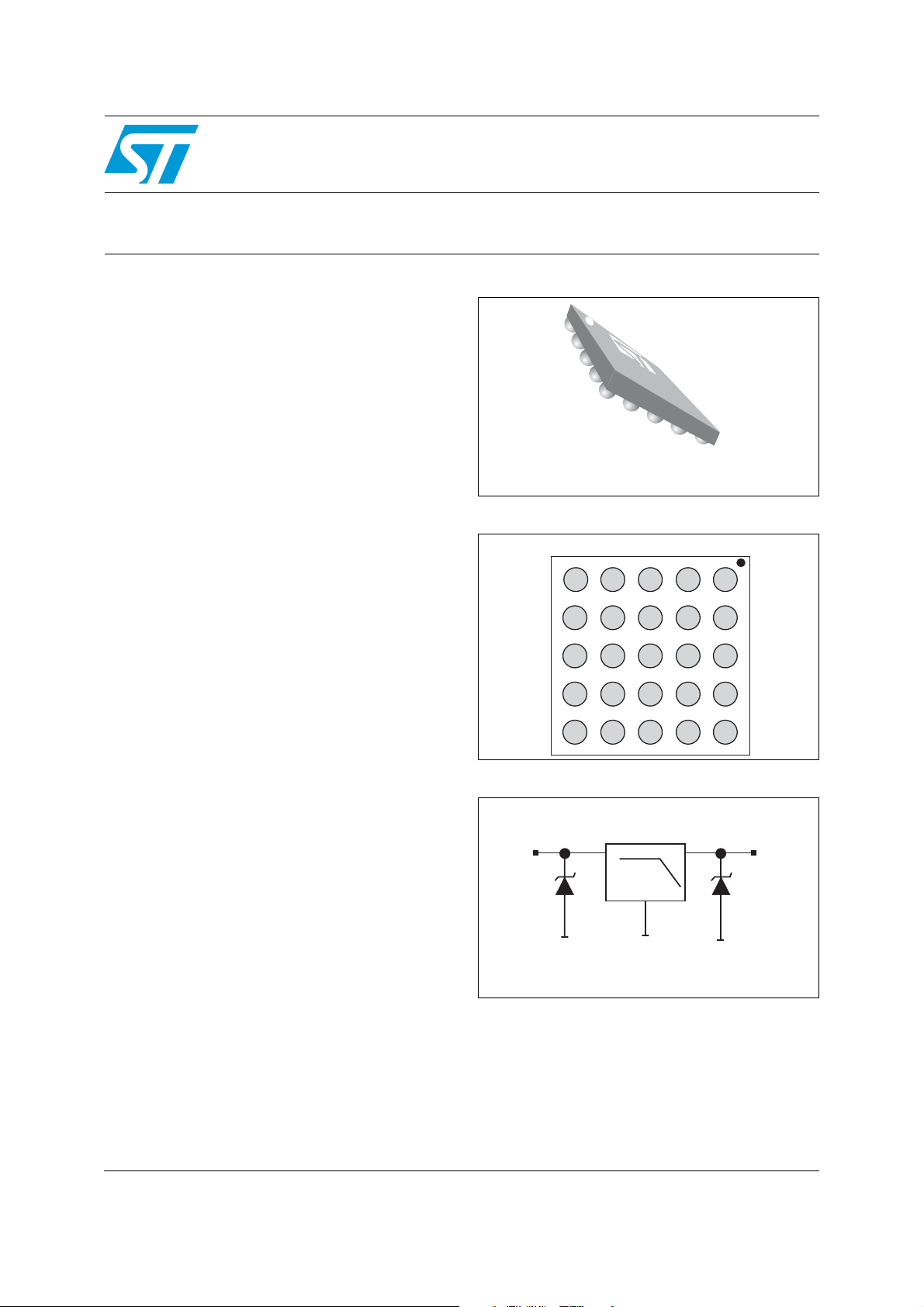
10-line IPAD™, EMI filter including ESD protection
Features
■ EMI symmetrical (I/O) low-pass filter
■ Lead free package
■ Very low PCB space consuming: < 6 mm
■
Very thin package: 0.65 mm
■ High efficiency in ESD suppression on both
input & output pins
■ High reliability offered by monolithic integration
2
EMIF10-COM01F2
Flip Chip
(25 bumps)
Complies with the following standard:
■ IEC 61000-4-2 level 4
– 15 kV (air discharge)
– 8 kV (contact discharge)
Applications
EMI filtering and ESD protection for:
■ Computers and printers
■ Communication systems
■ Mobile phones
Description
The EMIF10-COM01F2 is a highly integrated
device designed to suppress EMI / RFI noise in all
systems subjected to electromagnetic
interferences. The EMIF10 Flip-Chip packaging
means the package size is equal to the die size.
Additionally, this filter includes an ESD protection
circuitry which prevents damage to the application
when subjected to ESD surges up to 15 kV.
Figure 1. Pin configuration (bump side)
54
I5
3
21
I3
I9 I8I10
GNDGND
I1
I2I4
I6
I7
GNDGND GND
0609 08010 07
0204 0305
01
A
B
C
D
E
Figure 2. Basic cell configuration
Low-pass Filter
Input
R = 200
I/O
C = 45 pF
line
Ω
Output
TM: IPAD is a trademark of STMicroelectronics.
April 2008 Rev 5 1/7
www.st.com
7
Page 2
Characteristics EMIF10-COM01F2
1 Characteristics
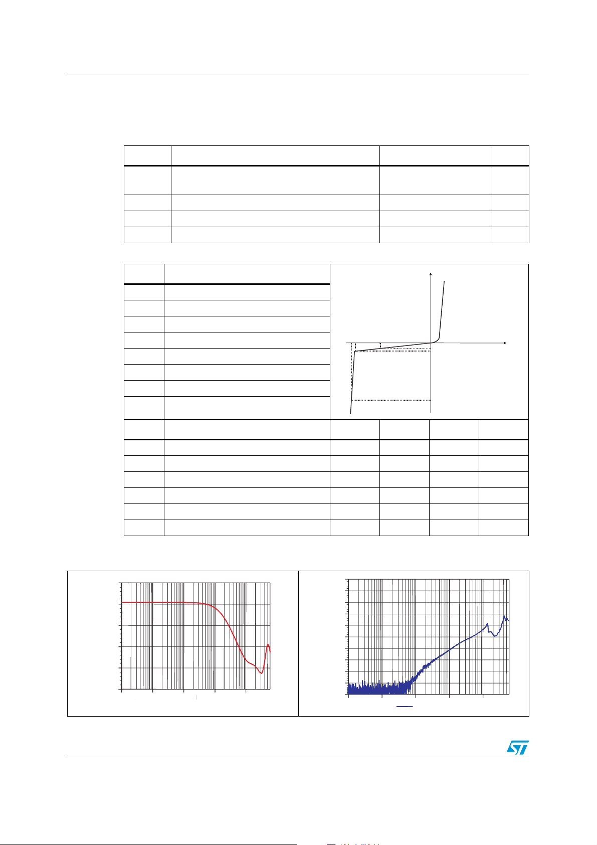
Table 1. Absolute ratings (T
Symbol Parameter and test conditions Value Unit
amb
= 25 °C)
V
T
T
Table 2. Electrical characteristics (T
ESD discharge IEC61000-4-2, air discharge
PP
ESD discharge IEC61000-4-2, contact discharge
Junction temperature 125 °C
T
j
Operating temperature range - 40 to + 85 °C
op
Storage temperature range - 55 to + 150 °C
stg
Symbol Parameter
V
V
V
R
C
Breakdown voltage
BR
I
Leakage current @ V
RM
Stand-off voltage
RM
Clamping voltage
CL
R
Dynamic impedance
d
I
Peak pulse current
PP
Resistance between Input and Output
I/O
Input capacitance per line
line
Symbol Test conditions Min. Typ. Max. Unit
V
BRIR
I
RM
R
R
I/O
C
line
t
LH
= 1 mA 6 8 10 V
VRM = 3 V per line 500 nA
IPP = 10 A, tp = 2.5 µs 1 Ω
d
At 0 V bias 45 50 pF
V
= 2.8 V R
input
Figure 3. S21(db) attenuation
measurement
0.00
0.00
0.00
dB
dB
dB
-10.00
-10.00
-10.00
-20.00
-20.00
-20.00
-30.00
-30.00
-30.00
-40.00
-40.00
-40.00
-50.00
-50.00
-50.00
100.0k 1.0M 10.0M 100.0M 1.0G
100.0k 1.0M 10.0M 100.0M 1.0G
100.0k 1.0M 10.0M 100.0M 1.0G
(1)
f/Hz
f/Hz
f/Hz
amb
15
8
= 25 °C)
kV
I
RM
V
CL
V
V
RM
BR
slope : 1 / R d
I
RM
I
R
I
PP
V
180 200 220 Ω
= 100 kΩ 25 ns
load
Figure 4. Analog crosstalk
0.00
0.00
dB
dB
-10.00
-10.00
-20.00
-20.00
-30.00
-30.00
-40.00
-40.00
-50.00
-50.00
-60.00
-60.00
-70.00
-70.00
-80.00
-80.00
-90.00
-90.00
-100.00
-100.00
100.0k 1.0M 10.0M 100.0M 1.0G
100.0k 1.0M 10.0M 100.0M 1.0G
Xtalk 1/2
f/Hz
f/Hz
1. Spikes at high frequencies are induced by the PCB layout
2/7
Page 3
EMIF10-COM01F2 Characteristics
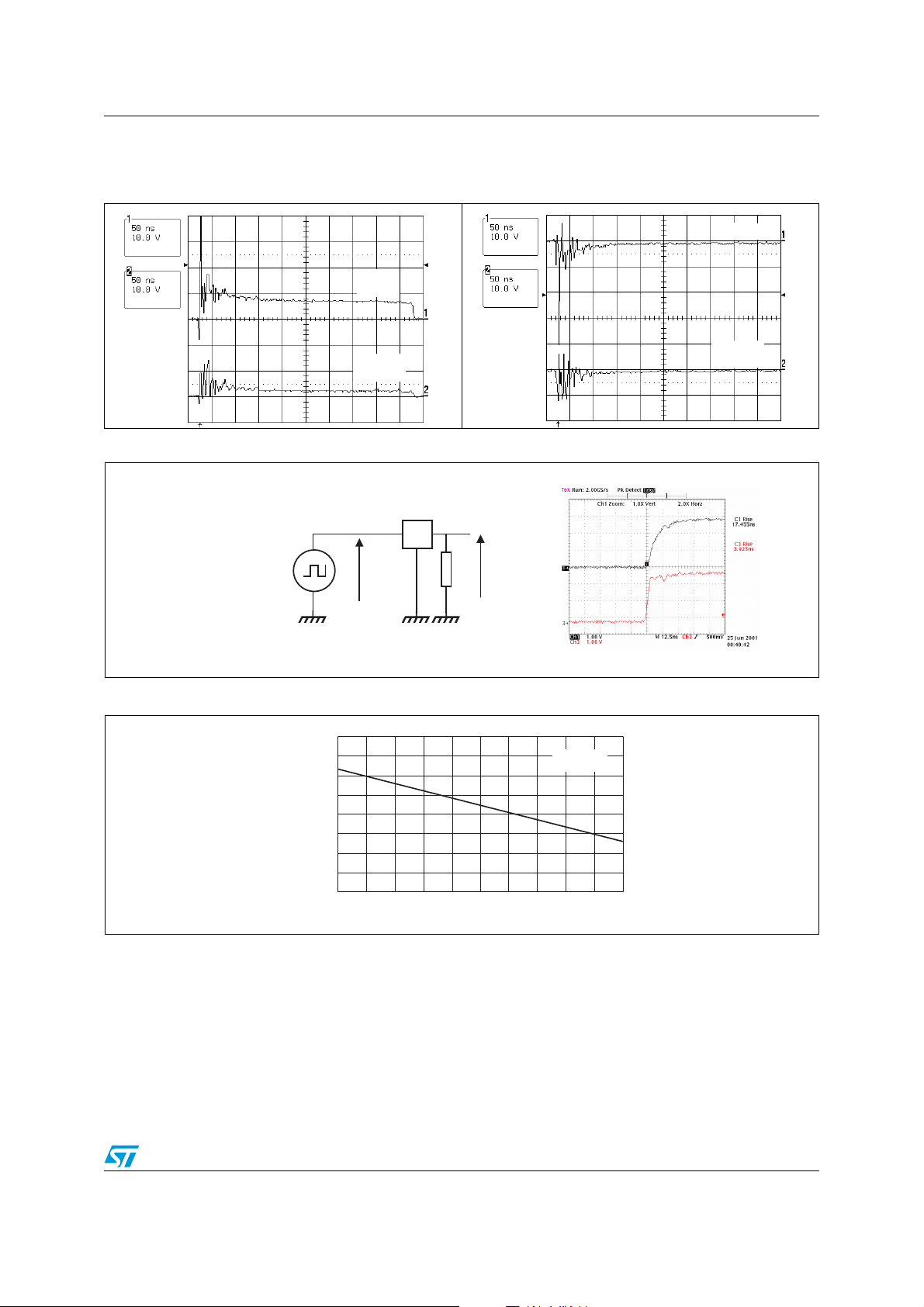
Figure 5. ESD response to IEC 61000-4-2
(+15 kV air discharge) on one input
) and on one output (V
(V
in
V(out1)
V(in1)
out
)
Figure 7. Rise time measurement
EMIF10-COM01F2
In Out
Square signal
Generator Vc = 2.8V
Vin
Figure 6. ESD response to IEC 61000-4-2
(-15 kV air discharge) on one input
100k
(Vin) and on one output (V
Vout
out
V(in1)
V(out1)
)
Figure 8. Capacitance versus reverse applied voltage
C(pF)
50
40
30
20
10
012345
VR(V)
F=1MHz
Vosc=30mV
3/7
Page 4
Application information EMIF10-COM01F2
2 Application information
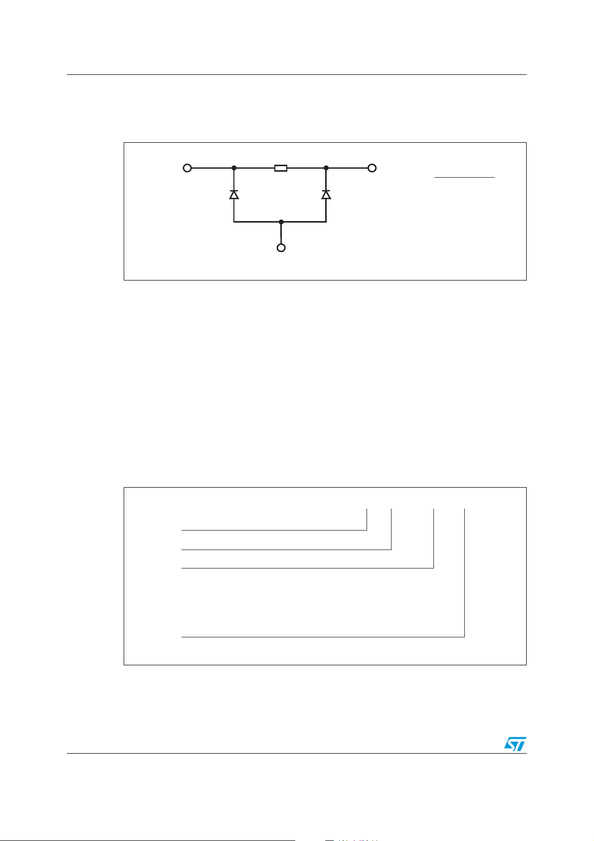
Figure 9. Aplac model
in
200R
MODEL = demif10 MODEL = demif10
sub
2.1 PCB grounding recommendations
In order to ensure a good efficiency in terms of ESD protection and filtering behavior, we
recommend to implement microvias (100 µm dia.) between the GND bumps and the GND
layer. GND bumps can be connected together in PCB layer 1, and in addition, if possible,
use through hole vias (200 µm dia.) in both sides of filter to improve contact to GND (layer).
This layout will minimize the distance to the ground and thus parasitic inductances. In
addition, we recommend to have GND plane wherever possible.
3 Ordering information scheme
out
Demif10 model
BV = 7
IBV = 1m
CJO = 25p
M = 0.3333
RS = 1
VJ = 0.6
TT = 100n
Figure 10. Ordering information scheme
EMI Filter
Number of lines
Information
x = resistance value (Ohms)
z = capacitance value / 10(pF)
or
3 letters = application
2 digits = version
Package
F = Flip Chip
x = 2: Lead-free, pitch = 500 µm, bump = 315 µm
4/7
EMIF yy - xxx zz Fx
Page 5
EMIF10-COM01F2 Package information
4 Package information
In order to meet environmental requirements, ST offers these devices in ECOPACK®
packages. These packages have a lead-free second level interconnect. The category of
second level interconnect is marked on the inner box label, in compliance with JEDEC
Standard JESD97. The maximum ratings related to soldering conditions are also marked on
the inner box label. ECOPACK is an ST trademark. ECOPACK specifications are available at
www.st.com.
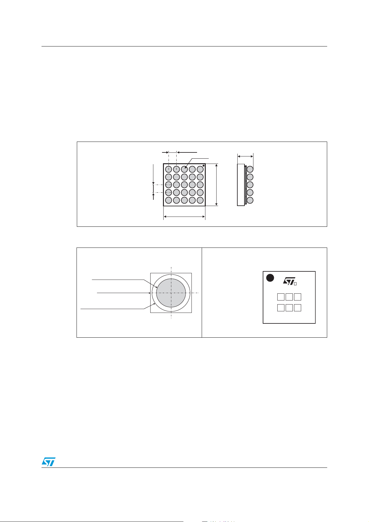
Figure 11. Flip Chip package dimensions
500 µm ± 50
315 µm ± 50
500 µm ± 50
2.39 mm ± 30 µm
2.39 mm ± 30 µm
650 µm ± 65
Figure 12. Footprint recommendations Figure 13. Marking
Dot, ST logo
xx = marking
z = manufacturing location
Copper pad Diameter:
250 µm recommended, 300 µm max
Solder stencil opening: 330 µm
Solder mask opening recommendation:
340 µm min for 300 µm copper pad diameter
yww = datecode
(y = year
ww = week)
E
xyxwz
w
5/7
Page 6
Ordering information EMIF10-COM01F2
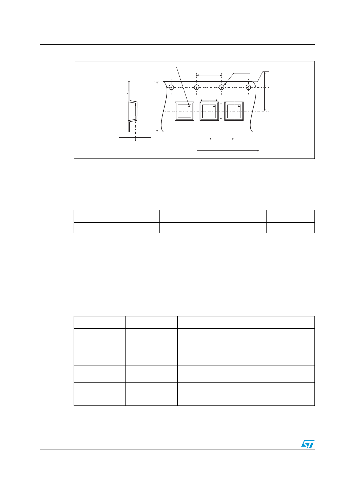
Figure 14. Flip Chip tape and reel specification
Dot identifying Pin A1 location
4 ± 0.1
Ø 1.5 ± 0.1
1.75 ± 0.1 3.5 ± 0.1
8 ± 0.3
0.73 ± 0.05
All dimensions in mm
yww
ST
xxz
E
2.6
yww
xxz
User direction of unreeling
5 Ordering information
Table 3. Ordering information
Order code Marking Package Weight Base qty Delivery mode
EMIF10-COM01F2 FE Flip Chip 8.3 mg 5000 Tape and reel
Note: More information is available in the application notes:
AN1235: “Flip Chip: Package description and recommendations for use”
AN1751: "EMI Filters: Recommendations and measurements"
ST
E
4 ± 0.1
ST
yww
xxz
2.6
E
6 Revision history
Table 4. Document revision history
Date Revision Description of changes
14-Dec-2004 1 First issue.
08-Apr-2005 2 Die shrink.
19-Oct-2005 3
03-Apr-2006 4
17-Apr-2008 5
6/7
Replaced Figures 3 and 13. Added ECOPACK
statement.
Reformatted to current standard. Pin identification in
Figure 1 updated.
Updated ECOPACK statement. Updated Figure 10,
Figure 11 and Figure 14. Reformatted to current
standards.
Page 7

EMIF10-COM01F2
Please Read Carefully:
Information in this document is provided solely in connection with ST products. STMicroelectronics NV and its subsidiaries (“ST”) reserve the
right to make changes, corrections, modifications or improvements, to this document, and the products and services described herein at any
time, without notice.
All ST products are sold pursuant to ST’s terms and conditions of sale.
Purchasers are solely responsible for the choice, selection and use of the ST products and services described herein, and ST assumes no
liability whatsoever relating to the choice, selection or use of the ST products and services described herein.
No license, express or implied, by estoppel or otherwise, to any intellectual property rights is granted under this document. If any part of this
document refers to any third party products or services it shall not be deemed a license grant by ST for the use of such third party products
or services, or any intellectual property contained therein or considered as a warranty covering the use in any manner whatsoever of such
third party products or services or any intellectual property contained therein.
UNLESS OTHERWISE SET FORTH IN ST’S TERMS AND CONDITIONS OF SALE ST DISCLAIMS ANY EXPRESS OR IMPLIED
WARRANTY WITH RESPECT TO THE USE AND/OR SALE OF ST PRODUCTS INCLUDING WITHOUT LIMITATION IMPLIED
WARRANTIES OF MERCHANTABILITY, FITNESS FOR A PARTICULAR PURPOSE (AND THEIR EQUIVALENTS UNDER THE LAWS
OF ANY JURISDICTION), OR INFRINGEMENT OF ANY PATENT, COPYRIGHT OR OTHER INTELLECTUAL PROPERTY RIGHT.
UNLESS EXPRESSLY APPROVED IN WRITING BY AN AUTHORIZE REPRESENTATIVE OF ST, ST PRODUCTS ARE NOT DESIGNED,
AUTHORIZED OR WARRANTED FOR USE IN MILITARY, AIR CRAFT, SPACE, LIFE SAVING, OR LIFE SUSTAINING APPLICATIONS,
NOR IN PRODUCTS OR SYSTEMS, WHERE FAILURE OR MALFUNCTION MAY RESULT IN PERSONAL INJURY, DEATH, OR
SEVERE PROPERTY OR ENVIRONMENTAL DAMAGE.
Resale of ST products with provisions different from the statements and/or technical features set forth in this document shall immediately void
any warranty granted by ST for the ST product or service described herein and shall not create or extend in any manner whatsoever, any
liability of ST.
ST and the ST logo are trademarks or registered trademarks of ST in various countries.
Information in this document supersedes and replaces all information previously supplied.
The ST logo is a registered trademark of STMicroelectronics. All other names are the property of their respective owners.
© 2008 STMicroelectronics - All rights reserved
STMicroelectronics group of companies
Australia - Belgium - Brazil - Canada - China - Czech Republic - Finland - France - Germany - Hong Kong - India - Israel - Italy - Japan -
Malaysia - Malta - Morocco - Singapore - Spain - Sweden - Switzerland - United Kingdom - United States of America
www.st.com
7/7
 Loading...