

Page 1
®
IPAD
TM
MAIN APPLICATION
MULTIMEDIACARD™
■
DESCRIPTION
TheEMIF04-MMC02F1 isa highly integratedarray
designed to suppress EMI / RFI noise for
MULTIMEDIACARD™ port filtering.
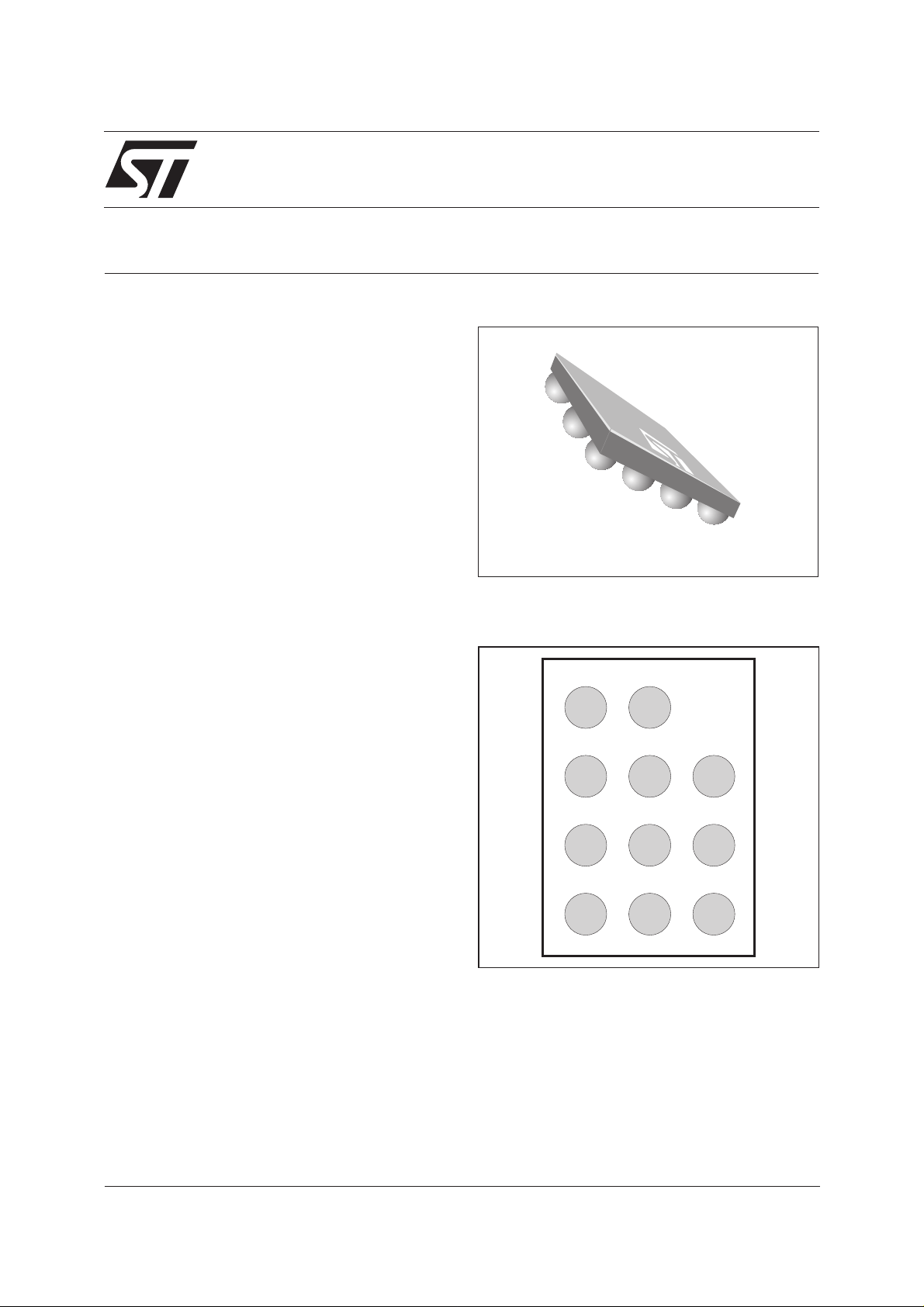
TheEMIF04-MMC02F1 flip-chippackaging means
the package size is equal to the die size. That's
why EMIF04-MMC02F1 is a very small device.
Additionally, this filter includes an ESD protection
circuitry which prevents the protected device from
destruction when subjected to ESD surges up to
15 kV.
EMIF04-MMC02F1
4 LINES EMI FILTER
INCLUDING ESD PROTECTION
Flip Chip package
PIN CONFIGURATION
BENEFITS
■ 4 lines low-pass-filter
■ High efficiency in EMI filtering
■
Very low PCB space consuming:< 3.3 mm
■
Very thin package: 0.65 mm
■
High efficiency in ESD suppression
2
(IEC61000-4-2 level 4)
■
High reliability offered by monolithic integration
■
High reducing of parasitic elements through
integration & wafer level packaging.
COMPLIES WITH THEFOLLOWING STANDARDS:
IEC 61000-4-2 Level 4:
15kV (air discharge)
8 kV (contact discharge)
on input & output pins.
MIL STD 883E- Method 3015-6 Class 3
A3
B3
C3
D3
A2
B2
C2
D2
B1
C1
D1
TM : IPAD is a trademark of STMicroelectronics.
September 2002 - Ed: 4A
1/6
Page 2
EMIF04-MMC02F1
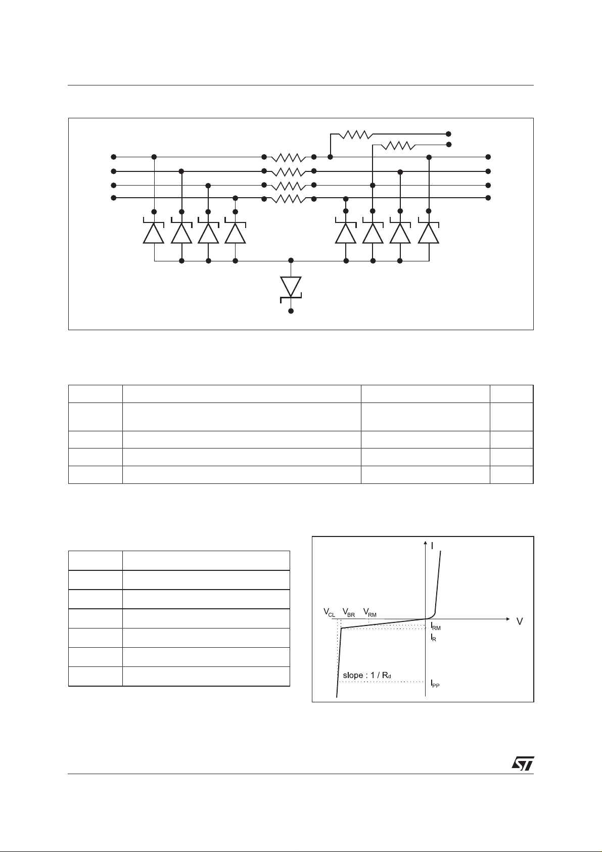
SCHEMATIC
A3
B3
C3
D3
ABSOLUTE MAXIMUM RATINGS (T
amb
R10
R20
R1
R2
R3
R4
D2
GND
=25°C)
C2
B2
A2
B1
C1
D1
Symbol Parameter and test conditions Value Unit
V
PP
ESD discharge IEC61000-4-2, air discharge
ESD discharge IEC61000-4-2, contact discharge
15
8
kV
T
j
T
op
T
stg
Junction temperature
Operating temperature range
Storage temperature range
ELECTRICAL CHARACTERISTICS (T
Symbol Parameter
V
I
V
V
BR
RM
RM
CL
Rd
I
PP
Breakdown voltage
Leakage current @ V
Stand-off voltage
Clamping voltage
Dynamic impedance
Peak pulse current
RM
amb
125 °C
-40 to + 85 °C
-55 to +150 °C
=25°C)
2/6
Page 3
EMIF04-MMC02F1
Symbol Test conditions Min. Typ. Max. Unit
V
BR
I
RM
C
line
R
1,R2,R3,R4
R
10
R
20
IR=1mA
VRM=3V
@0V
Tolerance ± 5%
Tolerance ± 5%
Tolerance ± 5%
P 70 mW
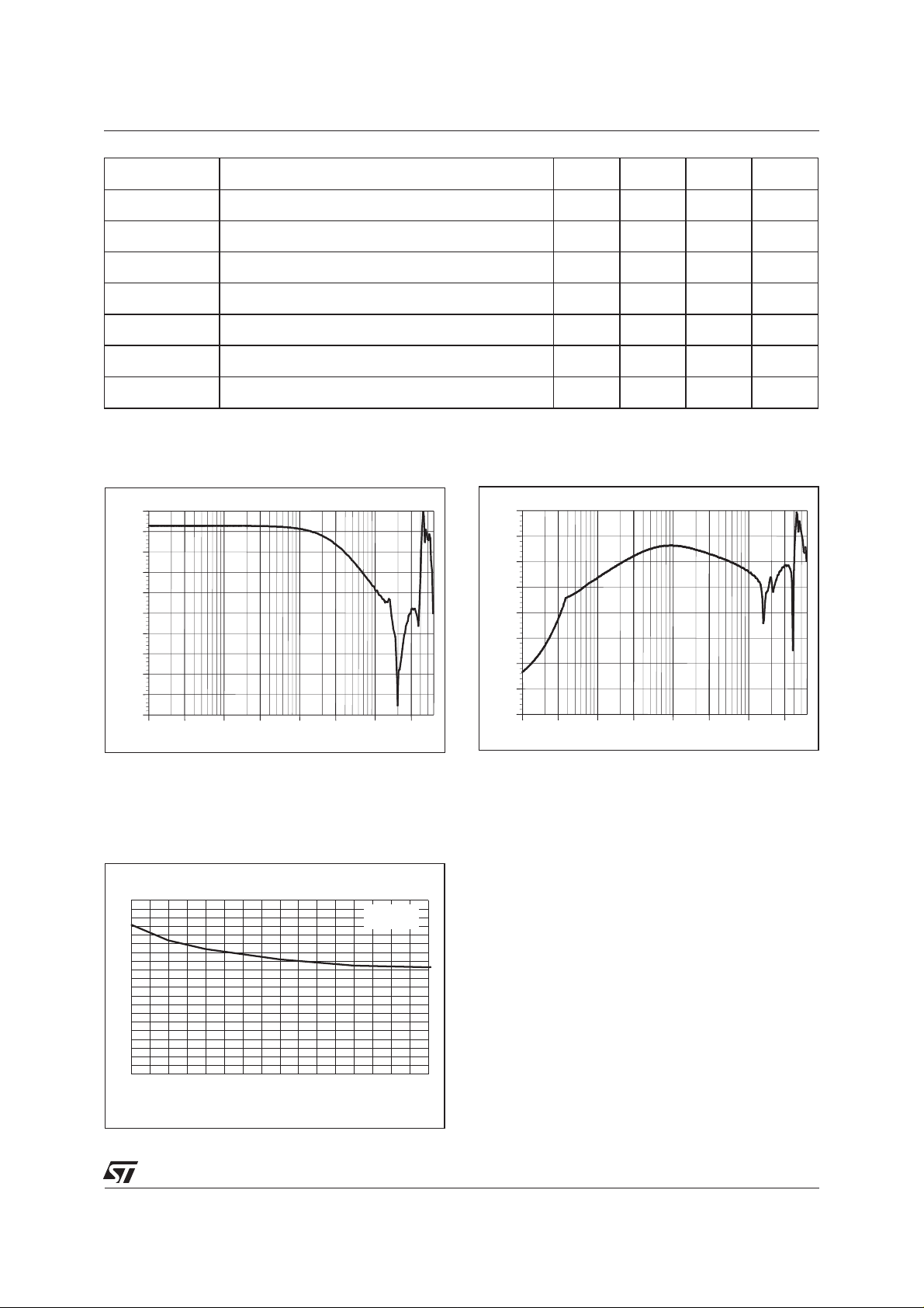
Fig. 1: Filtering measurements
S21(dB) measurements of C3/C1 line
0.00
dB
-5.00
-10.00
-15.00
-20.00
-25.00
-30.00
-35.00
-40.00
-45.00
-50.00
1.0M 3.0M 10.0M 30.0M 100.0M 300.0M 1.0G 3.0G
f/Hz
6V
0.1 0.5 µA
20 pF
47 Ω
13 kΩ
56 kΩ
Fig. 2: Cross talk measurements
Xtalk measurements C3/B1
0.00
dB
-10.00
-20.00
-30.00
-40.00
-50.00
-60.00
-70.00
-80.00
1.0M 3.0M 10.0M 30.0M 100.0M 300.0M 1.0G 3.0G
f/Hz
Note: spikes at high frequencies are induced by the PCB
layout.
Fig. 3: Line capacitance versus reverse applied
voltage.
C(pF)
20
18
16
14
12
10
8
6
4
2
0
0.0 0.5 1.0 1.5 2.0 2.5 3.0 3.5 4.0
V
(V)
R
V
F=1MHz
osc
Tj=25°C
=30mV
RMS
3/9
Page 4

EMIF04-MMC02F1
Fig. 4: ESD response to IEC61000-4-2 (+15kV contact discharge).
Positive Surge
Negative Surge
APLAC MODEL
Fig. 5: Device structure
R10R20
A3
B3
C3
D3
MODEL = demif04 MODEL = demif04
R1
R2
R3
R4
B2
C2
A2
B1
C1
D1
4/9
MODEL = demif04_gnd
D2
120pH
100m
DEMIF04
BV = 7
IBV = 1m
CJO = Cz
M = 0.3333
RS = 1
VJ = 0.6
TT = 100n
DEMIF04 gnd
BV = 7
IBV = 1m
CJO = Cz_gnd
M = 0.3333
RS = 1
VJ = 0.6
TT = 100n
Page 5

EMIF04-MMC02F1
Fig. 6: Aplac model connections
A3
B3
C3
D3
Cins
Cins
Cins
Cins
Rins
Rins
Rins
Rins
Rins
Cins
cap_hole
D2
Lbump
Rbump
Lhole
Rhole
Rins
Rins
Rins
Rins
Rins
Cins
Cins
Cins
Cins
Cins
A2
B1
C1
D1
aplacvar R1 47 opt
aplacvar R2 47
aplacvar R3 47
aplacvar R4 47
aplacvar R10 13k
aplacvar R20 56k
aplacvar Cz 15pF opt
aplacvar Cz_gnd 45pF opt
aplacvar Ls 450pH opt
aplacvar Rs 300m
aplacvar Rbump 50m
aplacvar Lbump 50pH
aplacvar lhole 940pH opt
aplacvar Rhole 100m
aplacvar cap_hole 0.15pF
aplacvar Cins 200fF
aplacvar Rins 10Meg
5/6
Page 6

EMIF04-MMC02F1
Fig. 7: Aplac simulation versus frequency
measurement.
0.00
dB
-5.00
-10.00
-15.00
-20.00
-25.00
-30.00
-
-35.00
-40.00
-
-45.00
-50.00
1.0M 3.0M 10.0M 30.0M 100.0M 300.0M 1.0G 3.0G
EMIF04-MMC02F1: Aplac vs measurement (C3/C1 line)
Measurement
f/Hz
ORDER CODE
EMIF 04 - MMC 02 F 1
Electro Magnetic
Interference Filter
Nb of lines
Simulation
Pitch and Bump version
1: pitch = 0.5mm
bump = 0.3mm
FLIP CHIP
Version
PACKAGE MECHANICAL DATA
500 ± 50
1570 ± 50
MULTIMEDIACARD™
port fonction
315 ± 50
2070 ± 50
All dimensions in µm
650 ± 65
6/6
Page 7

EMIF04-MMC02F1
MARKING
250
250
∅ 230
2070
200
F HT
YWW
®
220
40
PACKING
0.73 +/- 0.05
Dot identifying Pin A1 location*
8 +/- 0.3
All dimensions in mm
yww
4 +/- 0.1
yww
FHT
ST
User direction of unreeling
1.5 +/- 0.1
yww
FHT
FHT
ST
ST
4 +/- 0.1
1570
- yww: Date code
OTHER INFORMATION
Ordering code Marking Package Weight Base qty Delivery mode
EMIF04-MMC02F1 FHT Flip-Chip 4.5 mg 5000 Tape & reel (7”)
1.75 +/- 0.1
3.5 +/- 0.1
Note: More packing informations are available in the application note AN1235: ''Flip-Chip: Package description and
recommandations for use''
Informationfurnishedisbelievedtobeaccurateandreliable.However,STMicroelectronicsassumesnoresponsibilityfortheconsequences of
useofsuch information nor for any infringement of patents or other rights of third parties which may result from its use. No license is granted by
implication or otherwise under any patent or patent rights of STMicroelectronics. Specifications mentioned in this publication are subject to
change without notice. This publication supersedes and replaces all information previously supplied.
STMicroelectronics products are not authorized for use as critical components in life support devices or systems without express written approval of STMicroelectronics.
The ST logo is a registered trademark of STMicroelectronics
© 2002 STMicroelectronics - Printed in Italy - All rights reserved.
STMicroelectronics GROUP OF COMPANIES
Australia - Brazil - Canada - China - Finland - France - Germany
Hong Kong - India - Israel - Italy - Japan - Malaysia - Malta - Morocco - Singapore
Spain - Sweden - Switzerland - United Kingdom - United States.
http://www.st.com
7/6
 Loading...