

Page 1
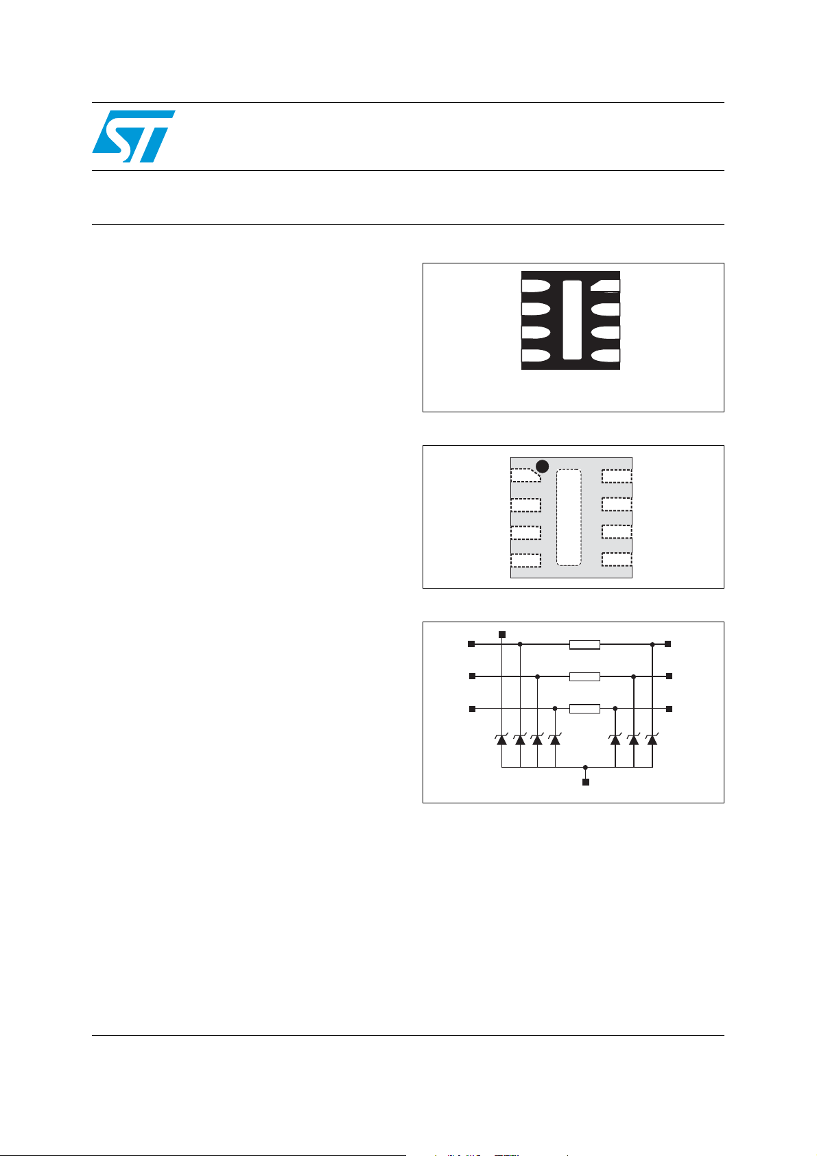
EMIF03-SIM02M8
3 line IPAD™, EMI filter for SIM card applications
Features
■ SIM card EMI low-pass filter
■ High efficiency in EMI filtering
■ Very low PCB space consumption:
1.7 mm x 1.5 mm
■ Very thin package: 0.6 mm max
■ High efficiency in ESD suppression on external
pins (IEC 61000-4-2 level 4).
■ High reliability offered by monolithic integration
■ High reduction of parasitic elements through
integration and wafer level packaging.
■ Lead free package
■ Easy layout and flexibility thanks to I/O
topology
■ Low clamping voltage
Complies with following standards
■ IEC 61000-4-2 level 4 external pins
– 15 kV (air discharge)
– 8 kV (contact discharge)
■ IEC 61000-4-2 level 2 internal pins
– 2 kV (air discharge)
– 2 kV (contact discharge)
■ MIL STD 883G - Method 3015-7 Class 3A (all
pins)
8
7
6
5
GND
GND
11
2
3
4
Micro QFN 1.7 mm x 1.5 mm
(bottom view)
Figure 1. Pin configuration (top view)
RST
CLK
Data
Vcc
in
in
in
GND
Vcc
RST
CLK
Data
EXT
EXT
EXT
Figure 2. Device configuration
RST in
CLK in
Data in
Vcc
100 Ω
R1
47 Ω
R2
100 Ω
R3
RST ext
CLK ext
Data ext
Applications
Maximum line capacitance = 20 pF
GND
Where EMI filtering in ESD sensitive equipment is
required:
■ Keyboard for mobile phones
■ Computers and printers
■ Communication systems
■ MCU boards
Description
The EMIF03-SIM02M8 is a 3 line highly
integrated device designed to suppress EMI/RFI
noise in all systems exposed to electromagnetic
interference.
This filter includes ESD protection circuitry, which
prevents damage to the application when
subjected to ESD surges up to 15 kV on the
TM: IPAD is a trademark of STMicroelectronics
October 2007 Rev 1 1/10
external pins.
www.st.com
Page 2
Characteristics EMIF03-SIM02M8
1 Characteristics
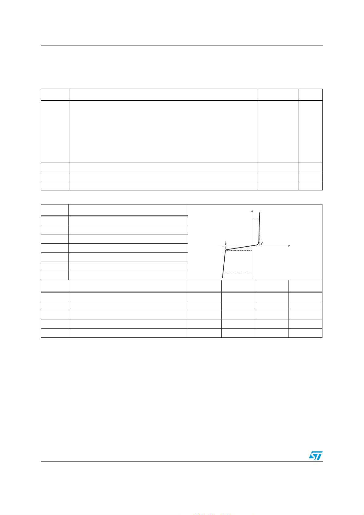
Table 1. Absolute ratings (limiting values at T
= 25 °C unless otherwise specified)
amb
Symbol Parameter Value Unit
Internal pins
ESD discharge IEC 61000-4-2 air discharge
ESD discharge IEC 61000-4-2 contact discharge
V
External pins and V
PP
ESD discharge IEC 61000-4-2 air discharge
CC
ESD discharge IEC 61000-4-2 contact discharge
2
2
15
8
All pins
MIL STD 883G - Method 3015-7 Class 3A (human body model)
Junction temperature 125 °C
T
j
T
T
Table 2. Electrical characteristics (T
Operating temperature range -40 to + 85 °C
op
Storage temperature range -55 to +150 °C
stg
Symbol Parameter
V
I
V
V
I
R
C
Breakdown voltage
BR
Leakage current @ V
RM
Stand-off voltage
RM
Clamping voltage
CL
Peak pulse current
PP
Series resistance between input and output
I/O
Input capacitance per line
line
RM
amb
= 25 °C)
I
I
F
V
BR
V
V
RM
CL
I
RM
I
R
I
PP
4
V
F
V
Symbol Test conditions Min. Typ. Max. Unit
V
I
R
1
R
C
IR = 1 mA 6 7.9 V
BR
VRM = 3 V 0.2 µA
RM
, R3Tolerance ± 20% 100 Ω
Tolerance ± 20% 47 Ω
2
VR= 0 V, F = 1 MHz, V
line
= 30 mV 17 20 pF
OSC
kV
2/10
Page 3
EMIF03-SIM02M8 Characteristics
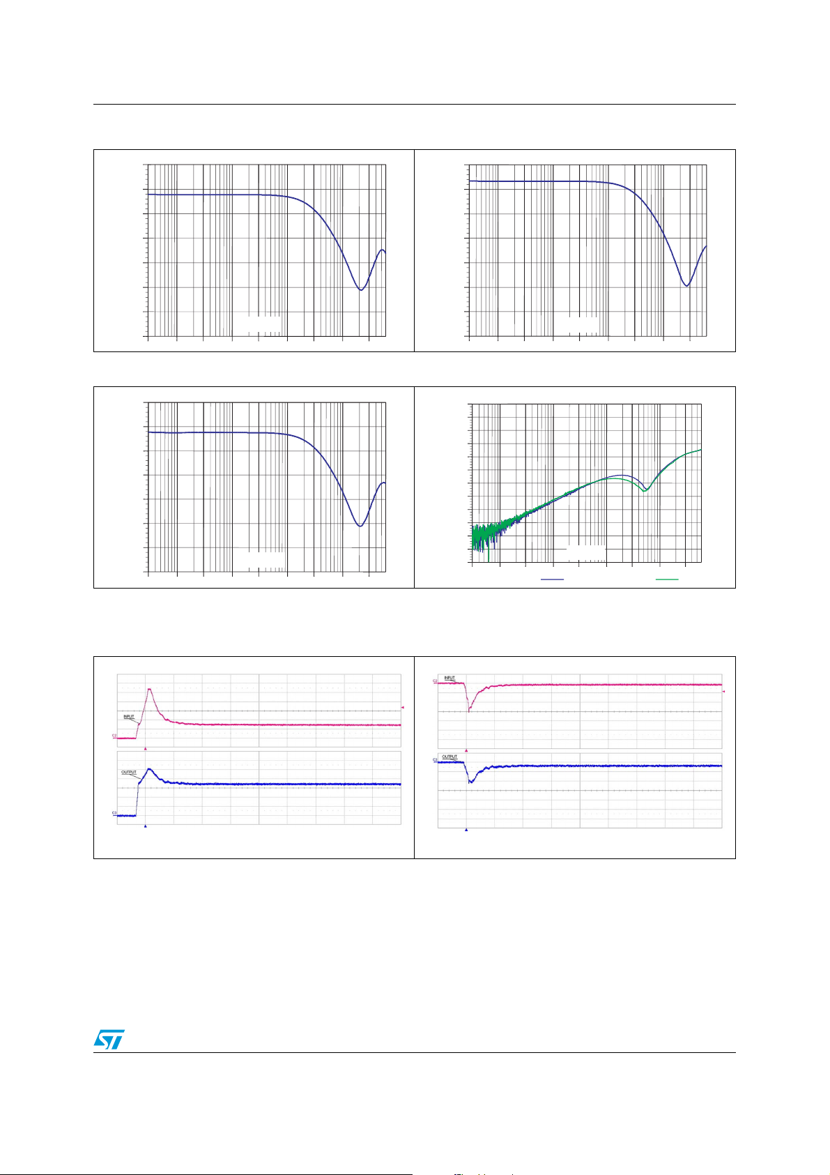
Figure 3. S21(db) attenuation (RST line) Figure 4. S21(db) attenuation (CLK line)
dB
0.00
-5.00
-10.00
-15.00
-20.00
-25.00
-30.00
F (Hz)
-35.00
300.0k 1.0M 3.0M 10.0M 30.0M 100.0M 300.0M 1.0G 3.0G
dB
0.00
-5.00
-10.00
-15.00
-20.00
-25.00
-30.00
-35.00
300.0k 1.0M 3.0M 10.0M 30.0M 100.0M 300.0M 1.0G 3.0G
F (Hz)
Figure 5. S21(db) attenuation (DATA line) Figure 6. Analog cross talk measurements
dB
0.00
-5.00
-10.00
-15.00
-20.00
-25.00
-30.00
F (Hz)
-35.00
300.0k 1.0M 3.0M 10.0M 30.0M 100.0M 300.0M 1.0G 3.0G
Figure 7. ESD response to IEC 61000-4-2
(+15 kV air discharge) applied to
external pin
Figure 8. ESD response to IEC 61000-4-2
dB
0.00
-10.00
-20.00
-30.00
-40.00
-50.00
-60.00
-70.00
-80.00
-90.00
-100.00
-110.00
-120.00
300.0k 1.0M 3.0M 10.0M 30.0M 100.0M 300.0M 1.0G 3.0G
ClkIn- RstExt DataIn-Rst/Clk
F (Hz)
(-15 kV air discharge) applied to
external pin
5 V/div
2 V/div
200 ns/div
5 V/div
2 V/div
200 ns/div
3/10
Page 4
Application schematic EMIF03-SIM02M8
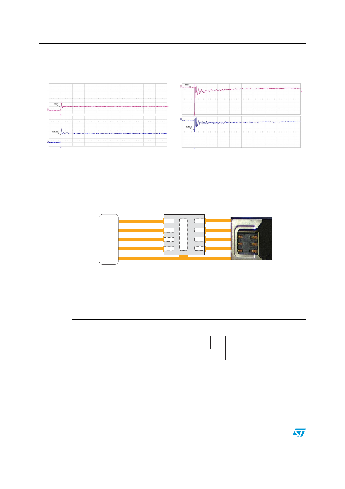
Figure 9. ESD response to IEC 61000-4-2
(+2 kV air discharge) applied to
internal pin
5 V/div
2 V/div
20 ns/div
2 Application schematic
Figure 11. Application schematic
Vcc
RST
in
CLK
in
Data
in
Figure 10. ESD response to IEC 61000-4-2
(-2 kV air discharge) applied to
internal pin
5 V/div
2 V/div
20 ns/div
Vcc
RST
EXT
CLK
GND
Data
EXT
EXT
SIM PROCESSOR
3 Ordering information scheme
Figure 12. Ordering information scheme
EMI Filter
Number of lines
Information
xxx = application
zz = version
Package
Mx = Micro QFN x leads
SIM CONNECTOR
EMIF yy - xxx zz Mx
4/10
Page 5
EMIF03-SIM02M8 Package information
4 Package information
● Epoxy meets UL94, V0
In order to meet environmental requirements, ST offers these devices in ECOPACK®
packages. These packages have a lead-free second level interconnect. The category of
second level interconnect is marked on the inner box label, in compliance with JEDEC
Standard JESD97. The maximum ratings related to soldering conditions are also marked on
the inner box label. ECOPACK is an ST trademark. ECOPACK specifications are available
at: www.st.com.
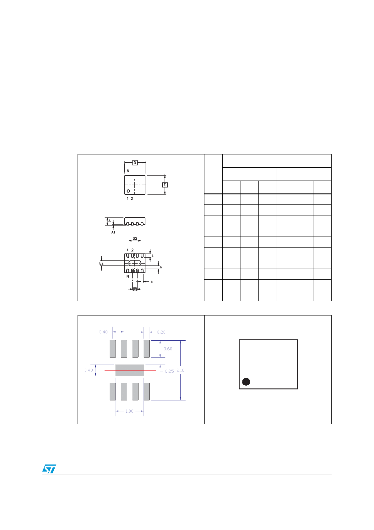
Table 3. QFN 1.7 x 1.5 package dimensions
Dimensions
Ref
A 0.50 0.55 0.60 0.20 0.22 0.24
A1 0.00 0.02 0.05 0.00 0.01 0.02
b 0.15 0.18 0.25 0.06 0.07 0.10
D 1.70 0.67
D2 0.9 1.00 1.10 0.35 0.39 0.43
E 1.50 0.59
E2 0.30 0.40 0.50 0.12 0.16 0.24
e 0.40 0.16
k 0.20 0.08
L 0.25 0.30 0.35 0.10 0.12 0.14
Millimeters inches
MIN TYP MAX MIN TYP MAX
Figure 13. Footprint (dimensions in mm) Figure 14. Marking
HA
Dot: Pin 1 Identification
5/10
Page 6
Package information EMIF03-SIM02M8
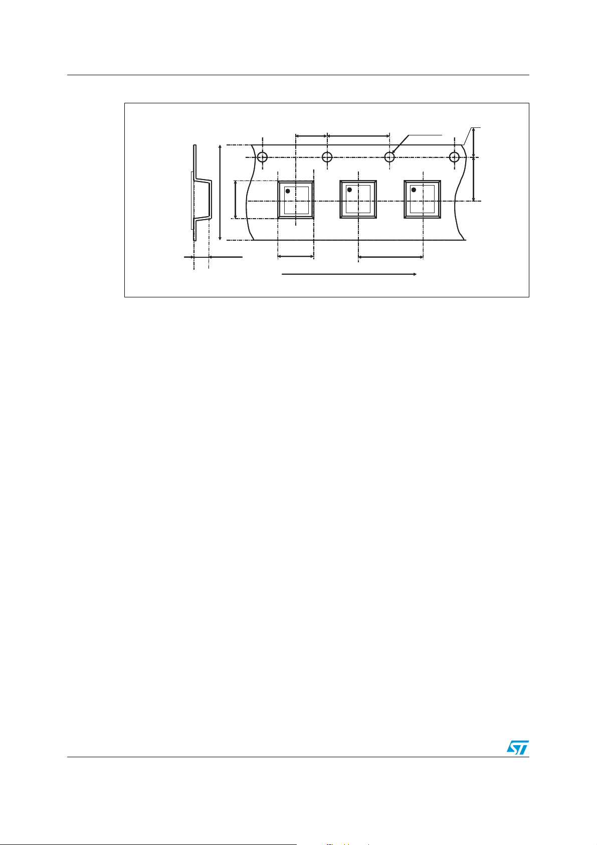
Figure 15. Tape and reel specification
1.75 +/- 0.1
4.00+/-0.1
2.0+/-0.05
2.0+/-0.05
8.0 +/- 0.3
8.0 +/- 0.3
1.90
1.90
XX
4.00+/-0.1
XX
φ 1.5 +/- 0.1
φ 1.5 +/- 0.1
XX
1.75 +/- 0.1
3.5 +/- 0.03
3.5 +/- 0.03
0.75 1.70
0.75 1.70
User direction of unreeling
User direction of unreeling
4.00
4.00
Note: Product marking may be rotated by 90° for assembly plant differentiation. In no case should
this product marking be used to orient the component for its placement on a PCB. Only pin
1 mark is to be used for this purpose.
6/10
Page 7
EMIF03-SIM02M8 Recommendation on PCB assembly
5 Recommendation on PCB assembly
5.1 Stencil opening design
1. General recommendation on stencil opening design
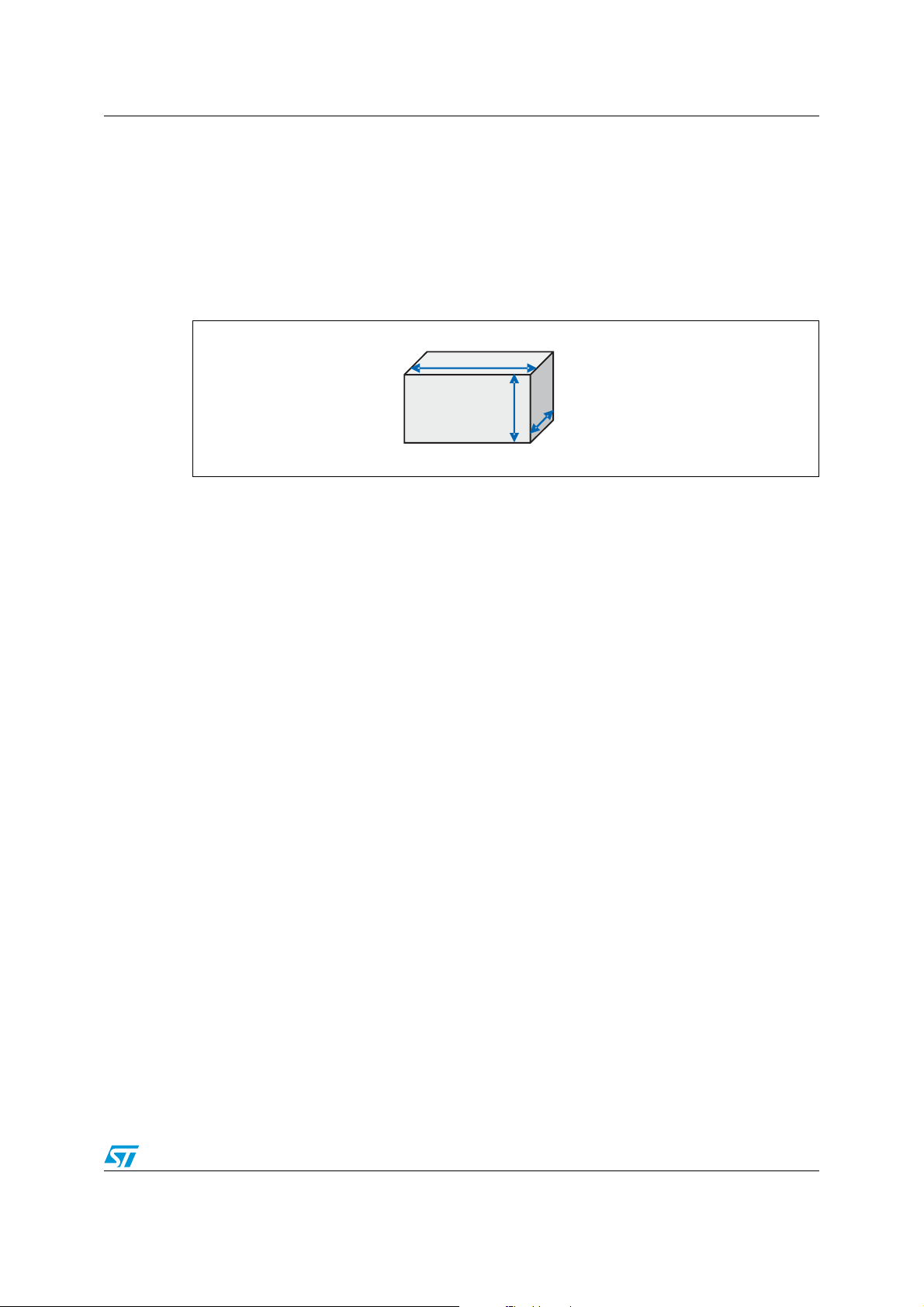
a) Stencil opening dimensions: L (Length), W (Width), T (Thickness).
Figure 16. Stencil opening dimensions
L
T
W
b) General Design Rule
Stencil thickness (T) = 75 ~ 125 µm
W
Aspect Ratio
Aspect Area
-----
1.5≥=
T
LW×
---------------------------2T L W+()
0.66≥=
2. Reference design
a) Stencil opening thickness: 100 µm
b) Stencil opening for central exposed pad: Opening to footprint ratio is 50%.
Example: Stencil opening L = 680 µm, W = 300 µm
Footprint (see Figure 13) L = 1000 µm, W = 400 µm
c) Stencil opening for leads: Opening to footprint ratio is 90%.
Example: Stencil opening L = 570 µm, W = 190 µm
Footprint (see Figure 13) L = 600 µm, W = 200 µm
5.2 Solder paste
1. Halide-free flux qualification ROL0 according to ANSI/J-STD-004.
2. “No clean” solder paste is recommended.
3. Offers a high tack force to resist component movement during high speed
4. Solder paste with fine particles: powder particle size is 20-45 µm.
7/10
Page 8
Recommendation on PCB assembly EMIF03-SIM02M8
5.3 Placement
1. Manual positioning is not recommended.
2. It is recommended to use the lead recognition capabilities of the placement system, not
the outline centering
3. Standard tolerance of ± 0.05 mm is recommended.
4. 3.5 N placement force is recommended. Too much placement force can lead to
squeezed out solder paste and cause solder joints to short. Too low placement force
can lead to insufficient contact between package and solder paste that could cause
open solder joints or badly centered packages.
5. To improve the package placement accuracy, a bottom side optical control should be
performed with a high resolution tool.
6. For assembly, a perfect supporting of the PCB (all the more on flexible PCB) is
recommended during solder paste printing, pick and place and reflow soldering by
using optimized tools.
5.4 PCB design preference
1. To control the solder paste amount, the closed via is recommended instead of open
vias.
2. The position of tracks and open vias in the solder area should be well balanced. The
symmetrical layout is recommended, in case any tilt phenomena caused by
asymmetrical solder paste amount due to the solder flow away.
5.5 Reflow profile
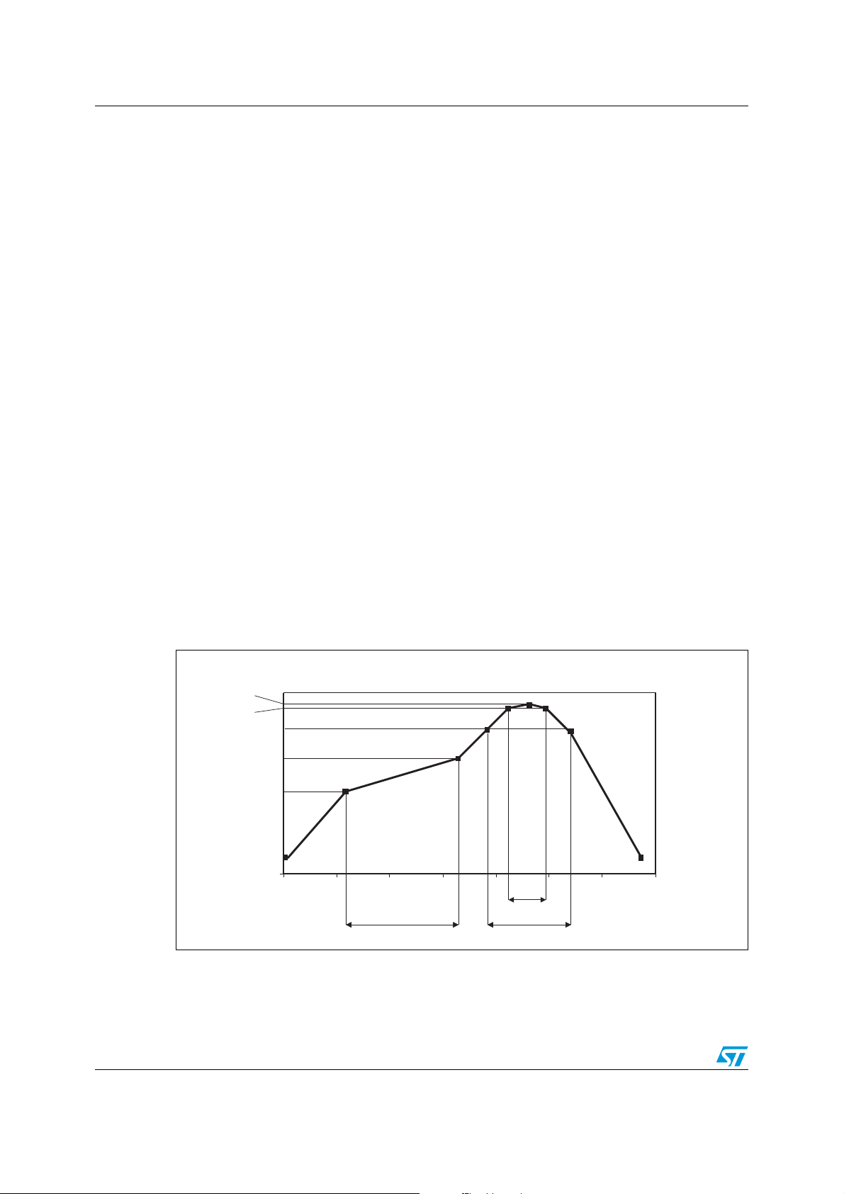
Figure 17. ST ECOPACK® recommended soldering reflow profile for PCB mounting
Temperature (°C)
Temperature (°C)
260°C max
260°C max
255°C
255°C
220°C
220°C
180°C
180°C
125 °C
125 °C
3°C/s max
3°C/s max
0
0
012345 67
012345 67
10-30 sec
10-30 sec
90 to 150 sec
90 to 150 sec
90 sec max
90 sec max
Note: Minimize air convection currents in the reflow oven to avoid component movement.
2°C/s recommended
2°C/s recommended
6°C/s max
6°C/s max
Time (min)
Time (min)
8/10
Page 9
EMIF03-SIM02M8 Ordering information
6 Ordering information
Table 4. Ordering information
Part number Marking Package Weight Base qty Delivery mode
EMIF03-SIM02M8 HA Micro QFN 4 mg 3000 Tape and reel (7”)
7 Revision history
Table 5. Document revision history
Date Revision Changes
07-Oct-2007 1 Initial release.
9/10
Page 10

EMIF03-SIM02M8
Please Read Carefully:
Information in this document is provided solely in connection with ST products. STMicroelectronics NV and its subsidiaries (“ST”) reserve the
right to make changes, corrections, modifications or improvements, to this document, and the products and services described herein at any
time, without notice.
All ST products are sold pursuant to ST’s terms and conditions of sale.
Purchasers are solely responsible for the choice, selection and use of the ST products and services described herein, and ST assumes no
liability whatsoever relating to the choice, selection or use of the ST products and services described herein.
No license, express or implied, by estoppel or otherwise, to any intellectual property rights is granted under this document. If any part of this
document refers to any third party products or services it shall not be deemed a license grant by ST for the use of such third party products
or services, or any intellectual property contained therein or considered as a warranty covering the use in any manner whatsoever of such
third party products or services or any intellectual property contained therein.
UNLESS OTHERWISE SET FORTH IN ST’S TERMS AND CONDITIONS OF SALE ST DISCLAIMS ANY EXPRESS OR IMPLIED
WARRANTY WITH RESPECT TO THE USE AND/OR SALE OF ST PRODUCTS INCLUDING WITHOUT LIMITATION IMPLIED
WARRANTIES OF MERCHANTABILITY, FITNESS FOR A PARTICULAR PURPOSE (AND THEIR EQUIVALENTS UNDER THE LAWS
OF ANY JURISDICTION), OR INFRINGEMENT OF ANY PATENT, COPYRIGHT OR OTHER INTELLECTUAL PROPERTY RIGHT.
UNLESS EXPRESSLY APPROVED IN WRITING BY AN AUTHORIZED ST REPRESENTATIVE, ST PRODUCTS ARE NOT
RECOMMENDED, AUTHORIZED OR WARRANTED FOR USE IN MILITARY, AIR CRAFT, SPACE, LIFE SAVING, OR LIFE SUSTAINING
APPLICATIONS, NOR IN PRODUCTS OR SYSTEMS WHERE FAILURE OR MALFUNCTION MAY RESULT IN PERSONAL INJURY,
DEATH, OR SEVERE PROPERTY OR ENVIRONMENTAL DAMAGE. ST PRODUCTS WHICH ARE NOT SPECIFIED AS "AUTOMOTIVE
GRADE" MAY ONLY BE USED IN AUTOMOTIVE APPLICATIONS AT USER’S OWN RISK.
Resale of ST products with provisions different from the statements and/or technical features set forth in this document shall immediately void
any warranty granted by ST for the ST product or service described herein and shall not create or extend in any manner whatsoever, any
liability of ST.
ST and the ST logo are trademarks or registered trademarks of ST in various countries.
Information in this document supersedes and replaces all information previously supplied.
The ST logo is a registered trademark of STMicroelectronics. All other names are the property of their respective owners.
© 2007 STMicroelectronics - All rights reserved
STMicroelectronics group of companies
Australia - Belgium - Brazil - Canada - China - Czech Republic - Finland - France - Germany - Hong Kong - India - Israel - Italy - Japan -
Malaysia - Malta - Morocco - Singapore - Spain - Sweden - Switzerland - United Kingdom - United States of America
www.st.com
10/10
 Loading...