

Page 1

®
A.S.D.
TM
MAIN APPLICATIONS
EMI filtering protection and ESD for :
SIM Interface (Subscriber identify Module)
■
DESCRIPTION
The EMIF03-SIM01 is a highly integrated array
designed to suppress EMI / RFI noise in all
systems subjected to electromagnetic
interferences.
TheEMIF03-SIM01 flip-chip packagingmeans the
package size is equal to the die size. That's why
EMIF03-SIM01 is a very small device.
Additionally, this filter includes an ESD protection
circuitry which prevents the protected device from
destruction when subjected to ESD surges up to
15 kV.
EMIF03-SIM01
3 LINES EMI FILTER
INCLUDING ESD PROTECTION
Flip Chip package
PIN CONFIGURATION (Ball side)
A2A3
BENEFITS
■
3 lines symetrical (I/O) low-pass-filter
■
High efficiency in EMI filtering
■
Very low PCB space consuming: 1.6 x 1.6 mm
■
Very thin package: 0.65 mm
■
Highefficiency inESD suppressionon bothinput
& output PINS (IEC61000-4-2 level 4)
■
High reliability offered by monolithic integration
■
Highreducing of parasitic elements throughintegration & wafer level packaging.
COMPLIES WITHTHE FOLLOWING STANDARDS :
IEC61000-4-2 15kV (air discharge)
8 kV (contact discharge)
on input & output pins.
TM : ASD is a trademark of STMicroelectronics.
July 2002 - Ed: 6A
B3 B2 B1
2
C1C2C3
1/11
Page 2
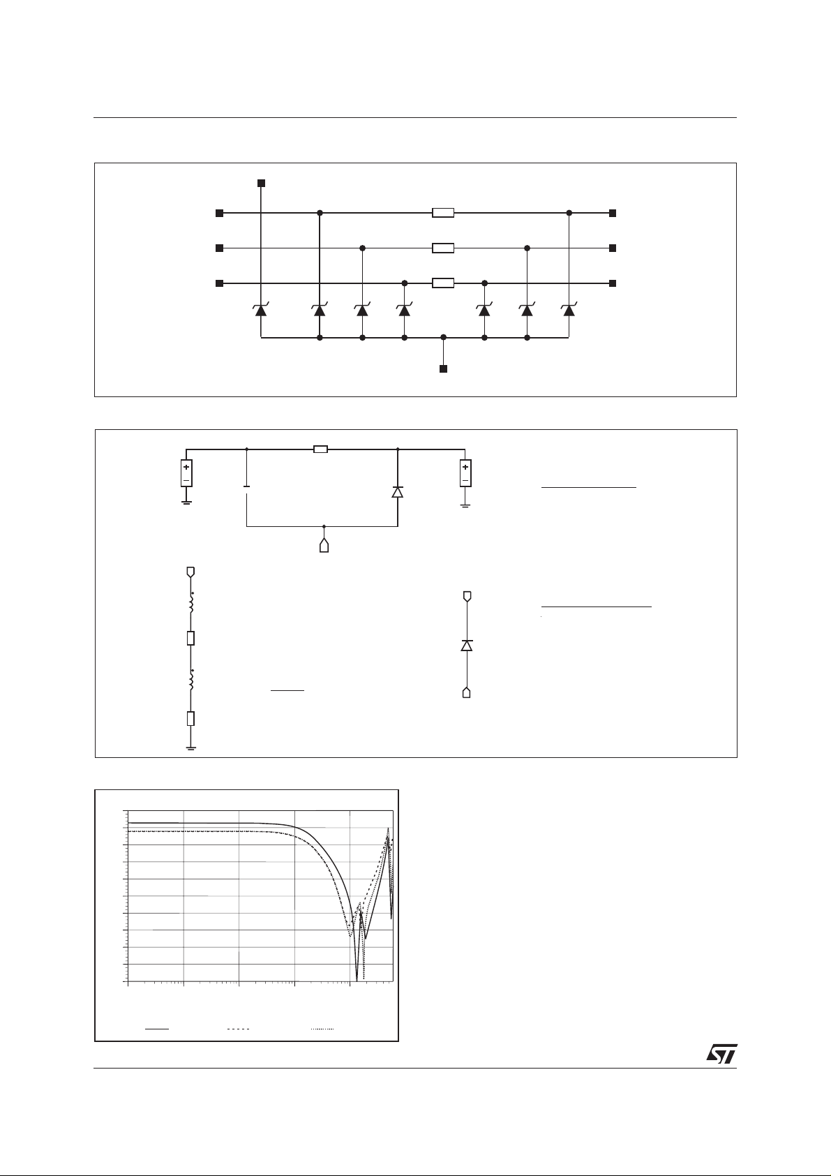
EMIF03-SIM01
Schematic
C2
Aplac model
sub
A3
B3
C3
Port1
50
50p
0.05
0.08nH
0.1
MODEL = demif03
Rseries = 47R (CLK line)
B2 is ground pin
Rseries
MODEL = demif03
sub
= 100R (RST & Data lines)
100R
47R
100R
GND
Port2
50
Vcc
MODEL = demif03_Vcc
sub
A2
B1
C1
DEMIF03 diodes Model
- RS = 1.2
- CJO = 17p
- M = 0.3333
- VJ = 0.6
- ISR = 100p
- BV = 6.8
- IBV = 1m
- TT = 100n
DEMIF03_Vcc diode Model
- RS = 1.5
- CJO = 20p
- M = 0.3333
- VJ = 0.6
- ISR = 100p
- BV = 6.8
- IBV = 1m
- TT = 100n
Filtering behavior
0.00
-5.00
-10.00
-15.00
-20.00
-25.00
-30.00
-35.00
-40.00
-45.00
-50.00
2/11
dB
Aplac 7.60 User: STMicroelectronics Feb 22 2001
100.0k 1.0M 10.0M 100.0M
f/Hz
B3_B1(CLK) A3_A2(RST)
1.0G
C3_C1(DAT)
Page 3
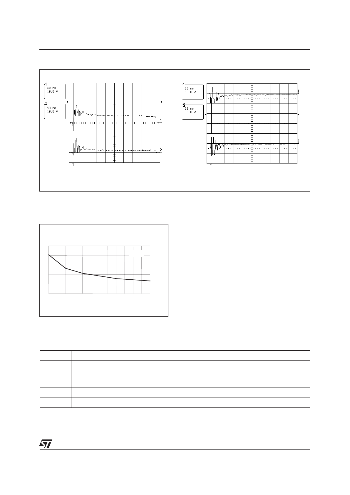
ESD response to IEC61000-4-2 (15kV air discharge)
Positive surge Negative surge
EMIF03-SIM01
Capacitance versus reverse applied voltage.
C(pF)
35
30
25
20
15
10
0123456
ABSOLUTE MAXIMUM RATINGS (T
F=1MHz
Vosc=30mV
amb
VR(V)
=25°C)
Symbol Parameter and test conditions Value Unit
V
PP
ESD discharge IEC61000-4-2, air discharge
ESD discharge IEC61000-4-2, contact discharge
T
j
T
op
T
stg
Junction temperature
Operating temperature range
Storage temperature range
15
8
125 °C
-40 to + 85 °C
-55 to +150 °C
kV
3/11
Page 4
EMIF03-SIM01
ELECTRICAL CHARACTERISTICS (T
amb
=25°C)
Symbol Parameter
V
V
V
I
RM
Rd
I
PP
BR
RM
CL
Breakdown voltage
Leakage current @ V
Stand-off voltage
Clamping voltage
Dynamic impedance
Peak pulse current
RM
Symbol Test conditions Min. Typ. Max. Unit
V
BR
I
RM
R
d
R
1
R
2
R
3
C
line
IR=1mA
VRM=3V
@0V
6V
1 µA
1.5 Ω
95 100 105 Ω
44.65 47 49.35 Ω
95 100 105 Ω
35 pF
TECHNICAL INFORMATION
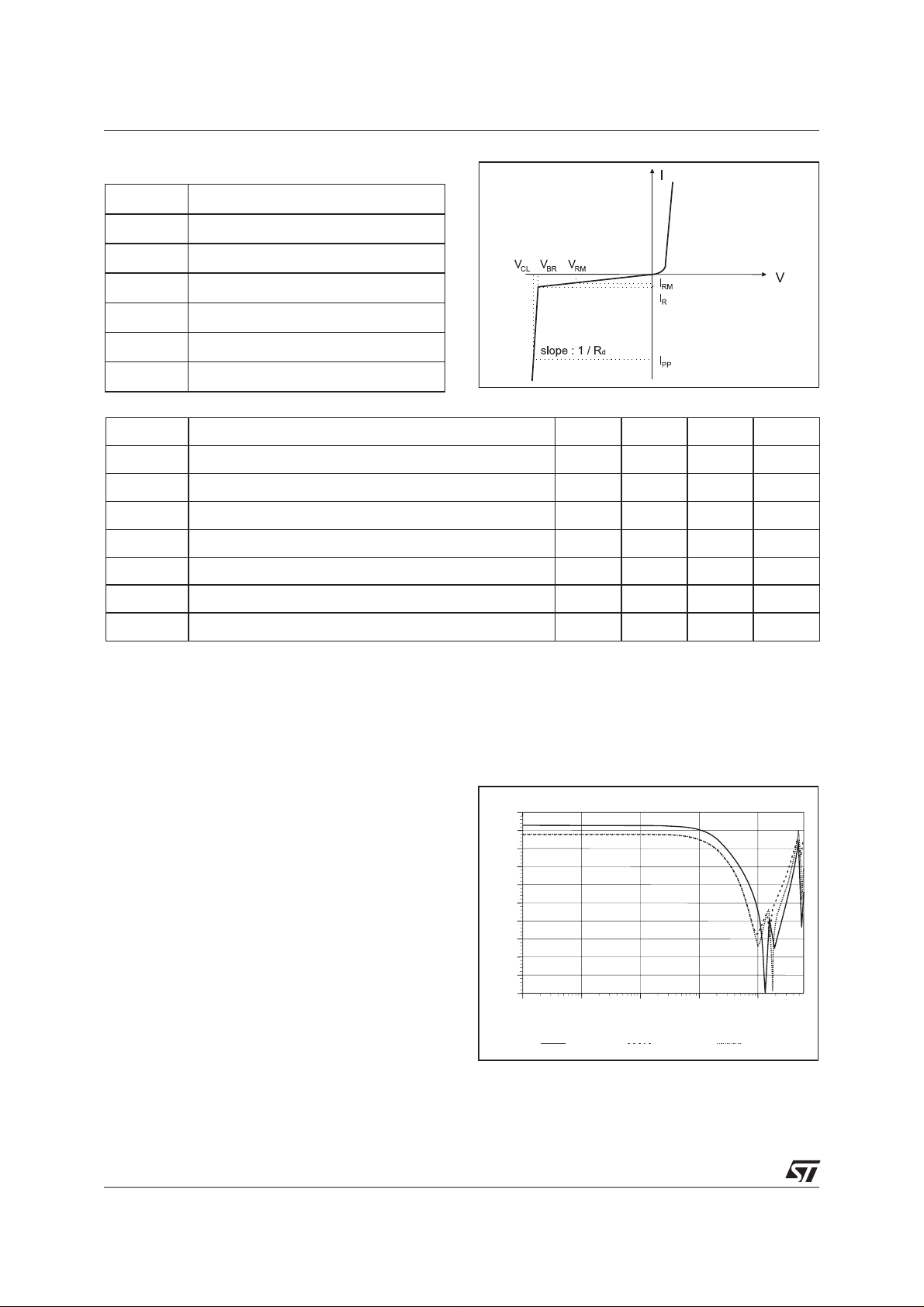
FREQUENCY BEHAVIOR
The EMIF03-SIM01is firstly designed as anEMI
/ RFI filter. This low-pass filter is characterized
by the following parameters:
- Cut-off frequency
- Insertion loss
- High frequency rejection
Figure A1shows that attenuation is better than
-20dB at mobile phone frequencies (800MHz to
2.5GHz).
4/11
Fig. A1: Frequency response curve
0.00
dB
-5.00
-10.00
-15.00
-20.00
-25.00
-30.00
-35.00
-40.00
-45.00
-50.00
Aplac 7.60 User: STMicroelectronics Feb 22 2001
100.0k 1.0M 10.0M 100.0M
f/Hz
B3_B1(CLK) A3_A2(RST)
C3_C1(DAT)
1.0G
Page 5

Fig. A2: Measurements conditions
50 Ω
TEST BOARD
EMI03
SIM01
EMIF03-SIM01
Vg
50 Ω
ESD PROTECTION
In addition with the filtering the EMIF03-SIM01 is particularly optimized to perform ESD protection.
ESD protection is based on the use of device which clamps at:
VVRI
cl br d pp
=+⋅
This protection function is splitted in 2 stages. As shown in Figure A3, the ESD strikes are clamped by the
first stage S1 and then its remaining overvoltage is applied to the second stage through the resistor R.
Such a configuration makes the output voltage very low at the Vout level.
Fig. A3: ESD clamping behavior
Rg
S1
R = 100 or 47ΩΩS2
Rd Rd
Vg
V
BR VBR
Vin
Vout
R load
Device
to be
ESD Surge
protected
EMIF03-SIM01
5/11
Page 6

EMIF03-SIM01
To have a good approximation of the remaining voltages at both Vin and Vout stages, we give the typical
dynamic resistance value Rd. By taking into account these following hypothesis : R>>Rd, Rg>>Rd and
Rload>>Rd, it gives these formulas:
RV RV
gbr dg
Vinput
Voutput
The results of the calculation done for an IEC 1000-4-2 Level 4 Contact Discharge surge (Vg=8kV,
Rg=330Ω ) and Vbr=7V (typ.) give:
Vinput = 43.36V
Voutput = 7.65V (R = 100Ω)
This confirms the verylow remaining voltage across the device to be protected. It is also important to note
that in this approximation the parasitic inductance effect was not taken into account. This could be few
tenths of volts during few ns at theVin side. This parasitic effect is not present at the Voutside due the low
current involved after the series resistance R.
⋅+⋅
=
=
R
g
br d in
RV R V
⋅+⋅
R
8.38V (R = 47Ω)
LATCH-UP PHENOMENA
The early ageing and destruction of IC’s is often due to latch-up phenomena which mainly induced by
dV/dt. Thanks to itsRC structure, theEMIF03-SIM01 provides ahigh immunity tolatch-up by integrationof
fast edges. (Please refer to the response of the EMIF03-SIM01 to a 30 ns edge on Fig. A9)
The measurements done here after show very clearly (Fig. A5a & A5b) the high efficiency of the ESD
protection :
- almost no influence of the parasitic inductances on Vout stage
- Vout clamping voltage very close to Vbr for positive surge and close to ground for negative one
Fig. A4: Measurements conditions
TEST BOARD
V(in) V(out)
EMI03
SIM01
6/11
Page 7

Fig. A5: Remaining voltage at both stages S1 (Vin1) and S2 (Vout1) during ESD surge
EMIF03-SIM01
a: Positive Surge
Please note that the EMIF03-SIM01 is not only acting for positive ESD surges but also for negative ones.
For negatives surges, it clamps close to ground voltage as shown in Fig. A5b.
Note: Dynamic resistance measurements
Fig. A6: Rd measurement current wave
I
As the value of the dynamic resistance remains
stable for a surge duration lower than 20µs, the
2.5µs rectangular surge is well adapted. In
IPP
tt
addition both rise and fall times are optimized to
avoid any parasitic phenomenon during the
measurement of Rd
b: Negative Surge
2µs
2.5 µs
2.5 µs duration measurement wave
7/11
Page 8

CROSSTALK BEHAVIOR
Fig. A7: Crosstalk phenomena
EMIF03-SIM01
RG1
V
G1
RG2
VG2
Line 1
Line 2
R
L1
R
L2
αβ
αβ
V+ V
1G1 12G2
V+ V
2G2 21G1
DRIVERS RECEIVERS
The crosstalk phenomena are due to the coupling between 2 lines. The coupling factor ( β12 or β21 )
increases when the gap across lines decreases, particularly in silicon dice. In the example above the
expected signal on load R
21VG1. Thispart of theVG1 signal represents theeffect of thecrosstalk phenomenon of the line 1 on
β
L2 is α2VG2, in fact the real voltage at this point has got an extra value
the line 2.This phenomenon has to be taken into account when the drivers impose fastdigital data or
high frequency analog signals in the disturbingline. The perturbedline will bemore affected ifit works
with low voltage signal or high load impedance (few kΩ).
1- Digital crosstalk
Fig. A8: Digital crosstalk measurements
+3V
74HC04
Square
+3V
Pulse
Generator
VG1
Square pulse generator
■
frequency = 3.3MHz
■
0 - 3.3V
■
Risetime = 30ns
B1
C1
EMI35
SIM01
+3V
74HC04
B3
®
C3
β21 G1V
8/11
Page 9

Fig. A9: Digital crosstalk results
Digital crosstalk is less than 2 mV peak to peak
EMIF03-SIM01
2- Analog crosstalk
Fig. A10: Analog crosstalk phenomena
TEST BOARD
out1
50 Ω
EMI35
SIM01
50 Ω
in1
Vg
9/11
Page 10

EMIF03-SIM01
Fig. A11: Analog crosstalk results
Aplac 7.60 User: STMicroelectronics Feb 22 2001
0.00
dB
-10.00
-20.00
-30.00
-40.00
-50.00
-60.00
-70.00
-80.00
-90.00
-100.0
100.0k 1.0M 10.0M 100.0M 1.0G
f/Hz
Figure A10 gives the measurement circuit for the analog application. In Figure A11, the curve shows the
EMIF03-SIM01 provides a crosstalk immunity better than - 20dB up to 3GHz.
ORDER CODE
B3_C1
EMIF 03 SIM 01-
Electro Magnetic
Interference Filter
PACKAGE MECHANICAL DATA
(all dimensions in µm)
Version number
Nb of lines
SIM Card protection
500µm ± 50
650µm ± 65
315µm ± 50
1.57mm ± 50µm
1.57mm ± 50µm
■
Bottom side (ball view): Pin A1 missing for die orientation
■
Top side (balls underweath): see the marking .
10/11
Page 11

MARKING and DIE SIZE (typical values)
EMIF03-SIM01
365
365
diam 230
1570
200
FCT
®
220
YWW
1570
YWW: Date code (year + week code)
PACKING
Ordering code Marking Package Weight Base qty Delivery mode
EMIF03-SIM01
FCT Flip Chip 3.3 mg 5000 Tape & reel 7”
Note: More packing information are available in the application note AN1235: “Flip-Chip: Package
description and recommendations for use”
Informationfurnishedisbelievedtobe accurate and reliable. However, STMicroelectronics assumes no responsibility for the consequences of
useofsuch information nor for any infringement of patents or other rights of third parties which may resultfrom its use. No license is granted by
implication or otherwise under any patent or patent rights of STMicroelectronics. Specifications mentioned in this publication are subject to
change without notice. This publication supersedes and replaces all information previously supplied.
STMicroelectronics products are not authorized for use as critical components in life support devices or systems without express written approval of STMicroelectronics.
The ST logo is a registered trademark of STMicroelectronics
© 2002 STMicroelectronics - Printed in Italy - All rights reserved.
STMicroelectronics GROUP OF COMPANIES
Australia - Brazil - Canada - China - Finland - France - Germany
Hong Kong - India - Israel - Italy - Japan - Malaysia - Malta - Morocco - Singapore
Spain - Sweden - Switzerland - United Kingdom - United States.
http://www.st.com
11/11
 Loading...