

Page 1
EMIF02-600FU7
Application Specific Discretes
A.S.D.
MAINAPPLICATIONS
WhereEMIfilteringin ESDsensitive equipment is required :
Computers and printers
Communication systems
Mobile phones
MCU Boards
DESCRIPTION
The EMIF02-600FU7 isa highlyintegrated array designed
to suppress EMI / RFI noise in all systems subjected to
electromagnetic interferences.
Additionally, this filter includes an ESD protectioncircuitry
whichprevents theprotected devicefrom destructionwhen
subjected to ESD surges up to 15 kV. The
EMIF02-600FU7 provides best efficiency when using
separated inputs and outputs, in the so-called 4-points
structure.
BENEFITS
10-bit EMI bi-directionallow-pass-filter
Enhanced ESD protectionfor theprotected device,op-
timized by the four pointstructure
High flexibility in the design of highdensity boards
COMPLIES WITHTHE FOLLOWINGSTANDARDS :
IEC 1000-4-2 15kV (air discharge)
8 kV (contact discharge)
TM
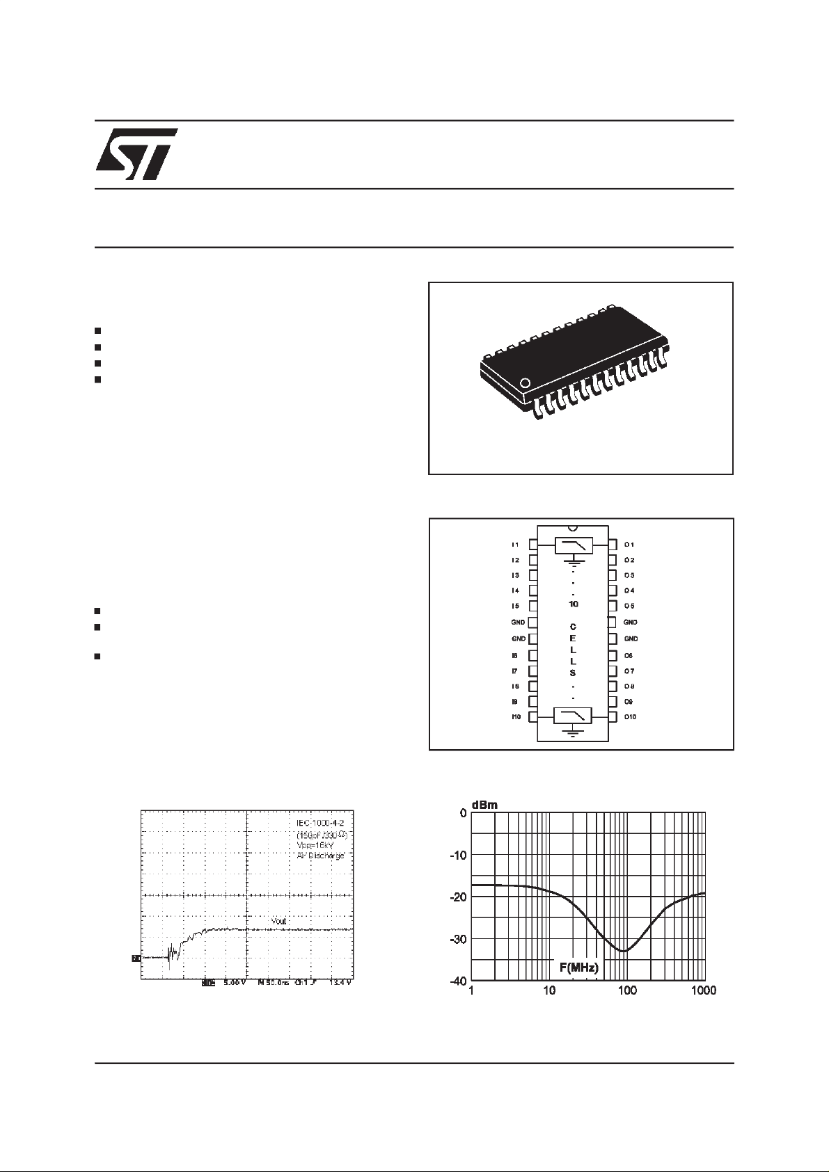
10-BIT WIDE EMI FILTER
INCUDING ESD PROTECTION
SSOP24
FUNCTIONAL DIAGRAM
.
.
.
10
C
E
L
L
S
.
.
.
ESDresponsetoIEC1000-4-2 (15kVairdischarge) Filteringresponse(with 50Ω line)
TM : ASDis trademark of STMicroelectronics.
September 1998 - Ed: 2A
1/9
Page 2
EMIF02-600FU7
ABSOLUTEMAXIMUM RATINGS(T
amb
=25°C)
Symbol Parameterand test conditions Value Unit
V
PP
ESDdischargeIEC1000-4-2,air discharge
ESDdischargeIEC1000-4-2,contactdischarge
T
j
T
op
T
stg
T
L
Junctiontemperature 150 °C
Operatingtemperaturerange
Storagetemperature range -55to +150 °C
Leadsolder temperature(10 secondduration) 260 °C
ELECTRICALCHARACTE RISTICS (T
amb
=25 °C)
16
9
-40 to+ 85 °C
Symbol Parameter
V
BR
I
RM
V
RM
V
CL
Breakdownvoltage
Leakagecurrent @ V
Stand-offvoltage
Clampingvoltage
RM
Rd Dynamicimpedance
I
PP
Peak pulsecurrent
kV
R
I/O
Serialresistancebetween Input
and Output
Symbol Testconditions Min. Typ. Max. Unit
V
BR
I
RM
R
I/O
R
d
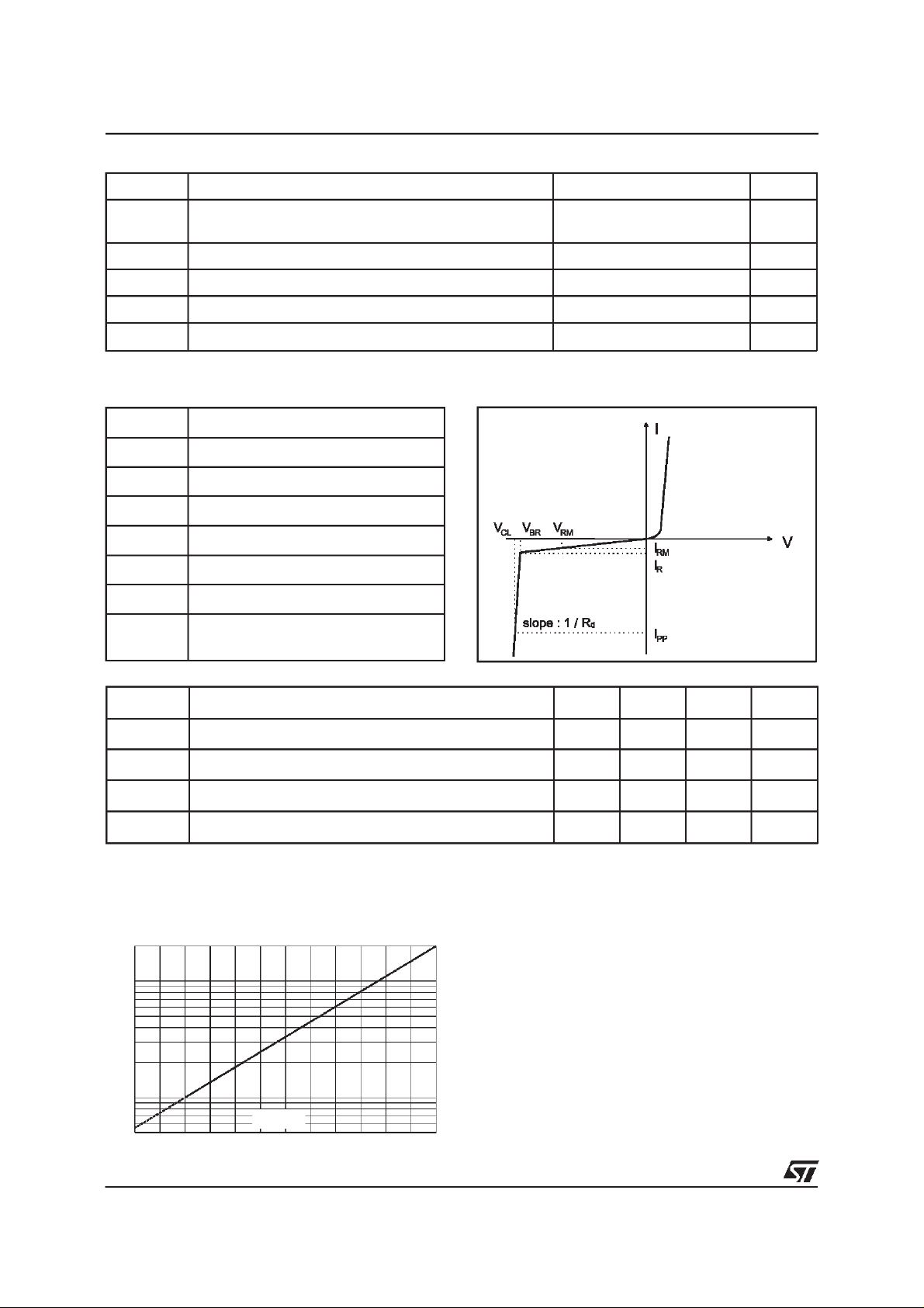
Note 1 : to calculatethe ESDresidual voltage, please refer to the paragraph ”ESDPROTECTION” on pages4 & 5
IR=1mA 6 7 8 V
VRM=3V 1 µA
Serialresistancebetween Inputand Output 480 600 720 Ω
Ipp=10A,tp=2.5µs (see note1) 0.55 Ω
Fig.1: Relativevariationof leakagecurrentversus
reversevoltage(Typicalvalues)
IR[VR] / IR[VR=3V]
20.0
10.0
5.0
2.0
1.0
0.5
2.5 3.0 3.5 4.0 4.5 5.0 5.5
2/9
VR (V)
Page 3
EMIF02-600FU7
TECHNICAL INFORMATION
FREQUENCY BEHAVIOR
The EMIF02-600FU7 is firstly designed as an EMI/RFI filter. This low-pass filter is characterized by the following
parameters:
- Cut-off frequency
- Insertionloss
- High frequency rejection
FigA1: EMIF02- 600F U 7frequencyresponsecurve.
Figure A1gives these parameters, in particularthe signal rejection at theGSM frequency is about -20dBm at 900MHz,
while theattenuation for FM broadcast range(around 100MHz) is better than -32dBm
FigA2 : Measurementconditions
SPECTRUM
VoutVin
ANALYSER
50
Ω
TG OUTPUT
TEST BOARD
EMIF02
RF INPUT
Vg
50
Ω
EMIF02
3/9
Page 4

EMIF02-600FU7
ESDPROTECTION
In additionto its filtering function, the EMIF02-600FU7 is particularly optimized to perform ESD protection.
ESD protection is based onvoltage clampingwhich can be calculated by :
VCL=VBR+Rd.I
PP
This protection function is splittedin 2stages. Asshown infigure A3,the ESDstrikes areclamped by the first stageS1 and
then its remainingovervoltage is applied to the secondstage through the resistorR. Sucha configurationmakes the output
voltage V
very low.
out
FigA3 : ESDclamping behavior
Rg
ESD
Surge
Vg
Vin
Rd
Vbr
S1
To have a good approximation of the remaining voltages at both Vin and Vout stages, we provide the typical dynamical
resistance value Rd. By takinginto accountthese following hypothesis : R>>Rd, R
formulas:
Vin
=
Vout
R
EMIF02-600FU7
Rg.Vbr+Rd.Vg
Rg
R.Vbr+Rd.Vin
=
R
S2
Rd
Vbr
Vout
Device to be protected
>>Rd and Rload>>Rd, it gives these
G
Rload
The results of the calculation done forVG=8kV, RG=330Ω(IEC1000-4-2 standard) and VBR=7V (typ.)give:
Vin = 20.33V
Vout = 7.01 V
This confirms the very low remaining voltage across the device to be protected. It is also important to note that in this
approximation theparasitic inductance effect was not takeninto account. This could be few tenthsof volts during few ns at
the Vin side.This parasitic effect is notpresent at theVout side due the low current involved after the resistance R.
The measurements shown here after illustrate very clearly (Fig. A5a) the high efficiency of the ESDprotection :
- no influence of the parasitic inductanceson Vout stage
- Vout clamping voltage very close to V
BR
FigA4 : Measurementconditions
LOW-PASS FILTER
Vin Vout
GND
GND
GND
4/9
Page 5

EMIF02-600FU7
Fig A5: Remainingvoltageat bothstagesS1 (Vin)and S2 (Vout)during ESDsurge
a) Positivesurge b) Negativesurge
Please note that the EMIF02-600FU7 is not only acting for positive ESD surgesbut also for negative ones. For these kind
of disturbancesit clamps close to ground voltageas shown in Fig. A5b.
NOTE: DYNAMIC RESISTANCE MEASUREMENT
As thevalue ofthe dynamic resistance remainsstable for a
surge durationlower than 20µs,the 2.5µsrectangularsurge
is well adapted. In addition both rise and fall times are
optimized to avoid any parasitic phenomenon during the
measurement of Rd.
CROSSTALK BEHAVIOR
1- Crosstalkphenomena
FigA7 : Crosstalkphenomena
R
G1
V
G1
V
G2
R
G2
line 1
line 2
FigA6 : Rd measurementcurrentwave
I
I
PP
2 µs
2.5 µs
2.5µs duration measurement wave
R
L1
R
L2
α
V
G2
β
α
V
β
G1
V
G2
V
G1
tt
DRIVERS RECEIVERS
The crosstalk phenomena are due to the coupling between 2 lines. The coupling factor ( β12or β21) increases when the
gap across lines decreases, particularlyin silicondice. In the exampleabove the expected signal on load R
fact the real voltage at this point has got an extra valueβ21V
. This part of the VG1signal represents the effect of the
G1
isα2VG2,in
L2
crosstalk phenomenon of the line 1 on the line 2. This phenomenonhas to be taken into account whenthe drivers impose
fast digital data or high frequency analog signals in the disturbing line. The perturbed line will be more affected if it works
with low voltage signal or high load impedance (few kΩ). The following chapters give the value of both digital and analog
crosstalk.
5/9
Page 6

EMIF02-600FU7
2- DigitalCrosstalk
FigA8 : Digitalcrosstalkmeasurement
+5V +5V
74HC04 74HC04
Line 1
V
Square
Pulse
Generator
5KHz
+5V
Figure A8shows themeasurement circuit used toquantifythe crosstalk effect in a classicaldigital application.
Figure A9shows that in sucha conditionsignal from 0 to 5V and risetime of10 ns, the impact on thedisturbed line isless
than20mV peaktopeak. No datadisturbance was notedon the concernedline. Thesame results were obtained withfalling
edges.
FigA9 : Digitalcrosstalkresults
G1
Line 2
β
V
G1
21
3- AnalogCrosstalk
Fig A10 : Analogcrosstalkmeasurement
FigA11 : Typicalanalog crosstalkresult
dB
0
-10
-20
TG OUTPUT RF INPUT
-30
-40
TEST BOARD
-50
-60
EMIF02
Figure A10 gives themeasurement circuit for the analog application. In figure A11, the curveshows the effectof cell 1/24
on cell 2/23, no difference was foundwith othercouples of adjacentcells. In usual frequency range of analog signals (up to
100MHz) the effect on disturbed line is lessthan -32 dBm.
6/9
-70
-80
1 10 100
F(MHz)
Page 7

PSPICEMODEL
FigA12: PSpicemodelofoneEMIF02-600F U 7cell
EMIF02-600FU7
5nH 5nH
Input Output
Dzin
1
Ω
FigureA12 shows thePSpice model of one cell ofthe EMIF02-600FU7.In thismodel, theclampingdiodes (Dzin andDzout)
are definedby the following PSpice parameters :
RS = 0.55
Cjo =100p
M = 0.3333
VJ = 0.6
BV =7
IBV = 1u
This model isavailable for frequencysimulation and for ambient temperature of 27°C.
The comparison betweenthe PSpicesimulation andthe measured frequency responseis given in figáA13. Thisshows that
the PSpice model is very close to the product behavior.
600
GND
Ω
0.85nH
1
Ω
Dzout
FigA13 : Comparison betweenPSpice simulation andmeasured frequencyresponse
dBm
0
PSpice
Model
-10
Measured
(smooth)
-20
-30
F(MHz)
-40
1 10 100 1000
7/9
Page 8

EMIF02-600FU7
PACKAGEMECHANICAL DATA
SSOP24
b
D
L
A
e
S
a1
b1
E
24
1
13
12
DIMENSIONS
REF.
Millimeters Inches
Min. Typ. Max. Min. Typ. Max.
A 1.73 1.86 2.00 0.068 0.073 0.079
a1 0.05 0.25 0.002 0.010
b 0.25 0.35 0.010 0.014
b1 0.10 0.35 0.0035 0.014
D 8.07 8.20 8.33 0.317 0.322 0.328
E 7.60 7.90 0.299 0.311
e 0.65 0.0256
F 5.20 5.38 0.2047 0.2118
L 0.25 0.88 0.010 0.0347
S8°max
F
Mechanicalspecifications
Lead plating Tin-lead
Lead platingthickness 7µmmin.
20 µmmax.
Lead material Copper alloy
Lead coplanarity 0.08mmmax.
Body material Moldedepoxy
Flammability UL94V-0
RECOMMENDED FOOTPRINT
0.65mm
8.3mm 5.3mm
8/9
0.45mm
Page 9

ORDERCODE
EMIF02-600FU7
EMIF 02
ELECTROMAGNETIC
INTERFERENCEFILTER
600 F U 7 RL
-
R
value
I/O
RL : Tape& Reel
SSOP24package
NUMERICALCODE
Unidirectional transildiode
Four pointstructure
Ordercode Marking Package Weight Base qty
Delivery
mode
EMIF02-600FU7 EMIF02-600 SSOP24 0.19g 59 tube
EMIF02-600FU7RL EMIF02-600 SSOP24 0.19g 2000 tape & reel
Informationfurnishedis believed to beaccurate andreliable. However, STMicroelectronics assumes no responsibility for theconsequences of
use of such informationnor for any infringementof patentsor otherrights of third parties which may resultfrom its use.No licenseis granted by
implication or otherwise under any patent or patent rights of STMicroelectronics. Specifications mentioned in this publication are subject to
change without notice. This publicationsupersedes and replaces all informationpreviously supplied.
STMicroelectronics products are not authorized for use as criticalcomponents in life support devices or systems withoutexpress writtenapproval of STMicroelectronics.
The ST logois a registeredtrademark of STMicroelectronics
1998 STMicroelectronics - Printed inItaly - All rights reserved.
STMicroelectronics GROUP OF COMPANIES
Australia - Brazil - Canada - China - France - Germany - Italy - Japan - Korea - Malaysia - Malta - Mexico - Morocco -
The Netherlands - Singapore - Spain - Sweden - Switzerland - Taiwan - Thailand - United Kingdom - U.S.A.
http://www.st.com
9/9
 Loading...