

Page 1
GENERAL DESCRIPTION
The EM91215 is a series of tone/pulse switchable dialers that is composed of T/P dialer and T/P dialer with 13
set memories. The EM91215 series provides necessary functions of telephone set for application in any
environment, such as Pulse dialing, Tone (DTMF) dialing, Handfree dialing, keying tone , mute and pulse mute
functions. Beside this, SDO (Serial Data Output) functions is provided in advance version that is designed to
drive LCD driver and voice synthesizer. In this application, the dialing numbers can be displayed on LCD screen
with EM32100 ( or EM32116 ).
FEATURES
•Tone/Pulse switchable.
• Wide operating voltage from 2.0 V to 5.5 V.
•Low operating current, 0.15 mA (Pulse) and 0.3 mA (Tone) typically.
•Adding resistor on keyboard scan pin that can select many telephone specifications, such as : Pulse rate,
M/B ratio, Flash time, Pause time, P-T wait time and keyboard type.
•SDO function supports LCD driver and voice synthesizer to indicate dialing numbers.
•Handfree function provides on-hook dialing and speakerphone application.
•13 set one touch or (3 set one touch and 10 set two touch) repertory memory, each one can store data up to
16 digits.
•A 32-digit LNB (last number) redial memory.
•A 32-digit SAVE redial memory.
•Keytone function provides rapidly keying recognition.
•Pulse mute function supports pulse dialing application.
•Using 3.579545 MHz crystal or ceramic resonator.
•Package forms: PDIP , skinny.
EM91215 SERIES
TONE/PULSE SWITCHABLE DIALER WITH LCD INTERFACE
TONE/PULSE SWITCHABLE DIALER WITH LCD INTERFACE
EM91215 SERIES
ORDERING INFORMATION
Versions list
VERSION LNB KT SAVE HF SDO(LCD) PMUTE
EM91215A √√√ √
EM91215B √√√ √ √
EM91215C √√√ √ √ √
* This specification are subject to be changed without notice.
10.1.1997
1
Page 2
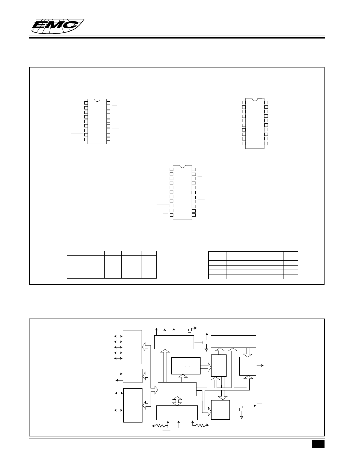
EM91215
Pin Assignment
EM91215 SERIES
TONE/PULSE SWITCHABLE DIALER WITH LCD INTERFACE
EM91215AP
COL5
COL4/KT
COL3
COL2
COL1
XIN
XOUT
XMUTE
VSS
1
2
3
4
5
6
7
8
9
PM
17
PO
16
ROW4
15
ROW3
14
ROW2
13
ROW1
12
HKS
11
VDD
10
DTMF
18
EM91215CK
ROW6
COL5
COL4/KT
COL3
COL2
COL1
XIN
XOUT
XMUTE
VSS
HFI
22
1
21
2
20
3
19
4
18
5
17
6
16
7
15
8
14
9
13
10
12
11
Keyboard Arrangement
Type A Type B
M4
M9
COL5
EM1
EM2
F
EM3
A
ST
M5
M10
ROW5/SDO
ROW1
ROW2
ROW3
ROW4
ROW5/SDO
ROW6
COL1
1
4
7
*/T
M1
M6
COL2
2
5
8
0
M2
M7
COL3
3
6
9
#
M3
M8
COL4/KT
SAVE
RD/P
ROW5/SDO
PM
PO
ROW4
ROW3
ROW2
ROW1
HKS
VDD
DTMF
HFO
ROW1
ROW2
ROW3
ROW4
ROW6
COL1
1
4
7
*
M1
M6
EM91215BP
COL5
COL4/KT
COL3
COL2
COL1
XIN
XOUT
XMUTE
VSS
HFI
COL2
2
5
8
0
M2
M7
20
1
2
3
4
5
6
7
8
9
10
COL3
M3
M8
PM
19
PO
18
ROW4
17
ROW3
16
ROW2
15
ROW1
14
HKS
13
VDD
12
DTMF
11
HFO
M4
M9
COL5
EM1
EM2
F
EM3
A
ST
M5
M10
COL4/KT
P→T
3
6
9
RD/P
#
@When ROW5 is selected by R option (COL5), there are 13 sets one touch memory version in EM91215C
provided.
FUNCTIONAL BLOCK DIAGRAM
HFO
SDO
COL1
COL2
COL3
COL4/KT
COL5
XIN
XOUT
ROW1
ROW6
Keyboard
interface
(column)
Oscillator
Keyboard
~
interface
(Row)
VDD
* This specification are subject to be changed without notice.
PM
Output circuit
Memory
(Melody)
Timing/Control circuit
Input circuit
HKS HFI
XMUTE
latch
decoder
generator
VDD
Row/Column
programming counter
&
D/A
converter
Pulse
DTMF
PO
10.1.1997
2
Page 3
EM91215 SERIES
TONE/PULSE SWITCHABLE DIALER WITH LCD INTERFACE
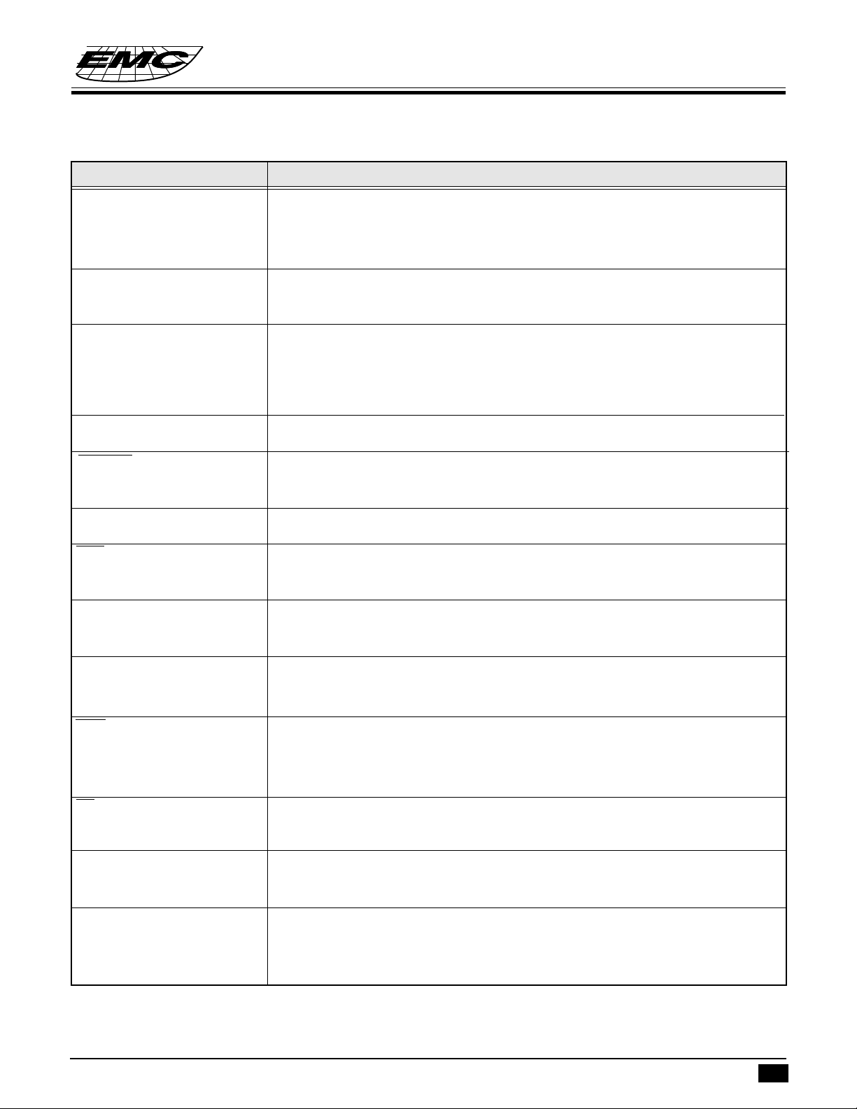
PIN DESCRIPTIONS
Symbol Function
ROW1~ROW6 Keyboard scan pins of row group. In idle state (HKS is “High” and HFO is “Low”),
these pins stay “High impedance” level to prevent power consumption. Otherwise,
these pins switch to “High” level for detecting keyboard entry. These pins will output
600 Hz signal while keyboard is scanning.
COL1~COL3 and COL5 Keyboard scan pins of column group. In idle state, these pins stay “High impedance”
level. Otherwise these pins switch to “Low” level for detecting keyboard entry. These
pins will output 600 Hz signal while keyboard is scanning.
COL4/KT The fourth column group pin of the keyboard that also provides the keytone output
. Normally, this pin stays “Low” level for detecting keyboard entry. After a valid
keyboard entry, this pin will output keying confirmation tone that is 600 Hz signal and
30 ms duration. While DTMF output, the key tone will be disabled. To prevent signal
interference, while DTMF issue, it will disable key tone output except function key.
XIN and XOUT Oscillator input and output pins. A 3.579545 MHz crystal or ceramic resonator must
be crossed connection to XIN and XOUT pins which generate system clock.
XMUTE The Tone/Pulse MUTE signal output pin that is NMOS open-drain output structure.
This pin will switch to “Low” level during Tone/Pulse dialing.
Otherwise, this pin stays “High impedance” level.
V
and V
DD
SS
HFI Handfree inputs pin which accepts falling edge signal to turn “on” or turn “off”
HFO Handfree outputs pin that is designed to control telephone line for on-hook dialing or
DTMF The DTMF (Dual Tone Multi-Frequency) output pin. Normally, this pin stays“Low”
HKS Control signal inputs pin that is corresponding hook switch status. When handset was
PO Pulse signal outputs pin that is NMOS open-drain output structure. Normally, this pin
PM Pulse signal outputs pin that is CMOS inverter output structure. Normally, this pin
SDO SDO function output that is NMOS open-drain structure. When there is a valid entry
Positive and negative power supply input pins. Recommended operating voltage from
2.0Vdc to 5.5Vdc.
handfree function. This pin is hysteresis input structure and built-in pull up resistor
(typically 200 Kohms).
control speakerphone circuit for handfree conversation. When handfree function is
executed, this pin will switch to“High”. Otherwise, this pin stays “Low” level.
level. In Tone dialing mode, this pin will output DTMF signal that is corresponding
to keyboard 0..9, * and # keys.
left from cradle, this pin must be connected to “Low” level to operate all functions.
Otherwise, this pin must be connected to “High” level to disable all function and
prevent power consumption.
stays “High impedance” level. In Pulse dialing mode and keypad was entry. This pin
will output pulse trains signal that is corresponding to keyboard 0 .. 9 keys.
stays “Low” level. During pulse signal dialing or flash function executing, this pin will
switch to “High” level to control the external circuit.
on keyboard, this pin will output a serial data. This serial data is designed to drive LCD
driver to display dialing number on LCD screen or drive voice synthesizer to announce
dialing number to speaker.
* This specification are subject to be changed without notice.
10.1.1997
3
Page 4
FUNCTION DESCRIPTIONS
Dialing signal selection
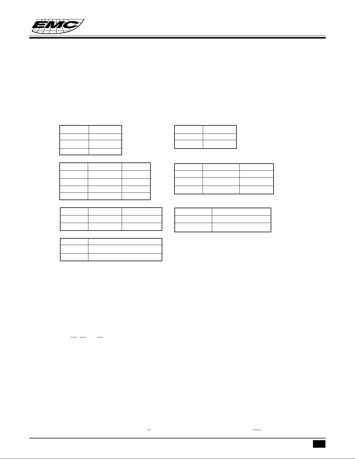
The EM91215 series incorporated a special keyboard scanning function that is connecting a resistor (typically
is 560 Kohms) on keyboard scan pin to select many telephone specifications. The specifications are described
as following :
a. Mode b. M/B ratio
ROW1 Mode ROW2 MBR (%)
R-Vdd 20 PPS NR 40:60
NR Tone R-Vss 33:66
R-Vss 10 PPS
c. Flash time d. DTMF signal
ROW3 ROW4 Tf (ms) COL1 Td (ms) Titp (ms)
NR NR 600 R-Vdd 90 90
NR R-Vss 100 NR 98 98
R-Vss NR 80 R-Vss 83 83
R-Vss R-Vss 300
e. Pause time and P-T wait time f. Keyboard operate type
COL2 Tp (sec) Tpt (ms) COL3 Type
NR 3.6 3.6 NR A
R-Vss 2.0 2.0 R-Vss B
g. ROW5/SDO pin functions
COL5 ROW5/SDO pin
NR SDO
R-Vss ROW5
EM91215 SERIES
TONE/PULSE SWITCHABLE DIALER WITH LCD INTERFACE
(Note): The option of COL5 pin is only for EM91215.
If select SDO function, the memory type is
(1T*3+2T*10)
If select ROW5 function, the memory type is
(1T*3+2T*10) and (1T*13)
Normal dialing
Directly keying digital key on keyboard which number can be dialing output and stored in LNB memory
automatically. Operating procedure described as follow :
• To select Pulse or Tone mode.
• Off-hook or turn on HF function.
• Keying d1, d2, .. , dn. The “d” expressed digital keypad that included 1~9, *, 0, #, P, and P→T keys. The “n”
expressed unlimited.
• The numbers d1, d2, .. , dn will be dialed out in Pulse or Tone mode as selection.
LNB redial memory
Storing:
In normal dialing mode, every digital key was entry which number will be stored in LNB memory
automatically. If entry digits are more than 32 digits, the redial function of LNB memory will be disabled.
Otherwise, these numbers stored in LNB memory can be redial output.
Redialing:
After normal dialing, directly keying
numbers that are stored into LNB memory will be dialed output.
* This specification are subject to be changed without notice.
F key (or On-Off hook once) and keying RD key on keyboard. The
10.1.1997
4
Page 5
EM91215 SERIES
TONE/PULSE SWITCHABLE DIALER WITH LCD INTERFACE
SAVE redial memory
The SAVE meomry is designed in EM91215 series to support 32 digits capacity buffer for second redial,
pager, Memory and other system applications.
Storing : EM91215 series support two operating methods to store numbers into SAVE redial memory.
Method 1
• To select Pulse or Tone mode.
• Off-hook (or turn on HF function), push
d1, d2, .. , dn. The numbers d1, d2, .. , dn will be dialed out in Pulse
or Tone mode as selection.
• After dn had been dialed out and push
[ST], Save key. If the keying numbers are more than 32 digits that
content of SAVE memory can not be updated. Otherwise, these numbers will be stored into SAVE memory.
In the [] key allows to be omitted.
Method 2
Off-hook (or turn on HF function), push ST, d1, d2, .. , dn, [ST], Save. If the keying numbers are not over 32
digits, the numbers d1, d2, .. , dn will be stored in SAVE redial memory automatically.
Dialing :
• To select Pulse or Tone mode.
• Off-hook (or turn on HF function), push Save key. The numbers stored in SAVE memory will be dialed out
in Pulse or Tone mode as selection.
Repertory memory
The EM91215 series incorporated several sets repertory memory and each one can store number up to 16 digits.
These memories were designed to 13 sets types. As operating precedure, all of the memories can be separated
to dirtect (one-touch) and indirect (two-touch ) operation. In memory storing, if stored numbers are more than
16 digits that only the previous 16 digits can be stored into specific memory. Otherwise, these numbers can be
stored entirely. After memory dialed out, the content of LNB is keeping to current data.
Storing of 13 sets memory types
Direct (one-touch) operation
Off-hook (or turn on HF function), push
numbers d1, d2, .. , dn will be stored into memory location “EMn”. The “EMn” expressed emergency memory
EM1 to EM3.
Indirect (two-touch) operation
Off-hook (or turn on HF function), push ST, d1, d2, .. , dn, ST, n. The numbers d1, d2, .. , dn will be stored
into memory location “n”. The “n” expressed digital key from 0 to 9.
ST, d1, d2, .. , dn [ST], EMn or M1~M10 (ROW5 optioned). The
Dialing (after memory dialed out, the content of LNB is keeping to current data)
Direct (one-touch) memory operation
• To select Pulse or Tone mode.
• Off-hook (or Turn on HF function), push
Mn (or EMn) key. The numbers that are stored in direct memory
location “Mn (or EMn)” will be dialed out in Pulse or Tone mode as selection. The “n” expressed digital
* This specification are subject to be changed without notice.
10.1.1997
5
Page 6
EM91215 SERIES
TONE/PULSE SWITCHABLE DIALER WITH LCD INTERFACE
number from 1~10 decided by dialers’ memory sets.
Indirect (two-touch) memory
• To select Pulse or Tone mode.
• Off-hook (or Turn on HF function), push A, n key. The numbers that are stored in indirect memory location
“n” will be dialed out in Pulse or Tone mode as selection. The “n” expressed digital key from 0 to 9.
Pause (P) key operation
The Pause (P) key is designed to support pause operation in dialing duration. “P” key can be stored in memory
and it will occupy one digital position.
• To select Pulse or Tone mode.
• Off-hook (or turn on HF function), push
out as following sequence:
d1, d2, .. , dn, Tp, k1, k2, .. , kn.
d1, d2, .. , dn, RD/P, k1, k2, .. , kn . These numbers will be dialed
Pulse to Tone (*/T or P-T) key operation
The Pulse to Tone (*/T or P-T) key is designed to support toll dialing (long distance call) or PABX system
operation. The "*/T (or P-T)" key can be stored in memory and it will occupy one digital position.
• To select Pulse mode.
• Off-hook (or turn on HF function), push d1, d2, .. , dn, */T, (or P-T) k1, k2, .. , kn. These numbers will be dialed
out as following sequence:
d1, d2, .. , dn, Tpt, k1, k2, .. , kn.
(pulse mode) (tone mode)
Flash (F) key operation
The Flash (F) key is designed to break telephone line temporarily. After F key is depressed, this dialer will send
a flash signal to break line 600 ms, 300 ms, 100 ms or 80 ms as ROW3 and ROW4 selection.
Handfree (HF) function
The handfree function is designed to support on-hook dialing and loudspeaker application which can be turn “on”
or “off” with falling edge signal from HFI pin. During handfree function is executed, the HFO pin is switched
to “high”. Otherwise the HFO pin stays “low” level.
Truth table
Operating state Input/Output pin level
HKS PO XMUTE PM HFO
(0) On-hook, idle state H F F L L
(1) Off-hook line L F F L L
(2) Off-hook, HF line L F F L H
(3) On-hook, HF line H F F L H
Note : F=floating (high impedance); H=logic “High”; L=logic “Low” level.
* This specification are subject to be changed without notice.
10.1.1997
6
Page 7

EM91215 SERIES
TONE/PULSE SWITCHABLE DIALER WITH LCD INTERFACE
SDO (Serial Data Output) function
The SDO is serial data output which format is same as UART protocol. SDO function is designed to drive LCD
driver and voice synthesizer. So the dialing numbers can be display on LCD screen with EM32100 (or EM32116
). The SDO signal consists of two start bits, six data bits and two stop bits. Each bit time is about 3.9 ms (256 Hz)
and output sequences are following by start bits, data bits (LSB to MSB) and stop bits.
1
stop bits
ready
0
start bits
1 bit 0
bit1
bit2 bit3 bit4 bit5
data bits
0
SDO Keypad Encoded table:
♦ Digital key (b5,b4=0,0)
keypad 1 2 3 4 56789 0“*”/T # P */”T” or P- T
output
b3,b2,b1,b0 0001 0010 0011 0100 0101 0110 0111 1000 1001 1010 1011 1100 1101 1110
Display 1 2 3 4 56789 0P
♦ Function key (b5,b4=1,0)
keypad F
output
b3,b2,b1,b0 1111
Display clear all display
∗ Keypad,SDO format and LCD display reference table:
Keypad bit5 bit4 bit3 bit2 bit1 bit0 Display
1000001 1
2000010 2
3000011 3
4000100 4
5000101 5
6000110 6
7000111 7
8001000 8
9001001 9
0001010 0
“*”/T 0 0 1 0 1 1
#001100
P001101 P
*/”T” or P-T 0 0 1 1 1 0
F 1 0 1 1 1 1 clear all display
* This specification are subject to be changed without notice.
10.1.1997
7
Page 8

EM91215 SERIES
TONE/PULSE SWITCHABLE DIALER WITH LCD INTERFACE
ABSOLUTE MAXIMUM RATINGS(Ambient temperature is 25 °C, all voltages referenced to V
)
SS
Items Sym. Rating Unit
Power supply voltage V
Input voltage range V
Operating temperature T
Storage temperature T
Power consumption P
DD
IN
OPR
STO
D
VSS-0.3V ~ VDD+0.3V V
6.0 Vdc V
0 ~ +50 °C
-55 ~ 125 °C
500 mW
ELECTRICAL CHARACTERISTICS
(Ambient temperature is 25 °C, VDD=2.5V unless otherwise noted, all voltages referenced to VSS, Fosc=3.579545 MHz)
Parameter Sym. Min. Typ. Max. Unit Condition
Operating voltage Pulse 2.0 - 5.5 V unload
Tone 2.0 - 5.5
Operating current(HKS=0) Pulse Idd - 0.15 0.3 unload
Tone - 0.3 0.5 mA
Pulse - 0.15 0.3 with pull up/down
Tone - 0.3 0.5 resistor * 8
Memory retention current Imrt - 0.001 0.1 uA HKS=1,Vdd=1V
Standby current HKS=1 Istby - 0.001 0.1 unload
HKS=0 - 1 10 uA
HKS=1 -0.001 0.1 with pull up/down
HKS=0 - 10 30 resistor * 8
HKS, HFI ViH 0.8Vdd - Vdd V
pins: input voltage ViL Vss - 0.2Vdd
HFO & PM pins source current IoH 0.2 - - mA Vo = 2.0 V
PO, HFO, XMUTE, IoL -0.2 - - mA Vo = 0.5 V
& PM, SDO pins: sink current
PO, XMUTE and SDO IoH - - ±0.001 uA Vo = Vdd
pins: leakage current
HFI pin input resistance Rhfi - 200 - KΩ Vhfi = Vss
Keyboard scanning pins IoH 2 10 50 uA Vksn=Vss
output current (except COL4/KT) IoL 200 400 800 Vksn=Vdd
COL4/KT source current IoH 0.2 - - mA Vo=2.0V
sink current IoL 0.2 - - Vo=0.5V
* This specification are subject to be changed without notice.
10.1.1997
8
Page 9

EM91215 SERIES
TONE/PULSE SWITCHABLE DIALER WITH LCD INTERFACE
ELECTRICAL CHARACTERISTIC
(Ambient temperature is 25°C, V
Parameter Sym. Min. Typ. Max. Unit Condition
Keyboard debounce time Tdb - 20 - ms
Key tone signal:
frequency Fkt - 600 - Hz
○○○○○○○○○○○○○○○○○○○
present duration Tkt - 30 - ms
Pause time and pulse to tone Tp - 3.6 - sec. COL2=NR
Flash time Tf - 600 - Row3, Row4=NR, NR
Flash pause time Tfp - 300 - ms
Pulse rate PSR - 20 - pps Row1 = R-Vdd
Make/Break ratio MBR - 40:60 - % Row2 = NR
Inter-digit pause time Tidp - 800 - ms PSR = 10 pps
DTMF pin: sink current IoL -0.2 - - mA Vdtmf = 0.5 V
DTMF signal DC level Vdc 0.5 - 0.75 Vdd Vdd = 2.0V ~ 5.5V
DTMF signal: ac level Vdtmf 142 160 180 mVrms Row group
○○○○○○○○○○○○○○○○○○○
pre-emphase Twist 1 2 3 dB Column - Row
○○○○○○○○○○○○○○○○○○○
distortion THD - -30 -23 dB RL = 5 KΩ
○○○○○○○○○○○○○○○○○○○
load resistance ZL 5 - - KΩ THD <−23dB
Minimum tone duration T
Minimum inter-tone pause Titp 88 90 92 ms Memory dialing
SDO every bit time Tbit 3.8 3.9 4.1 ms
=2.5V unless otherwise noted, all voltages referenced to Vss,Fosc=3.579545 MHz)
DD
Tpt - 2 - sec. COL2=R-Vss
- 100 - ms Row3, Row4=NR, R-Vss
- 80 - Row3, Row4=R-Vss, NR
- 300 - Row3, Row4=R-Vss,R-Vss
- 10 - Row1 = R-Vss
- 33:66 - Row2 = R-Vss
- 500 - PSR = 20 pps
96 98 100
D
88 90 92 ms Memory dialing
81 83 85
96 98 100
81 83 85
DTMF output frequency (fosc = 3.579545 MHz)
Keyboard scan pin CCITT standard (Hz) Actual output (Hz) Deviation (%)
ROW1 (f1) 697 699.1 0.30
ROW2 (f2) 770 766.2 0.49
ROW3 (f3) 852 847.4 -0.53
ROW4 (f4) 941 947.9 0.73
COL1 (f5) 1209 1215.8 0.56
COL2 (f6) 1336 1331.6 -0.32
COL3 (f7) 1477 1471.8 -0.35
* This specification are subject to be changed without notice.
10.1.1997
9
Page 10

TIMING DIAGRAM
HKS
EM91215 SERIES
TONE/PULSE SWITCHABLE DIALER WITH LCD INTERFACE
KEY IN
KT
XMUTE
PM
SDO
PO
DTMF
OSC.
Tdb
2
Tkt
Tsdo
Tidp T
Tm
T
TbT
m
b
m
Figure 1. Pulse mode operating timing
3
Tidp
Hi-impedance
HKS
KEY IN
KT
XMUTE
PM
SDO
PO
DTMF
OSC.
2
Tdb
Td
Titp
Figure 2. DTMF mode operating timing
3
Titp
Hi-impedance
* This specification are subject to be changed without notice.
10.1.1997
10
Page 11

LNB=2,3
HKS
EM91215 SERIES
TONE/PULSE SWITCHABLE DIALER WITH LCD INTERFACE
KEY IN
KT
XMUTE
PM
SDO
PO
DTMF
OSC.
LNB=2,3
Tdb
RD
Tkt
Tm
Tidp
TbT
TbT
m
m
Figure 3. Pulse mode LNB redial timing
Tidp
Hi-impedance
HKS
KEY IN
Tdb
KT
XMUTE
PM
SDO
PO
DTMF
OSC.
RD
Tsdo
Td
Titp
Figure 4. DTMF mode LNB redial timing
* This specification are subject to be changed without notice.
Td
Titp
Hi-impedance
10.1.1997
11
Page 12

HKS
KEY IN
KT
EM91215 SERIES
TONE/PULSE SWITCHABLE DIALER WITH LCD INTERFACE
2
RD/P 3
XMUTE
PM
SDO
PO
DTMF
OSC.
HKS
KEY IN
XMUTE
KT
PM
SDO
PO
Tp
Tidp
Figure 5. Pause key operating timing
2 */T
34
Tpt
Tidp
Hi-impedance
DTMF
OSC.
HKS
KEY IN
KT
XMUTE
PM
SDO
PO
DTMF
OSC.
Tdb
Figure 6. Pulse to Tone (P→T) operating timing
F
Tf
Tfp=300ms
Figure 7. Flash key operating timing
Hi-impedance
Hi-impedance
* This specification are subject to be changed without notice.
10.1.1997
12
Page 13

HKS
EM91215 SERIES
TONE/PULSE SWITCHABLE DIALER WITH LCD INTERFACE
KEY IN
Tdb
KT
SDO
sT
sT b0
0
b1
0
1
1
L
<Note>L=LSB,M=MSB, sT=START bit time, spT=STOP bit time
Figure 8. SDO operating timing
HKS
KEY IN
XMUTE
HFO
PM
SDO
HF
HF
HF
HF HF
2
b2 b3 b4
Tbit
0000
HF
b5 spT
0
M
spT
1
Hi-impedance
HF
PO
DTMF
Hi-impedance
Figure 9. HF operating timing
* This specification are subject to be changed without notice.
10.1.1997
13
Page 14

APPLICATION CIRCUIT
CE
Q14
2
C945
EM91215 SERIES
TONE/PULSE SWITCHABLE DIALER WITH LCD INTERFACE
AUDIO
POWER
AMPLIFER
1
HANDFREE
4
SW1B
5
HANDSET
6
HOOK
C16
.001U
R54
R49
D6
1 2
10M
SW1A
R55
470K
R33
2K7
1 2
1N4148
R48
ONHOOK
OFFHOOK
1
3
2
D16
1 2
1K5
D7
100K
3
1
R56
1N4148
EM32100
Q18
2
3
R36
470K
1N4148
R52
Q6
A92
R47
3
D17
1 2
HFO
1815
1
220K
2
BRIDGE
JP9
1
47K
2
D14
220K
1N4148
Q19
1815
3
C31
2
1N4148
SPEECH
NETWORK
2 TO 4 LINE
PM
1.5V
JUMPER
CE
LCD DRIVER
VCC
560K
R67
1
50
C17
.01U
5V1
D13
220uF
C24
.1u
Q4
C945
1
C25
.1U
3
R37
100K
R43
47K
1 2
D5
1N4148
47K
R68
100K
2
A42
Q7
1
3
R69
2
2K2
R35
560K
SDO
HF
HFO
12
DTMF
13
VDD
14
HKS
15
ROW1
16
ROW2
17
ROW3
18
ROW4
19
PO
20
PM
21
22
560K
560K
JUMPER
VDD
EM91215CK
SDO/ROW5
560k
EM1
SAVE
369
JUMPER
258
147
HFI
11
VSS
10
XMUTE
9
XOUT
8
XIN
7
COL1
6
COL2
5
COL3
4
COL4/KT
3
COL5
2
ROW6
1
EM2
EM3
F
A
ST
M5
M10
M4
RD/P
#
M3
M8
0
M2
M7
*/TM1M6
3.58MHz
10p 10p
BUZZER
M9
560k
560k
560k
TIP
RING
* This specification are subject to be changed without notice.
VDD
JUMPER
JUMPER
10.1.1997
14
Page 15

EM32100 Application Circuit :
1
2
3
4
5
6
7
8
9
10
11
12
36
35
34
33
32
31
30
29
28
27
26
25
2423222120191817161514
13
3738394041424344454647
48
SEG5
SEG4
SEG3
SEG2
SEG1
COM1
COM2
COM3
TEST2
TEST1
F32H
NC
SEG17
SEG18
SEG19
SEG20
SEG21
SEG22
SEG23
SEG24
V
EE
VN
VP
NC
SEG6
SEG7
SEG8
SEG9
NC
SEG10
SEG11
SEG12
SEG13
SEG14
SEG15
SEG16
MS1
MS2
SD1
HKS
V
DD
XIN
NC
XOUT
V
SS
24/12
ENRTC
NC
.1µ
.1µ
EM32100
V
CC
8/10 Digits LCD Pannel
1.5V
32768Hz
1µ
100k
200k
100k
20p
20p
3
1
3
1
1
1
2
2
2
3
1
2
2
2
C945
220k
220k
47kDIODE
DIODE
DIODE
C945
V
DD
HKS
HDO
HFO
V
SS
SDO
EM91215 SERIES
TONE/PULSE SWITCHABLE DIALER WITH LCD INTERFACE
Package type : QFP 48 pins or chip form provided
* This specification are subject to be changed without notice.
10.1.1997
15
Page 16

EM91215 SERIES
24/12
ENRTC
ENCLND
COM3
COM2
COM1
SEG31
SEG30
SEG29
SEG28
SEG27
SEG26
TEST2
BATCKOF
BATLOW
SEG0
SEG1
SEG2
SEG3
SEG4
SEG5
SRG6
SEG7
SEG8
SEG9
COM3
COM2
COM1
SEG31
SEG30
SEG29
SEG28
SEG27
SEG26
SEG25
SEG24
SEG23
SEG22
SEG21
SEG20
SEG19
SEG18
SEG17
SEG16
SEG15
SEG14
SEG13
SEG12
SEG11
SEG10
SEG9
SEG8
SEG7
SEG6
SEG5
SEG4
SEG3
SEG2
SEG1
SEG0
SEG25
SEG24
SEG23
SEG22
SEG21
SEG20
SEG19
SEG18
SEG17
SEG16
SEG15
SEG14
SEG13
SEG12
SEG11
SEG10
XOUT
XIN
VSS
VC2
VC1
V3
V2
V
DD
HKS
SDI
MS2
MS1
F32HZ
TEST1
EM32116
V
DD
1.5V
V
DD
123
ON
OFF
CALENDAR
123
ON
OFF
RTC
123
ON
OFF
HOUR
20p
20p
32768Kz
.1µF
.1µF
.1µF
.1µF
1
3
2
SW HOOK
100k
3
.1µ
1
2
C945
470k
V
DD
LINE
Hook Switch detection circuit
SDI
LCD110
TONE/PULSE SWITCHABLE DIALER WITH LCD INTERFACE
EM32116 Application Circuit :
Package type : QFP 64 pins or chip form provided
* This specification are subject to be changed without notice.
10.1.1997
16
Page 17

PACKAGE INFORMATION
Example :
EM 91215 P
(1) (2) (3)
(1) ELAN MICRO. pefix
(2) Type number
(3) Package code:
18/20/28 Lead Plastic Package
EM91215 SERIES
TONE/PULSE SWITCHABLE DIALER WITH LCD INTERFACE
P→PDIP
K→Skinny
R→SDIP
E1
E
eB
18 PDIP
MILIMETERS INCHES
DIM MIN. MAX. MIN. MAX.
A - 5.334 - .210
A1 0.381 - .015 -
B 0.356 0.558 .014 .022
B1 1.150 1.778 .045 .070
C 0.204 0.381 .008 .015
D 22.35 23.37 .880 .920
E 7.620 8.255 .300 .325
E1 6.096 7.112 .240 .280
e 2.286 2.794 .090 .110
eB - 10.92 - .430
L 2.921 4.064 .115 .160
1
C
B
e
20 PDIP
MILIMETERS INCHES
DIM MIN. MAX. MIN. MAX.
A - 5.334 - .210
A1 0.381 - .015 -
B 0.356 0.558 .014 .022
B1 1.150 1.778 .045 .070
C 0.204 0.381 .008 .015
D 25.40 26.67 1.000 1.050
E 7.620 8.255 .300 .325
E1 6.096 7.112 .240 .280
e 2.286 2.794 .090 .110
eB - 10.92 - .430
L 2.921 4.064 .115 .160
D
A
A1
L
B1
28 PDIP
MILIMETERS INCHES
DIM MIN. MAX. MIN. MAX.
A - 6.350 - .250
A1 0.381 - .015 -
B 0.356 0.558 .014 .022
B1 1.016 1.778 .040 .070
C 0.204 0.381 .008 .015
D 35.56 37.85 1.400 1.490
E 15.24 15.88 .600 .625
E1 13.21 14.73 .520 .580
e 2.286 2.794 .090 .110
eB - 17.78 - .700
L 2.921 5.080 .115 .200
* This specification are subject to be changed without notice.
10.1.1997
17
Page 18

22/24 Lead Plastic Package-Skinny
EM91215 SERIES
TONE/PULSE SWITCHABLE DIALER WITH LCD INTERFACE
E1
1
E
C
B
eB
22 PDIP (skinny)
MILIMETERS INCHES
DIM MIN. MAX. MIN. MAX.
A - 4.752 - .180
A1 0.381 - .015 B 0.356 0.558 .014 .022
B1 1.27 1.778 .050 .070
C 0.204 3.556 .008 .014
D 25.90 26.67 1.02 1.05
E 7.620 8.255 .300 .325
E1 6.223 6.604 .245 .260
e 2.286 2.794 .090 .110
eB 8.382 10.16 .330 .400
L 2.921 4.064 .115 .160
D
A
A1
e
B1
L
24 PDIP (skinny)
MILIMETERS INCHES
DIM MIN. MAX. MIN. MAX.
A - 4.572 - .180
A1 0.381 - .015 B 0.356 0.558 .014 .022
B1 1.27 1.778 .050 .070
C 0.204 0.381 .008 .015
D 31.24 32.26 1.23 1.270
E 7.620 8.255 .300 .325
E1 6.223 6.731 .245 .265
e 2.286 2.794 .090 .110
eB 8.636 9.652 .340 .380
L 2.921 4.064 .115 .160
* This specification are subject to be changed without notice.
10.1.1997
18
Page 19

42 SDIP Package
EM91215 SERIES
TONE/PULSE SWITCHABLE DIALER WITH LCD INTERFACE
E1
E
C
D1
eB
B
e
B1
D
A2
A
A1
L
42 SDIP
MILIMETERS INCHES
DIM MIN. MAX. MIN. MAX.
A - 5.08 - 0.200
A1 0.381 - 0.015 A2 3.937 4.191 0.155 0.165
B 0.356 0.559 0.014 0.022
B1 0.914 1.116 0.036 0.044
C 0.204 0.304 0.008 0.012
D 36.70 37.34 1.445 1.470
E1 13.84 14.10 0.545 0.555
e 1.727 1.829 0.068 0.072
eB 15.24 17.78 0.600 0.70
D1 0 0.127 0 0.005
L 2.921 3.429 0.115 0.135
* This specification are subject to be changed without notice.
10.1.1997
19
 Loading...