

Page 1
EL4584C
Horizontal Genlock, 4 F
EL4584C February 1995 Rev B
SC
Features
# 36 MHz, general purpose PLL
# 4F
based timing (use the
SC
EL4585 for 8 F
SC
)
# Compatible w/EL4583 Sync
Separator
# VCXO, Xtal, or LC tank
oscillator
k
#
2 ns jitter (VCXO)
# User controlled PLL capture and
lock
# Compatible with NTSC and PAL
TV formats
# 8 pre-programmed TV scan rate
clock divisors
# Selectable external divide for
custom ratios
# Single 5V, low current operation
Applications
# Pixel Clock regeneration
# Video compression engine
(MPEG) clock generator
# Video capture or digitization
# PIP (Picture in Picture) timing
generator
# Text or graphics overlay timing
Ordering Information
Part No. Temp. Range Package Outline
EL4584CN -40§Ctoa85§C 16-Pin DIP MDP0031
EL4584CS -40
For 6Fsc and 8Fsc clock frequencies, see
EL4585 datasheet.
Ctoa85§C 16-Lead SO MDP0027
§
Demo Board
A demo PCB is available for this
product. Request ‘‘EL4584/5 Demo
Board’’.
General Description
The EL4584C is a PLL (Phase Lock Loop) sub system, designed
for video applications but also suitable for general purpose use
up to 36 MHz. In a video application this device generates a
TTL/CMOS compatible Pixel Clock (Clk Out) which is a multiple of the TV Horizontal scan rate, and phase locked to it.
The reference signal is a horizontal sync signal, TTL/CMOS
format, which can be easily derived from an analog composite
video signal with the EL4583 Sync Separator. An input signal
to ‘‘coast’’ is provided for applications were periodic disturbances are present in the reference video timing such as VTR
head switching. The Lock detector output indicates correct lock.
The divider ratio is four ratios for NTSC and four similar ratios
for the PAL video timing standards, by external selection of
three control pins. These four ratios have been selected for common video applications including 4 F
,3FSC, 13.5 MHz
SC
(CCIR 601 format) and square picture elements used in some
workstation graphics. To generate 8 F
,6FSC, 27 MHz (CCIR
SC
601 format) etc. use the EL4585, which includes an additional
divide by 2 stage.
For applications where these frequencies are inappropriate or
for general purpose PLL applications the internal divider can be
bypassed and an external divider chain used.
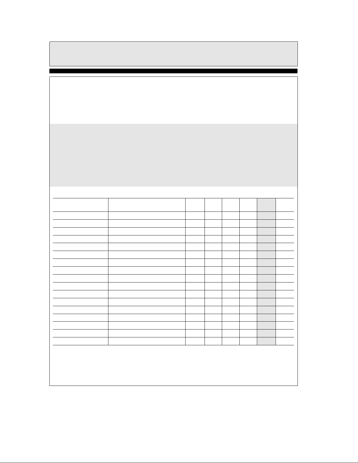
FREQUENCIES and DIVISORS
Function 3Fsc CCIR 601 Square 4Fsc
Divisor 851 864 944 1135
PAL Fosc (MHz) 13.301 13.5 14.75 17.734
Divisor 682 858 780 910
Ý
NTSC Fosc (MHz) 10.738 13.5 12.273 14.318
CCIR 601 Divisors yield 720 pixels in the portion of each line for NTSC and PAL.
Square pixels format gives 640 pixels for NTSC and 768 pixels for PAL in the active portion.
3Fsc numbers do not yield integer divisors.
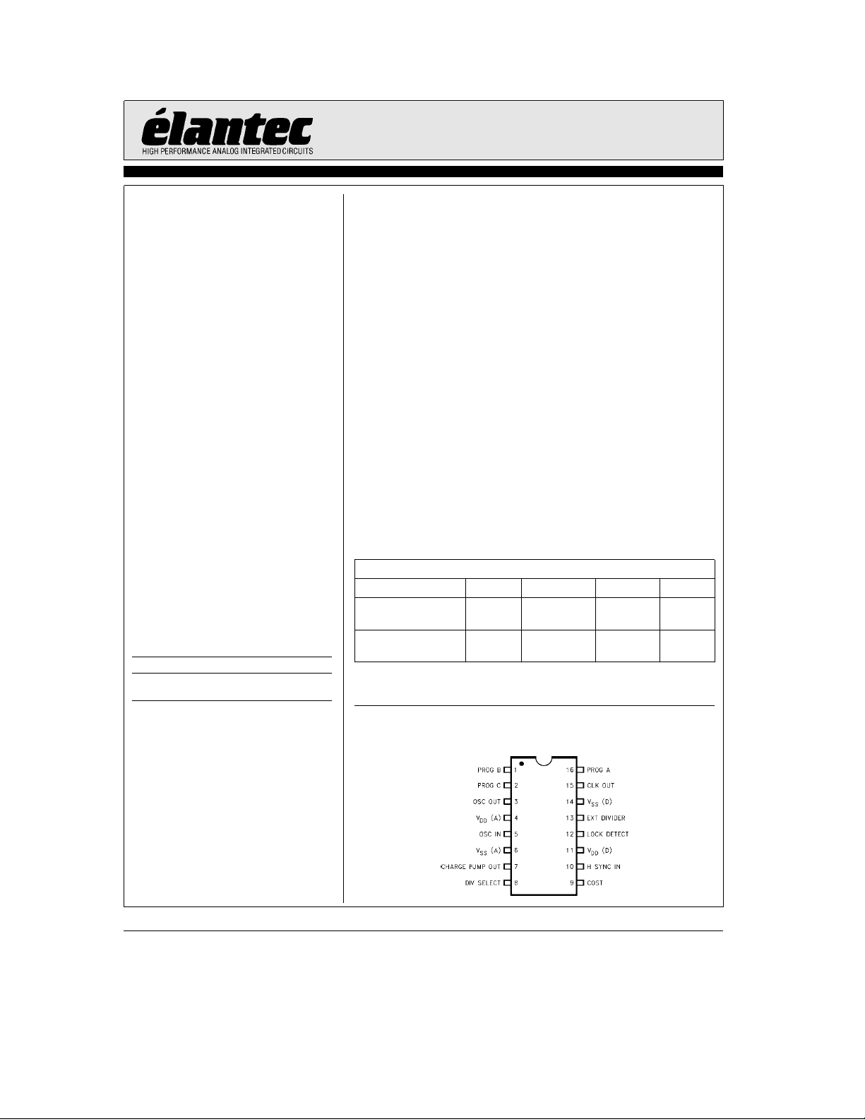
Connection Diagram
EL4584 SO, P-DIP Packages
4584– 17
Note: All information contained in this data sheet has been carefully checked and is believed to be accurate as of the date of publication; however, this data sheet cannot be a ‘‘controlled document’’. Current revisions, if any, to these
specifications are maintained at the factory and are available upon your request. We recommend checking the revision level before finalization of your design documentation.
©
1994 Elantec, Inc.
Ý
4584C
Page 2
EL4584C
Horizontal Genlock, 4 F
SC
Absolute Maximum Ratings
V
Supply 7V Operating Junction Temp 125§C
CC
Storage Temperature
Lead Temperature 260
Pin Voltages
Operating Ambient Temperature
Range
Important Note:
All parameters having Min/Max specifications are guaranteed. The Test Level column indicates the specific device testing actually
performed during production and Quality inspection. Elantec performs most electrical tests using modern high-speed automatic test
equipment, specifically the LTX77 Series system. Unless otherwise noted, all tests are pulsed tests, therefore T
Test Level Test Procedure
I 100% production tested and QA sample tested per QA test plan QCX0002.
II 100% production tested at T
III QA sample tested per QA test plan QCX0002.
IV Parameter is guaranteed (but not tested) by Design and Characterization Data.
V Parameter is typical value at T
T
MAX
and T
MIN
A
per QA test plan QCX0002.
DC Electrical Characteristics
Parameter Conditions Temp Min Typ Max
I
DD
V
Input Low Voltage 25§C 1.5 I V
IL
e
V
5V (Note 1) 25§C24ImA
DD
e
(T
25§C)
A
b
65§Ctoa150§C Power Dissipation 400 mW
b
0.5V to V
b
40§Ctoa85§C
e
25§C and QA sample tested at T
e
25§C for information purposes only.
A
(V
DD
C Oscillator Frequency 36 MHz
§
a
0.5V
CC
e
25§C,
A
e
5V, T
e
25§C unless otherwise noted)
A
e
J
e
T
C
Test
Level
TA.
Units
VIHInput High Voltage 25§C 3.5 I V
IILInput Low Current All inputs except COAST, V
IIHInput High Current All inputs except COAST, V
IILInput Low Current COAST pin, V
IIHInput High Current COAST pin, V
VOLOutput Low Voltage Lock Det, I
VOHOutput High Voltage Lock Det, I
VOLOutput Low Voltage CLK, I
VOHOutput High Voltage CLK, I
OL
OH
VOLOutput Low Voltage OSC Out, I
VOHOutput High Voltage OSC Out, I
IOLOutput Low Current Filter Out, V
IOHOutput High Current Filter Out, V
IOL/IOHCurrent Ratio Filter Out, V
I
Filter Out Coast Mode, V
LEAK
e
1.5V 25§C
IN
e
3.5V 25§C 60 100 I mA
IN
e
1.6mA 25§C 0.4 I V
OL
eb
1.6mA 25§C 2.4 I V
OH
e
3.2mA 25§C 0.4 I V
eb
3.2mA 25§C 2.4 I V
e
200mA25
OL
eb
200mA25
OH
e
2.5V 25§C 200 300 I mA
OUT
e
2.5V 25§C
OUT
e
2.5V 25§C 1.05 1.0 0.95 I
OUT
l
V
DD
OUT
e
1.5V 25§C
IN
e
3.5V 25§C 100 I nA
IN
l
0V 25§C
b
100 I nA
b
C 0.4 I V
§
C 2.4 I V
§
b
b
100
100
60 I mA
b
300b200 I mA
g
1 100 I nA
Note 1: All inputs to 0V, COAST floating.
TDis 3.5in
2
Page 3
EL4584C
Horizontal Genlock, 4 F
TDis 3.5in
SC
AC Electrical Characteristics
Parameter Conditions Temp Min Typ Max
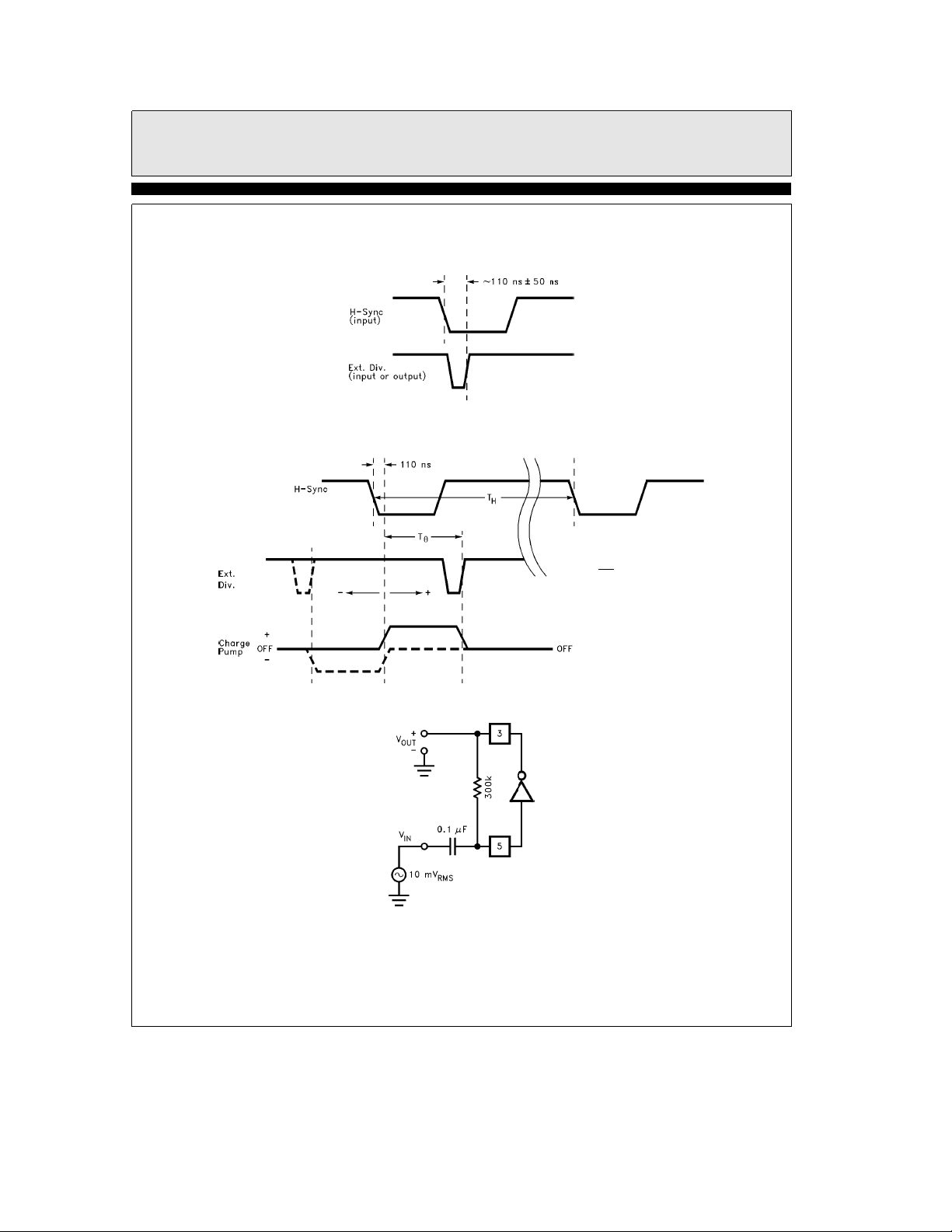
VCO Gain@20 MHz Test Circuit 1 25§C 15.5 V dB
H-sync S/N Ratio V
Jitter VCXO Oscillator 25§C1 Vns
Jitter LC Oscillator (Typ) 25§C10 Vns
Note 2: Noisy video signal input to EL4583C, H-sync input to EL4584C. Test for positive signal lock.
e
5V (Note 2) 25§C35 V dB
DD
e
(V
DD
5V, T
e
25§C unless otherwise noted)
A
Test
Level
Units
Pin Description
Pin No. Pin Name Function
16,1,2 Prog A,B,C Digital inputs to selectdN value for internal counter. See table below for values.
3 Osc/VCO Out Output of internal inverter/oscillator. Connect to external crystal or LC tank VCO circuit.
4VDD(A) Analog positive supply for oscillator, PLL circuits.
5 Osc/VCO In Input from external VCO.
6VSS(A) Analog ground for oscillator, PLL circuits.
7 Charge Pump Out Connect to loop filter. If the H-sync phase is leading or H-sync frequencylCLKdN, current is pumped
8 Div Select Divide select input. When high, the internal divider is enabled and EXT DIV becomes a test pin,
9 Coast Tri-state logic input. Low(k(/3*VCC)enormal mode, Hi Z(or (/3 to )/3*VCC)efast lock mode,
10 H-sync In Horizontal sync pulse (CMOS level) input.
11 VDD(D) Positive supply for digital, I/O circuits.
12 Lock Det Lock Detect output. Low level when PLL is locked. Pulses high when out of lock.
13 Ext Div External Divide input when DIV SEL is low, internaldN output when DIV SEL is high.
14 VSS(D) Ground for digital, I/O circuits.
15 CLK Out Buffered output of the VCO.
into the filter capacitor to increase VCO frequency. If H-sync phase is lagging or frequency
current is pumped out of the filter capacitor to decrease VCO frequency. During coast mode or when
locked, charge pump goes to a high impedance state.
outputting CLK
externaldN.
l
High(
d
N. When low, the internal divider is disabled and EXT DIV is an input from an
)/3*VCC)ecoast mode.
VCO Divisors Table 1
Prog A Prog B Prog C Div Value
Pin 16 Pin 1 Pin 2 N
0 0 0 851
0 0 1 864
0 1 0 944
0 1 1 1135
1 0 0 682
1 0 1 858
1 1 0 780
1 1 1 910
k
CLKdN,
TABWIDE
TDis 3.5in
3
Page 4
EL4584C
Horizontal Genlock, 4 F
Timing Diagrams
PLL Locked Condition (Phase Errore0)
SC
Falling edge of H-synca110 ns locks to rising edge of Ext Div signal.
Out of Lock Condition
Test Circuit 1
4584– 2
T
i
e
i
E
T
H
e
T
H-sync period
H
e
phase error period
T
i
c
360
§
4584– 3
4584– 5
4
Page 5
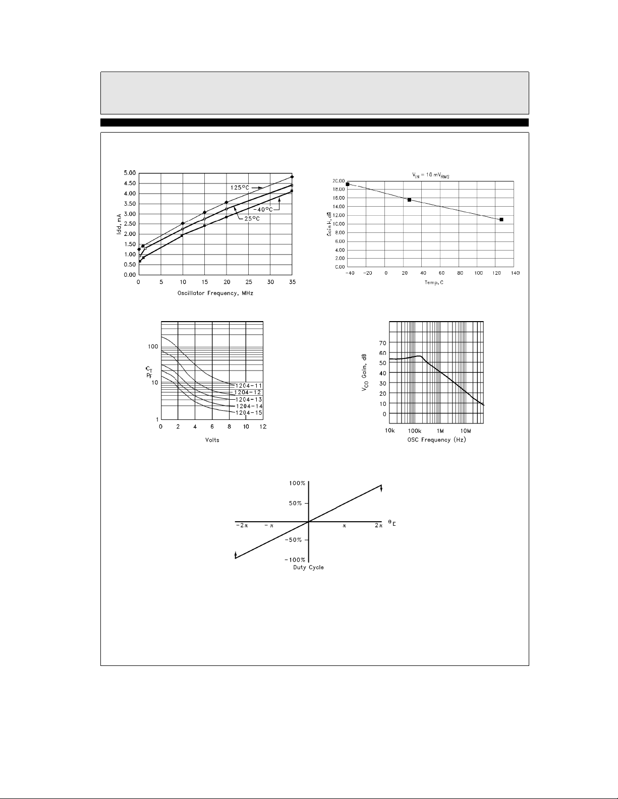
Typical Performance Curves
EL4584C
Horizontal Genlock, 4 F
SC
Idd vs Fosc
Typical Varactor
4584– 4
4584– 7
4584 OSC Gain@20 MHz vs Temp
4584– 6
OSC Gain vs Fosc
4584– 8
Charge Pump Duty Cycle vs i
5
E
4584– 9
Page 6

EL4584C
Horizontal Genlock, 4 F
Block Diagram
SC
4584– 1
6
Page 7

EL4584C
Horizontal Genlock, 4 F
SC
Description Of Operation
The horizontal sync signal (CMOS level, falling
leading edge) is input to H-sync input (pin 10).
This signal is delayed about 110 ns, the falling
edge of which becomes the reference to which the
clock output will be locked. (See timing diagrams.) The clock is generated by the signal on
pin 5, OSC in. There are 2 general types of VCO
that can be used with the EL4584C, LC and crystal controlled. Additionally, each type can be either built up using discrete components, including a varactor as the frequency controlling element, or complete, self contained modules can be
purchased with everything inside a metal can.
The modules are very forgiving of PCB layout,
but cost more than discrete solutions. The VCO
or VCXO is used to generate the clock. An LC
tank resonator has greater ‘‘pull’’ than a crystal
controlled circuit, but will also be more likely to
drift over time, and thus will generate more jitter. The ‘‘pullability’’ of the circuit refers to the
ability to ‘‘pull’’ the frequency of oscillation away
from its center frequency by modulating the voltage on the control pin of a VCO module or varactor, and is a function of the slope and range of
the capacitance-voltage curve of the varactor or
VCO module used. The VCO signal is sent to a
divide by N counter, and to the CLK out pin. The
divisor N is determined by the state of pins 1,2,
and 16 and is described in table 1 above. The divided signal is sent, along with the delayed
H-sync input, to the phase/frequency detector,
which compares the two signals for phase and
frequency differences. Any phase difference is
converted to a current at the charge pump output
FILTER (pin 7). A VCO with positive frequency
deviation with control voltage must be used. Varactors have negative capacitance slope with
voltage, resulting in positive frequency deviation
with control voltage for the oscillators in figures
10 and 11 below.
VCO
The VCO should be tuned so its frequency of oscillation is very close to the required clock output
frequency when the voltage on the varactor is 2.5
volts. VCXO and VCO modules are already tuned
to the desired frequency, so this step is not necessary if using one of these units. The range of the
charge pump output (pin 7) is 0 to 5 volts and it
can source or sink a maximum of about 300 mA,
so all frequency control must be accomplished
with variable capacitance from the varactor within this range. Crystal oscillators are more stable
than LC oscillators, which translates into lower
jitter, but LC oscillators can be pulled from their
mid-point values further, resulting in a greater
capture and locking range. If the incoming horizontal sync signal is known to be very stable,
then a crystal oscillator circuit can be used. If the
h-sync signal experiences frequency variations of
greater than about 300 ppm, an LC oscillator
should be considered, as crystal oscillators are
very difficult to pull this far. When H-SYNC input frequency is greater than CLK frequen-
d
cy
N, charge pump output (pin 7) sources current into the filter capacitor, increasing the voltage across the varactor, which lowers its capacitance, thus tending to increase VCO frequency.
Conversely, filter output pulls current from the
filter capacitor when H-SYNC frequency is less
than CLK
d
N, forcing the VCO frequency lower.
Loop Filter
The loop filter controls how fast the VCO will
respond to a change in filter output stimulus. Its
components should be chosen so that fast lock
can be achieved, yet with a minimum of VCO
‘‘hunting’’, preferably in one to two oscillations
of charge pump output, assuming the VCO frequency starts within capture range. If the filter is
under-damped, the VCO will over and undershoot the desired operating point many times before a stable lock takes place. It is possible to
under-damp the filter so much that the loop itself
oscillates, and VCO lock is never achieved. If the
filter is over-damped, the VCO response time will
be excessive and many cycles will be required for
a lock condition. Over-damping is also characterized by an easily unlocked system because the
filter can’t respond fast enough to perturbations
in VCO frequency. A severely over damped system will seem to endlessly oscillate, like a very
large mass at the end of a long pendulum. Due to
parasitic effects of PCB traces and component
variables, it will take some trial and error experimentation to determine the best values to use for
any given situation. Use the component tables as
a starting point, but be aware that deviation from
these values is not out of the ordinary.
7
Page 8

EL4584C
Horizontal Genlock, 4 F
SC
Description of Operation
Ð Contd.
External Divide
DIV SEL (pin 8) controls the use of the internal
divider. When high, the internal divider is enabled and EXT DIV (pin 13) outputs the CLK
out divided by N. This is the signal to which the
horizontal sync input will lock. When divide select is low, the internal divider output is disabled,
and external divide becomes an input from an external divider, so that a divisor other than one of
the 8 pre-programmed internal divisors can be
used.
Normal Mode
Normal mode is enabled by pulling COAST (pin
9) low (below (/3*V
have any phase or frequency difference, an error
signal is generated and sent to the charge pump.
The charge pump will either force current into or
out of the filter capacitor in an attempt to modulate the VCO frequency. Modulation will continue until the phase and frequency of CLK
actly match the H-sync input. When the phase
and frequency match (with some offset in phase
that is a function of the VCO characteristics), the
error signal goes to zero, lock detect no longer
pulses high, and the charge pump enters a high
impedance state. The clock is now locked to the
H-sync input. As long as phase and frequency
differences remain small, the PLL can adjust the
VCO to remain locked and lock detect remains
low.
). If H-sync and CLKdN
CC
d
N ex-
Fast Lock Mode
Fast Lock mode is enabled by either allowing
coast to float, or pulling it to mid supply (between (/3 and )/3*V
achieved much faster than in normal mode, but
the clock divisor is modified on the fly to achieve
this. If the phase detector detects an error of
enough magnitude, the clock is either inhibited
or reset to attempt a ‘‘fast’’ lock of the signals.
). In this mode, lock is
CC
Forcing the clock to be synchronized to the Hsync input this way allows a lock in approximately 2 H-cycles, but the clock spacing will not be
regular during this time. Once the near lock condition is attained, charge pump output should be
very close to its lock-on value and placing the
device into normal mode should result in a normal lock very quickly. Fast Lock mode is intended to be used where H-sync becomes irregular,
until a stable signal is again obtained.
Coast Mode
Coast mode is enabled by pulling COAST (pin 9)
high (above )/3*V
phase detector is disabled and filter out remains
in high impedance mode to keep filter out voltage and VCO frequency as constant a possible.
VCO frequency will drift as charge leaks from the
filter capacitor, and the voltage changes the VCO
operating point. Coast mode is intended to be
used when noise or signal degradation result in
loss of horizontal sync for many cycles. The
phase detector will not attempt to adjust to the
resultant loss of signal so that when horizontal
sync returns, sync lock can be re-established
quickly. However, if much VCO drift has occurred, it may take as long to re-lock as when
restarting.
). In coast mode the internal
CC
Lock Detect
Lock detect (pin 12) will go low when lock is established. Any DC current path from charge
pump out will skew EXT DIV relative to
H-SYNC in, tending to offset or add to the 110 ns
internal delay, depending on which way the extra
current is flowing. This offset is called static
phase error, and is always present in any PLL
system. If, when the part stabilizes in a locked
mode, lock detect is not low, adding or subtracting from the loop filter series resistor R
change this static phase error to allow LDET to
go low while in lock. The goal is to put the rising
edge of EXT DIV in sync with the falling edge of
H-SYNC
creasing R
ing R
tive when EXT DIV lags H-SYNC.) The resistance needed will depend on VCO design or VCXO
module selection.
a
110 ns. (See timing diagrams.) In-
decreases phase error, while decreas-
2
increases phase error. (Phase error is posi-
2
will
2
8
Page 9

EL4584C
Horizontal Genlock, 4 F
SC
Applications Information
Choosing External Components
1. To choose LC VCO components, first pick the
desired operating frequency. For our example
we will use 14.31818 MHz, with an H-sync frequency of 15.734 kHz.
2. Choose a reasonable inductor value (10–20mH
works well). We choose 15 mH.
3. Calculate C
e
F
OSC
e
C
T
4q2F2L
4. From the varactor data sheet find C
the desired lock voltage. C
SMV1204-12, for example.
5. C
should be about 10CV, so we choose
2
e
C
220 pF for our example.
2
6. Calculate C
e
C
T
(C1C2)a(C1CV)a(C2CV)
then
needed to produce F
T
1
2q0LC
T
1
e
4q2(14.318e6)2(15eb6)
. Since
1
C1C2C
V
.
OSC
1
e
V
e
8.2 pF
@
2.5V,
V
23 pF for our
,
Typical LC VCO
4584– 10
Figure 10
LC VCO Component Values (Approximate)
Frequency L1 C1 C2
(MHz) (mH) (pF) (pF)
13.301 15 18 220
13.5 15 17 220
14.75 12 18 220
17.734 12 10 220
10.738 22 20 220
12.273 18 17 220
14.318 15 14 220
Note: Use shielded inductors for optimum performance.
Typical Xtal VCO
C2CTC
e
C
1
(C2CV)b(C2CT)b(CTCV)
For our example, C
V
e
14 pF. (A trim cap may be
1
.
used for fine tuning.) Examples for each frequency using the internal divider follow.
Typical Application
Horizontal genlock provides clock for an analog
to digital converter, digitizing analog video.
Figure 11
4584– 11
4584– 18
9
Page 10

EL4584C
Horizontal Genlock, 4 F
SC
Xtal VCO Component Values (Approximate)
Frequency R1 C1 C2
(MHz) (kX) (pF) (uF)
13.301 300 15 .001
13.5 300 15 .001
14.75 300 15 .001
17.734 300 15 .001
10.738 300 15 .001
12.273 300 15 .001
14.318 300 15 .001
The above oscillators are arranged as Colpitts oscillators, and the structure is redrawn here to emphasize the split capacitance used in a Colpitts
oscillator. It should be noted that this oscillator
configuration is just one of literally hundreds
possible, and the configuration shown here does
not necessarily represent the best solution for all
applications. Crystal manufacturers are very informative sources on the design and use of oscillators in a wide variety of applications, and the
reader is encouraged to become familiar with
them.
Colpitts Oscillator
Choosing Loop Filter
Components
The PLL, VCO, and loop filter can be described
as:
4584– 13
Where:
e
K
phase detector gain in A/rad
d
e
F(s)
loop filter impedance in V/A
e
K
N
It can be shown that for the loop filter shown
below:
C
Where 0
filter damping factor.
1. K
VCO gain in rad/s/V
VCO
e
internal or external divisor
KdK
VCO
e
3
d
2
N0
n
e
loop filter bandwidth, and geloop
n
e
300 mA/2qrade4.77e-5A/rad for the
,C
C
3
e
4
10
EL4584C.
,R
2Ng0
KdK
n
VCO
e
3
4584– 12
C1is to adjust the center frequency, C2DC isolates the control from the oscillator, and V1 is the
primary control device. C
than C
so that V1has maximum modulation
V
should be much larger
2
capability. The frequency of oscillation is given
by:
1
e
F
2q0LC
T
C1C2C
e
C
T
(C1C2)a(C1CV)a(C2CV)
V
2. The loop bandwidth should be about H-sync
frequency/20, and the damping ratio should be
1 for optimum performance. For our example,
e
0
15.734 kHz/20e787 Hz&5000 rad/S.
n
e
3. N
910 from table 1.
VCOfrequency
e
N
H-SYNCfrequency
4. K
represents how much the VCO frequen-
VCO
14.31818M
e
15.73426k
e
cy changes for each volt applied at the control
pin. It is assumed (but probably isn’t) linear
about the lock point (2.5V). Its value depends
on the VCO configuration and the varactor
10
910
Page 11

EL4584C
Horizontal Genlock, 4 F
SC
transfer function C
reverse bias control voltage, and C
capacitance. Since F(V
e
F(VC), where VCis the
v
) is nonlinear, it is
C
is varactor
V
probably best to build the VCO and measure
K
about 2.5V. The results of one such mea-
VCO
surement are shown below. The slope of the
curve is determined by linear regression techniques and equals K
e
K
VCO
6.05 Mrad/S/V.
F
vs VC,LCVCO
OSC
. For our example,
VCO
5. Now we can solve for C3,C4, and R3.
KdK
e
C
3
N0
C
3
e
C
4
10
2Ng0
e
R
3
KdK
We choose R
6. Notice R
sign. R
VCO
e
2
(4.77eb5)(6.05e6)
e
2
n
(910)(5000)
e
2
0.01 mF
0.001 mF
(2)(910)(1)(5000)
n
e
(4.77eb5)(6.05e6)
VCO
e
30 kX for convenience.
3
has little effect on the loop filter de-
2
e
31.5 kX
should be large, around 100k, and can
be adjusted to compensate for any static phase
error T
slow loop response. If R
at lock, but if made too large, will
i
is made smaller, T
2
(see timing diagrams) increases, and if R2increases, T
lock,
decreases. For LDET to be low at
i
k
T
50 ns. C4is used mainly to attenu-
l
l
i
ate high frequency noise from the charge
pump.
4584– 14
Lock Time
Let SeR3C3. As T increases, damping increases,
but so does lock time. Decreasing T decreases
damping and speeds up loop response, but increases overshoot and thus increases the number
of hunting oscillations before lock. Critical damp-
e
ing (g
decreased damping also decreases loop stability,
it is sometimes desirable to design slightly overdamped (g
stability.
i
1) occurs at minimum lock time. Because
l
1), trading lock time for increased
Typical Loop Filter
LC Loop Filter Components (Approximate)
Frequency R2 R3 C3 C4
(MHz) (kX)(kX)(mF) (mF)
13.301 100 30 0.01 0.001
13.5 100 30 0.01 0.001
14.75 100 33 0.01 0.001
17.734 100 39 0.01 0.001
10.738 100 22 0.01 0.001
12.273 100 27 0.01 0.001
14.318 100 30 0.01 0.001
Xtal Loop Filter Components (Approximate)
Frequency R2 R3 C3 C4
(MHz) (kX)(MX) (pF) (pF)
13.301 100 4.3 68 6.8
13.5 100 4.3 68 6.8
14.75 100 4.3 68 6.8
17.734 100 4.3 68 6.8
10.738 100 4.3 68 6.8
12.273 100 4.3 68 6.8
14.318 100 4.3 68 6.8
4584– 16
11
Page 12

EL4584C
Horizontal Genlock, 4 F
SC
PCB Layout Considerations
It is highly recommended that power and ground
planes be used in layout. The oscillator and filter
sections constitute a feedback loop and thus care
must be taken to avoid any feedback signal influencing the oscillator except at the control input.
The entire oscillator/filter section should be surrounded by copper ground to prevent unwanted
influences from nearby signals. Use separate
paths for analog and digital supplies, keeping the
analog (oscillator section) as short and free from
spurious signals as possible. Careful attention
must be paid to correct bypassing. Keep lead
lengths short and place bypass caps as close to
the supply pins as possible. If laying out a PCB
to use discrete components for the VCO section,
care must be taken to avoid parasitic capacitance
at the OSC pins 3 and 5, and FILTER out (pin
7). Remove ground and power plane copper
above and below these traces to avoid making a
capacitive connection to them. It is also recommended to enclose the oscillator section within a
shielded cage to reduce external influences on the
VCO, as they tend to be very sensitive to ‘‘handwaving’’ influences, the LC variety being more
sensitive than crystal controlled oscillators. In
general, the higher the operating frequency, the
more important these considerations are. Self
contained VCXO or VCO modules are already
mounted in a shielding cage and therefore do not
require as much consideration in layout. Many
crystal manufacturers publish informative literature regarding use and layout of oscillators which
should be helpful.
12
Page 13

EL4584C
Horizontal Genlock, 4 F
SC
Demo Board
4584– 19
13
Page 14

EL4584C
Horizontal Genlock, 4 F
The VCO and loop filter section of the EL4583/4/5 demo board can be implemented in the following
configurations:
SC
(1) VCXO
4584– 20
(2) XTAL
(3) LC Tank
14
4584– 21
4584– 22
Page 15

BLANK
15
Page 16

EL4584C
Horizontal Genlock, 4 F
EL4584CFebruary 1995 Rev B
SC
Component Sources
Inductors
Dale Electronics
#
Crystals, VCXO, VCO Modules
#
#
#
E. Highway 50
PO Box 180
Yankton, SD 57078-0180
(605) 665-9301
Connor-Winfield
2111 Comprehensive Drive
Aurora, IL 60606
(708) 851-4722
Piezo Systems
100 K Street
PO Box 619
Carlisle, PA 17013
(717) 249-2151
Reeves-Hoffman
400 West North Street
Carlisle, PA 17013
(717) 243-5929
SaRonix
#
#
151 Laura Lane
Palo Alto, CA 94043
(415) 856-6900
Standard Crystal
9940 Baldwin Place
El Monte, CA 91731
(818) 443-2121
Varactors
Alpha Industries
#
#
Note: These sources are provided for information
purposes only. No endorsement of these companies is implied by this listing.
20 Sylvan Road
Woburn, MA 01801
(617) 935-5150
Motorola Semiconductor Products
2100 E. Elliot
Tempe, AZ 85284
(602) 244-6900
General Disclaimer
Specifications contained in this data sheet are in effect as of the publication date shown. Elantec, Inc. reserves the right to make changes
in the circuitry or specifications contained herein at any time without notice. Elantec, Inc. assumes no responsibility for the use of any
circuits described herein and makes no representations that they are free from patent infringement.
WARNING Ð Life Support Policy
Elantec, Inc. products are not authorized for and should not be
used within Life Support Systems without the specific written
consent of Elantec, Inc. Life Support systems are equipment in-
Elantec, Inc.
1996 Tarob Court
Milpitas, CA 95035
Telephone: (408) 945-1323
(800) 333-6314
Fax: (408) 945-9305
European Office: 44-71-482-4596
tended to support or sustain life and whose failure to perform
when properly used in accordance with instructions provided can
be reasonably expected to result in significant personal injury or
death. Users contemplating application of Elantec, Inc. products
in Life Support Systems are requested to contact Elantec, Inc.
factory headquarters to establish suitable terms & conditions for
these applications. Elantec, Inc.’s warranty is limited to replacement of defective components and does not cover injury to persons or property or other consequential damages.
Printed in U.S.A.16
 Loading...