

Page 1
EL4583C
Sync Separator, 50% Slice, S-H, Filter, H
EL4583C
OUT
Features
• NTSC, PAL, and SECAM sync
separation
• Single supply, +5V operation
• Precision 50% slicing
• Built-in programmable color burst
filter
• Decodes non-standard vertical
• Horizontal sync output
• Sync. pulse amplitude output
• Same socket can be used for 8-pin
EL4581C
• Low-power CMOS
• Detects loss of signal
• Resistor programmable scan rate
• Few external components
• Available in 16-pin PDIP and 16pin SO (0.150”) packages
Applications
• Video special effects
• Video test equipment
• Video distribution
• Multimedia
• Displays
• Imaging
• Video data capture
• Video triggers
Ordering Information
Part No Package
EL4583CN 16-Pin PDIP - MDP0031
EL4583CS 16-Pin SO (0.150”) - MDP0027
EL4583CS-T7 16-Pin SO (0.150”) 7” MDP0027
EL4583CS-T13 16-Pin SO (0.150”) 13” MDP0027
Tape &
Reel Outline #
General Description
The EL4583C extracts timing from video sync in NTSC, PAL, and
SECAM systems, and non standard formats, or from computer graphics operating at higher scan rates. Timing adjustment is via an external
resistor. Input without valid vertical interval (no serration pulses) produces a default vertical output.
Outputs are: composite sync, vertical sync, filter, burst/back porch,
horizontal, no signal detect, level, and odd/even output (in interlaced
scan formats only).
The EL4583C sync slice level is set to the mid-point between sync tip
and the blanking level. This 50% point is determined by two internal
sample and hold circuits that track sync tip and back porch levels. It
provides hum and noise rejection and compensates for input levels of
0.5V to 2.0V
P-P
.
A built in filter attenuates the chroma signal to prevent color burst
from disturbing the 50% sync slice. Cut off frequency is set by a resistor to ground from the Filter Cut Off pin. Additionally, the filter can be
by-passed and video signal fed directly to the Video Input.
The level output pin provides a signal with twice the sync amplitude
which may be used to control an external AGC function. A
TTL/CMOS compatible No Signal Detect Output flags a loss or reduction in input signal level. A resistor sets the Set Detect Level.
The EL4583C is manufactured using Elantec’s high performance analog CMOS process.
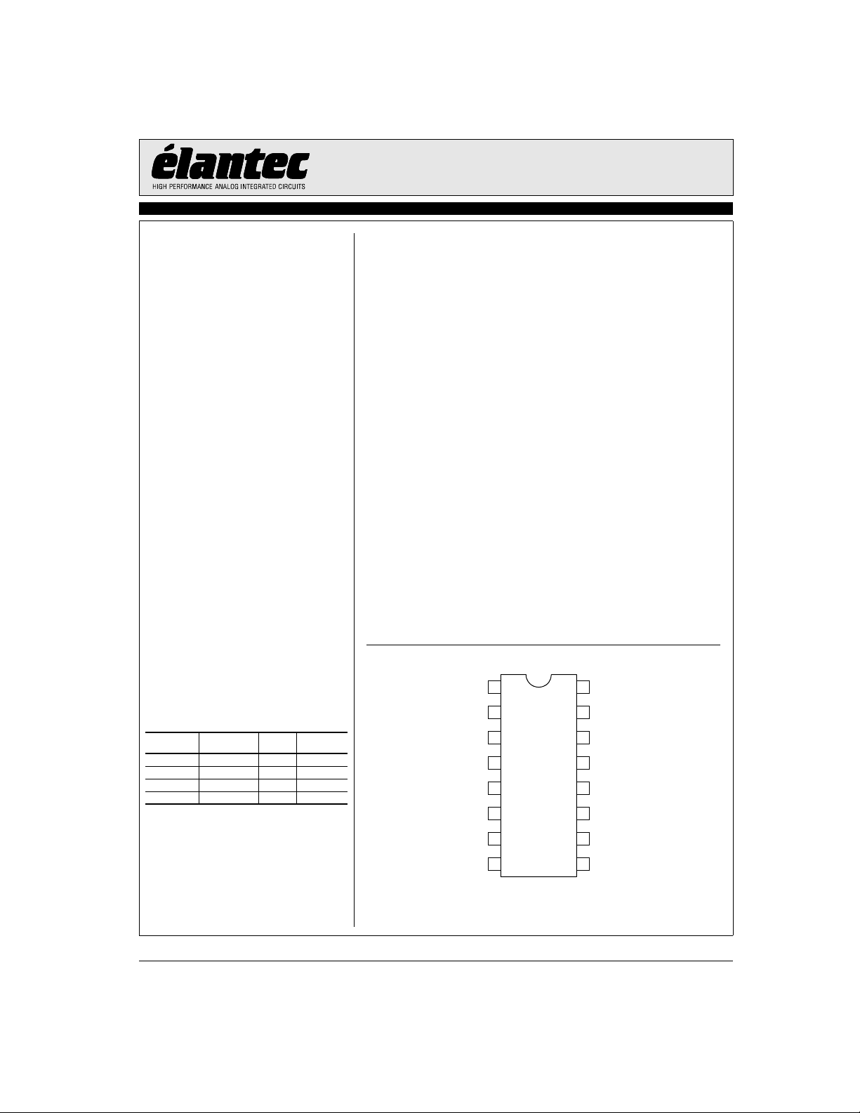
Connection Diagram
FILTER CUT OFF
SET DETECT LEVEL
COMPOSITE SYNC OUT
FILTER INPUT
VERTICAL SYNC OUT
DIGITAL GND
FILTER OUTPUT
1
2
3
4
5
6
7
16
ANALOG GND
15
HORIZONTAL SYNC OUT
14
VDD
13
ODD/EVEN OUTPUT
12
RSET*
11
BURST/BACK PORCH OUTPUT
10
NO SIGNAL DETECT OUTPUT
August 6, 2001
COMPOSITE VIDEO INPUT
*Note: RSET must be a 1% register
Manufactured under US Patent 5,528,303
Note: All information contained in this data sheet has been carefully checked and is believed to be accurate as of the date of publication; however, this data sheet cannot be a “controlled document”. Current revisions, if any, to these
specifications are maintained at the factory and are available upon your request. We recommend checking the revision level before finalization of your design documentation.
© 2001 Elantec Semiconductor, Inc.
8 9
EL4583C
(8-Pin SO & 8-Pin PDIP)
LEVEL OUTPUT
Page 2
EL4583C
Sync Separator, 50% Slice, S-H, Filter, H
EL4583C
OUT
Absolute Maximum Ratings (T
VCC Supply 7V
Storage Temperature -65°C to +150°C
Pin Voltages -0.5V to VCC +0.5V
Important Note:
All parameters having Min/Max specifications are guaranteed. Typ values are for information purposes only. Unless otherwise noted, all tests are at the
specified temperature and are pulsed tests, therefore: TJ = TC = TA.
= 25°C)
A
Operating Temperature Range -40°C to +85°C
Power Dissipation See Curves
Die Junction Temperature 150°C
DC Electrical Characteristics
VDD = 5V, TA = 25°C, R
I
DD
Clamp Voltage Pins 4, 8, unloaded 1.3 1.55 1.8 V
Discharge Current Pins 4, 8, with Signal (VIN = 2V) 3 6 12 µA
Discharge Current Pins 4, 8, no Signal
Clamp Charge Current Pins 4, 8, VIN = 1V 2 3 4 mA
Ref. Voltage V
Filter Reference Voltage, VRF Pin 1 0.35 0.5 0.65 V
Level Reference Current Pin 2
VOL Output Low Voltage IOL = 1.6mA 350 800 mV
VOH Output High Voltage
1. No video signal, outputs unloaded
2. At loss of signal (pin 10 high) the pull down current source switches to a value of 10µA
3. Tested for VDD 5V ±5%
4. Current sourced from pin 2 is V
REF
= 681kΩ, RF = 22kΩ, RLV = 82kΩ
SET
Parameter Description Min Typ Max Unit
REF/RSET
[1]
VDD = 5V
[2]
Pin 12, VDD = 5V
[4]
IOH = -40µA 4
IOH = -1.6mA 2.4 4
[3]
1.5 1.75 2 V
1.5 2.5 3.5 µA
2.5 4 mA
10 µA
V
2
Page 3
EL4583C
Sync Separator, 50% Slice, S-H, Filter, H
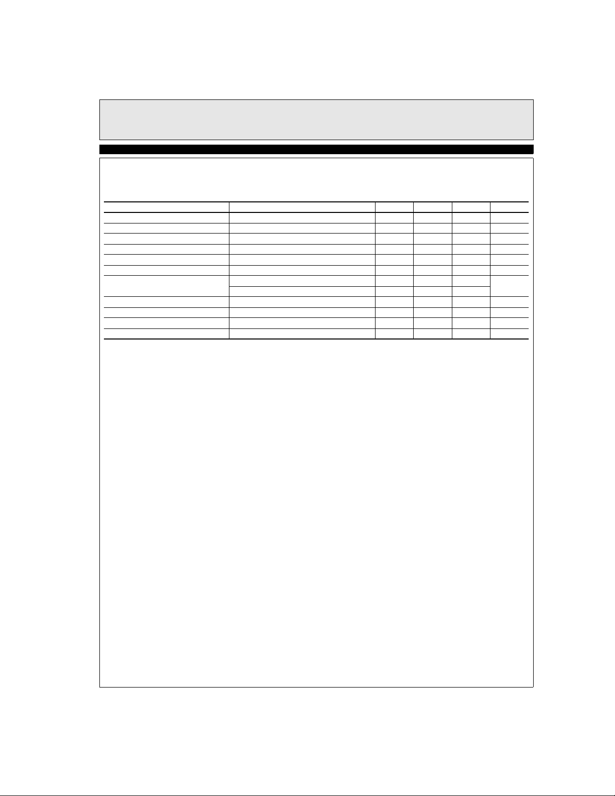
Dynamic Characteristics
R
= 22kΩ, R
F
Horizontal Pulse Width, Pin 15, t
Vertical Sync Width, Pin 5, t
Burst/Back Porch Width, Pin 11, t
Filter Attenuation FIN = 3.6MHz
Comp. Sync Prop. Delay, t
Input Dynamic Range p-p NTSC Signal 0.4 2 V
Slice Level
Level Out, Pin 9 Input Voltage = 1V
Vertical Sync Default Time, t
Loss of Signal Time-Out Pin 10 400 600 800 µs
Burst/Back Porch Delay, t
1. Width is a function of R
2. c/s, Vertical, Back porch and H are all active low, VOH = 0.8V; vertical is 3H lines wide of NTSC signal
3. Attenuation is a function of RF. See filter typical characteristics
4. Vertical pulse width in absence of serrations on input signal
= 681kΩ, V
SET
Parameter Description Min Typ Max Unit
= 5V, Video Input = 1V
DD
H
VS
B
CS
VSD
BD
SET
, TA = 25°C, CL = 15pF, IOH = -1.6mA, IOL = 1.6mA
P-P
[1]
[2]
[1]
VIN (Pin 4)—Comp Sync 250 400 ns
Input Voltage = 1V
V
SLICE/VBLANK
[4]
See Figure 4 250 400 ns
[3]
p-p
Pin 4 500 600 700 mV
p-p,
3.8 5 6.2 µs
195 µs
2.7 3.7 4.7 µs
12 dB
40 50 60
40 50 60
27 36 57 µs
EL4583C
OUT
%
3
Page 4
EL4583C
Sync Separator, 50% Slice, S-H, Filter, H
EL4583C
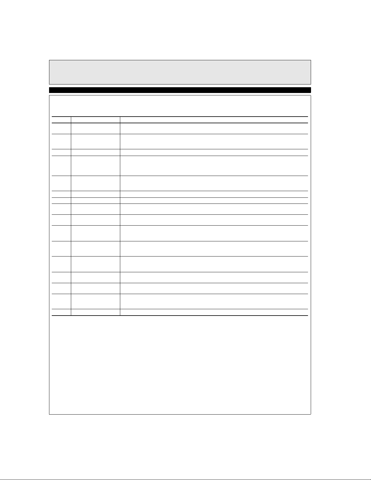
Pin Descriptions
Pin No. Pin Name Function
1 Filter Cut-Off A resistor RF connected between this input and ground determines the input filter characteristic. Increasing RF
2 Set Detect Level A resistor RLV connected between pin 2 and ground determines the value of the minimum signal which triggers the
3 Composite Sync Output This output replicates all the sync inputs on the input video.
4 Filter Input The filter is a 3 pole active filter with a gain of 2, designed to produce a constant phase delay of nominally 260ns with
5 Vertical Sync Output The vertical sync output is synchronous with the first serration pulse rising edge in the vertical interval of the input
6 Digital Ground This is the ground return for digital buffer outputs.
7 Filter Output Output of the active 3 pole filter which has its input on pin 4. It is recommended to ac couple the output to pin 8.
8 Video Input This input can be directly driven by the signal if it is desired to bypass the filter, for example, in the case of strong
9 Level Output This pin provides an analog voltage which is nominally equal to twice the sync pulse amplitude of the video input sig-
10 No Signal Detect Output This is a digital output which goes high when either a) loss of input signal or b) the input signal level falls below a pre-
11 Burst/Back Porch Output The start of back porch output is triggered on the trailing edge of normal H sync, and on the rising edge of serration
12 RSET The current through the resistor RSET determines the timing of the functions within the I.C. These functions include
13 Odd/Even Output Odd-even output is low for even field and high for odd field. The operation of this circuit has been improved for reject-
14 VDD 5V The internal circuits are designed to have a high immunity to supply variations, although as with most I.C.s a 0.1µF
15 Horizontal Sync Output This output produces only true H pulses of nominal width 5µs. The leading edge is triggered from the leading edge of
16 Analog Ground This is the ground return for the signal paths in the chips, RSET, RF and RLV.
increases the filter 3.58MHz color burst attenuation. See the typical performance characteristics.
loss of signal output on pin 10. The relationship is VPMIN = 0.75RLV/RSET, where VPMIN is the minimum detected
sync pulse amplitude applied to pin 4. See the typical performance characteristics.
signal amplitude. Resistor RF on pin 1 controls the filter cut-off. An internal clamp sets the minimum voltage on pin
4 at 1.55V when the input becomes low impedance. Above the clamp voltage, an input current of 1µA charges the
input coupling capacitor. With loss of signal, the current source switches to a value of 10µA, for faster signal recovery.
signal and ends on the trailing edge of the first equalizing Output pulse after the vertical interval. It will therefore be
slightly more than 3H lines wide.
clean signals. This input is 6dB less sensitive than the filter input.
nal applied to pin 4. It therefore provides an indication of signal strength.
determined amplitude as set by RLV on pin 2. There will be several horizontal lines delay before the output is
initiated.
pulses in the vertical interval. The pulse is timed out internally to produce a one-shot output. The pulse width is a function of RSET. This output can be used for d.c. restore functions where the back porch level is a known reference.
the sampling of the sync pulse 50% point, back porch output and the 2H eliminator. For faster scan rates, the resistor
needs to be reduced inversely. For NTSC 15.7kHz scan rate RSET is 681k 1%. RSET must be a 1% resistor.
ing spurious noise pulses such as those present in VCR signals.
decoupling capacitor is advisable.
the input H sync, with the same prop. delay as the composite sync. The half line pulses present in the input signal during vertical blanking are eliminated with an internal 2H eliminator circuit.
OUT
4
Page 5

Typical Performance Curves
EL4583C
Sync Separator, 50% Slice, S-H, Filter, H
EL4583C
OUT
RSET vs
Horizontal Frequency
Filter 3dB BW vs RF Level Out (Pin 9) vs
Back Porch Clamp
On Time vs RSET
Sync. Tip Amplitude
Vertical Default Delay
Time vs RSET
Minimum Signal Detect
vs RLV
Package Power Dissipation vs Ambient Temp.
Filter Attenuation vs RF @
f = 3.58MHz
Note 1: For RLV < 1000k¾, no signal detect output (pin 10) will default high at minimum signal sensitivity specification, or at complete loss of signal.
JEDEC JESD51-3 Low Effective Thermal Conductivity Test Board
1.8
1.54W
1.6
1.4
1.136W
1.2
1
0.8
0.6
Power Dissipation (W)
0.4
0.2
0
0 25 50 75 100 125 150
P
D
I
P
θ
1
J
6
A
=
8
1
°
C
/
W
S
O
1
θ
J
A
=
1
1
0
°
C
Ambient Temperature (°C)
6
/
W
85
5
Page 6

EL4583C
Sync Separator, 50% Slice, S-H, Filter, H
EL4583C
Timing Diagram
OUT
Notes:
b. The composite sync output reproduces all the video input sync pulses, with a propagation delay.
c. Vertical sync leading edge is coincident with the first vertical serration pulse leading edge, with a propagation delay.
d. Odd-even output is low for even field, and high for odd field.
e. Back porch goes low for a fixed pulse width on the trailing edge of video input sync pulses. Note that for serration pulses during vertical, the back porch starts on the rising edge
of the serration pulse (with propagation delay).
f. Horizontal sync output produces the true “H” pulses of nominal width of 5µs. It has the same delay as the composite sync.
Figure 1.
6
Page 7

EL4583C
Sync Separator, 50% Slice, S-H, Filter, H
EL4583C
OUT
Figure 2.
Figure 3.
7
Page 8

EL4583C
Sync Separator, 50% Slice, S-H, Filter, H
EL4583C
OUT
Figure 4. Standard (NTSC Input) H. Sync Detail
8
Page 9

Description of Operation
A simplified block schematic is shown in Figure 1. The
following description is intended to provide the user
with sufficient information to understand the effects of
the external components and signal conditions on the
outputs of the integrated circuit.
The video signal is AC coupled to pin 4 via the capacitor
C1, nominally 0.1µF. The clamp circuit A1 will prevent
the input signal on pin 4 going more negative than 1.5V,
the value of reference voltage VR1. Thus the sync tip, the
most negative part of the video waveform, will be
clamped at 1.5V. The current source I1, nominally 6µA,
charges the coupling capacitor during the remaining portion of the H line, approximately 58µs for a 15.75kHz
timebase. From I • t = C • V, the video time-constant can
be calculated. It is important to note that the charge
taken from the capacitor during video must be replaced
during the sync tip time, which is much shorter, (ratio of
x 12.5). The corresponding current to restore the charge
during sync will therefore be an order of magnitude
higher, and any resistance in series with CI will cause
sync tip crushing. For this reason, the internal series
resistance has been minimized and external high resistance values in series with the input coupling capacitor
should be avoided. The user can exercise some control
over the value of the input time constant by introducing
an external pull-up resistance from pin 4 to the 5V supply. The maximum voltage across the resistance will be
VDD less 1.5V, for black level. For a net discharge current greater than zero, the resistance should be greater
than 450k. This will have the effect of increasing the
time constant and reducing the degree of picture tilt. The
current source I1 directly tracks reference current I
and thus increases with scan rate adjustment, as
explained later.
The signal is processed through an active 3 pole filter
(F1) designed for minimum ripple with constant phase
delay. The filter attenuates the color burst by 12dB and
eliminates fast transient spikes without sync crushing.
An external filter is not necessary. The filter also amplifies the video signal by 6dB to improve the detection
accuracy. The filter cut-off frequency is controlled by an
external resistor from pin 1 to ground.
Internal reference voltages (block V
immunity to supply voltage variation are derived on the
) with high
REF
TR
EL4583C
Sync Separator, 50% Slice, S-H, Filter, H
chip. Reference VR4 with op-amp A2 forces pin 12 to a
reference voltage of 1.7V nominal. Consequently, it can
be seen that the external resistance RSET will determine
the value of the reference current ITR. The internal resis-
tance R3 is only about 6kΩ, much less than RSET. All
the internal timing functions on the chip are referenced
to ITR and have excellent supply voltage rejection.
To improve noise immunity, the output of the 3 pole filter is brought out to pin 7. It is recommended to AC
couple the output to pin 8, the video input pin. In case of
strong clean video signal, the video input pin, pin 8, can
be driven by the signal directly.
Comparator C2 on the input to the sample and hold
block (S/H) compares the leading and trailing edges of
the sync. pulse with a threshold voltage VR2 which is
referenced at a fixed level above the clamp voltage VR1.
The output of C2 initiates the timing one-shots for gating
the sample and hold circuits. The sample of the sync tip
is delayed by 0.8µs to enable the actual sample of 2µs to
be taken on the optimum section of the sync. pulse tip.
The acquisition time of the circuit is about three horizontal lines. The double poly CMOS technology enables
long time constants to be achieved with small high quality on-chip capacitors. The back porch voltage is
similarly derived from the trailing edge of sync, which
also serves to cut off the tip sample if the gate time
exceeds the tip period. Note that the sample and hold
gating times will track RSET through IOT.
The 50% level of the sync tip is derived through the
resistor divider R1 and R2, from the sample and held
voltages V
comparator C1. This comparator has built in hysteresis
to avoid false triggering. The output of C2 is a digital 5V
signal which feeds the C/S output buffer B1, the vertical,
back porch and odd/even functions.
The vertical circuit senses C/S edges and initiates an
integrator which is reset by the shorter horizontal sync
pulses but times out with the longer vertical sync. pulse
widths. The internal timing circuits are referenced to I
and VR3, the timout period being inversely proportional
to the timing current. The vertical output pulse is started
on the first serration pulse in the vertical interval and is
and VBP and applied to the plus input of
TIP
OUT
EL4583C
OT
9
Page 10

EL4583C
Sync Separator, 50% Slice, S-H, Filter, H
EL4583C
then self-timed out. In the absence of a serration pulse,
an internal timer will default the start of vertical.
The Horizontal circuit senses C/S edges and produces
the true horizontal pulses of nominal width 5µs. The
leading edge is triggered from the leading edge of the
input H sync, with the same prop. delay as composite
sync. The half line pulses present in the input signal during vertical blanking are removed with an internal 2H
eliminator circuit. The 2H eliminator initiates a time out
period after a horizontal pulse is generated. The time out
period is a function of IOT which is set by RSET.
The back porch is triggered from the sync tip trailing
edge and initiates a one-shot pulse. The period of this
pulse is again a function of IOT and will therefore track
the scan rate set by RESET.
The odd/even circuit (O/E) tracks the relationship of the
horizontal pulses to the leading edge of the vertical output and will switch on every field at the start of vertical.
Pin 13 is high during an odd field.
Loss of video signal can be detected by monitoring the
No Signal Detect Output pin 10. The VTIP voltage held
by the sample and hold is compared with a voltage level
set by RLV on pin 2. Pin 10 output goes high when the
VTIP falls below RLV set value.
VTIP voltage is also passed through an amplifier with
gain of 2 and buffed to pin 9. This provides an indication
of signal strength. This signal (Level Output) can be
used for AGC applications.
OUT
10
Page 11

Block Diagram
EL4583C
Sync Separator, 50% Slice, S-H, Filter, H
EL4583C
OUT
* Note: RSET must be a 1% resistor
Figure 5. Standard (NTSC Input) H. Sync Detail
11
Page 12

EL4583C
Sync Separator, 50% Slice, S-H, Filter, H
EL4583C
OUT
General Disclaimer
Specifications contained in this data sheet are in effect as of the publication date shown. Elantec, Inc. reserves the right to make changes in the circuitry or specifications contained herein at any time without notice. Elantec, Inc. assumes no responsibility for the use of any circuits described
herein and makes no representations that they are free from patent infringement.
WARNING - Life Support Policy
Elantec, Inc. products are not authorized for and should not be used
within Life Support Systems without the specific written consent of
Elantec, Inc. Life Support systems are equipment intended to sup-
Elantec Semiconductor, Inc.
675 Trade Zone Blvd.
Milpitas, CA 95035
Telephone: (408) 945-1323
(888) ELANTEC
Fax: (408) 945-9305
European Office: +44-118-977-6020
Japan Technical Center: +81-45-682-5820
port or sustain life and whose failure to perform when properly used
in accordance with instructions provided can be reasonably
expected to result in significant personal injury or death. Users contemplating application of Elantec, Inc. Products in Life Support
Systems are requested to contact Elantec, Inc. factory headquarters
to establish suitable terms & conditions for these applications. Elantec, Inc.’s warranty is limited to replacement of defective
components and does not cover injury to persons or property or
other consequential damages.
August 6, 2001
12
Printed in U.S.A.
 Loading...