

Page 1

EL4581C
Sync Separator, 50% Slice, S-H, Filter
EL4581C January 1996 Rev B
Features
# NTSC, PAL and SECAM sync
separation
# Single supply,
a
5V
# Precision 50% slicing, internal
caps
# Built-in color burst filter
# Decodes non-standard verticals
# Pin compatible with LM1881
# Low power
# Typically 1.5 mA supply current
# Resistor programmable scan rate
# Few external components
# Available in 8-pin DIP and SO-8
pkg.
Applications
# Video special effects
# Video test equipment
# Video distribution
# Displays
# Imaging
# Video data capture
# Video triggers
Ordering Information
Part No. Temp. Range Package Outline
EL4581CNb40§Ctoa85§C 8-Pin DIP MDP0031
EL4581CSb40§Ctoa85§C 8-Lead SO MDP0027
General Description
The EL4581C extracts timing information from standard negative going video sync found in NTSC, PAL, and SECAM broadcast systems. It can also be used in non standard formats and
with computer graphics systems at higher scan rates, by adjusting a single external resistor. When the input does not have
correct serration pulses in the vertical interval, a default vertical output is produced.
Outputs are composite sync, vertical sync, burst/back porch
output, and odd/even output. The later operates only in interlaced scan formats.
The EL4581C provides a reliable method of determining correct
sync slide level by setting it to the mid-point between sync tip
and blanking level at the back porch. This 50% level is determined by two internal self timing sample and hold circuits that
track sync tip and back porch levels. This also provides a degree
of hum and noise rejection to the input signal, and compensates
for varying input levels of 0.5 p-p to 2.0 Vp-p.
A built in linear phase, third order, low pass filter attenuates
the chroma signal in color systems to prevent incorrectly set
color burst from disturbing the 50% sync slide.
This device may be used to replace the industry standard
LM1881, offering improved performance and reduced power
consumption.
The EL4581C video sync separator is manufactured using
Elantec’s high performance analog CMOS process.
Ý
Connection Diagram
Demo Board
EL4581C SO, P-DIP Packages
A dedicated demo board is not
available. However, this device can
be placed on the EL4584/5 Demo
Board.
Top View
Manufactured under U.S. Patent No. 5,528,303
Note: All information contained in this data sheet has been carefully checked and is believed to be accurate as of the date of publication; however, this data sheet cannot be a ‘‘controlled document’’. Current revisions, if any, to these
specifications are maintained at the factory and are available upon your request. We recommend checking the revision level before finalization of your design documentation.
©
1993 Elantec, Inc.
4581– 1
Page 2
EL4581C
Sync Separator, 50% Slice, S-H, Filter
Absolute Maximum Ratings
VCCSupply 7V
b
Storage Temperature
65§Ctoa150§C
Lead Temperature 260
Important Note:
All parameters having Min/Max specifications are guaranteed. The Test Level column indicates the specific device testing actually
performed during production and Quality inspection. Elantec performs most electrical tests using modern high-speed automatic test
equipment, specifically the LTX77 Series system. Unless otherwise noted, all tests are pulsed tests, therefore T
Test Level Test Procedure
I 100% production tested and QA sample tested per QA test plan QCX0002.
II 100% production tested at T
III QA sample tested per QA test plan QCX0002.
IV Parameter is guaranteed (but not tested) by Design and Characterization Data.
V Parameter is typical value at T
T
MAX
and T
MIN
A
per QA test plan QCX0002.
DC Electrical Characteristics
Parameter Description Temp Min Typ Max
I
DD
Clamp Voltage Pin 2, Unloaded 25§C 1.3 1.5 1.9 I V
Discharge Current Pin 2e2V 25§C 6 10 20 I mA
Clamp Charge Current Pin 2, V
Ref Voltage Pin 6, V
VOLOutput Low Voltage I
VOHOutput High Voltage I
Note 1: No video signal, outputs unloaded.
Note 2: Tested for V
5Vg5% which guarantees timing of output pulses over this range.
DD
e
V
5V (Note 1) 25§C 0.75 1.7 3 I mA
DD
e
IN
e
DD
e
1.6 mA 25§C 800 I mV
OL
eb
40 mA
OH
eb
I
1.6 mA 2.4 I
OH
e
(T
25§C)
A
Pin Voltages
Operating Temperature Range
C
§
e
25§C and QA sample tested at T
e
25§C for information purposes only.
A
Unless otherwise state V
1V 25§C2 3 I mA
5V (Note 2) 25§C 1.5 1.8 2.1 I V
25
C
§
e
25§C,
A
e
DD
4IV
5V, T
e
A
25§C, R
b
0.5V to V
e
set
CC
b
40§Ctoa85§C
e
e
T
TA.
J
C
680 kX.
Test
Level
a
0.5V
Units
V
TDis 1.8in
2
Page 3
EL4581C
Sync Separator, 50% Slice, S-H, Filter
Dynamic Characteristics
e
V
5V, IVpk-pk video, T
DD
Parameter Description Temp Min Typ Max
Vertical Sync Width, t
Burst/Back Porch Width, t
Vertical Sync Default Delay t
Filter Attenuation F
Composite Sync Prop Delay V
Input Dynamic Range p-p NTSC Signal
Slice Level Input Voltagee1V
Note 3: C/S, Vertical and Burst outputs are all active lowbV
Note 4: Attenuation is a function of Rset (PIN6).
Note 5: Typical min. is 0.3 V
Note 6: Refers to threshold level of sync. tip to back porch amplitude.
Pin Descriptions
Pin No. Pin Name Function
1 Composite Sync Out Composite sync pulse output. Sync pulses start on a falling edge and end on a rising edge.
2 Composite Video in AC coupled composite video input. Sync tip must be at the lowest potential (Positive
3 Vertical Sync Out Vertical sync pulse output. The falling edge of Vert Sync is the start of the vertical period.
4 GND Supply ground.
5 Burst/Back Porch Output Burst/Back porch output. Low during burst portion of composite video.
6R
SET
7 Odd/Even Output Odd/Even field output. Low during odd fields, high during even fields. Transitions occur at
8VDD5V Positive supply. (5V)
Note: R
must be a 1% resistor.
SET
e
A
VS
B
VSD
.
P-P
e
25§C, C
15 pF, I
L
(Note 3) 25§C 190 230 300 I ms
(Note 3) 25§C 2.5 3.5 4.5 I ms
e
IN
b
Composite Sync
IN
(Note 3)
(Note 5)
(Note 6) Full 40% 50% 60% IV
picture phase).
An external resistor to ground sets all internal timing. 681k, 1% resistor will provide correct
timing for NTSC signals.
start of Vert Sync pulse.
eb
1.6 mA, I
OH
3.4 MHz (Note 4) 25§C24 VdB
P-P
OH
e
1.6 mA. Signal voltages are peak to peak.
OL
Test
Level
25§C4055 70 I ms
25
C 260 400 I ns
§
25
C 0.5 2 I V
§
25§C 40% 50% 60% I
e
2.4V, V
OL
e
0.8V.
Units
TDis 2.0in
3
Page 4
EL4581C
Sync Separator, 50% Slice, S-H, Filter
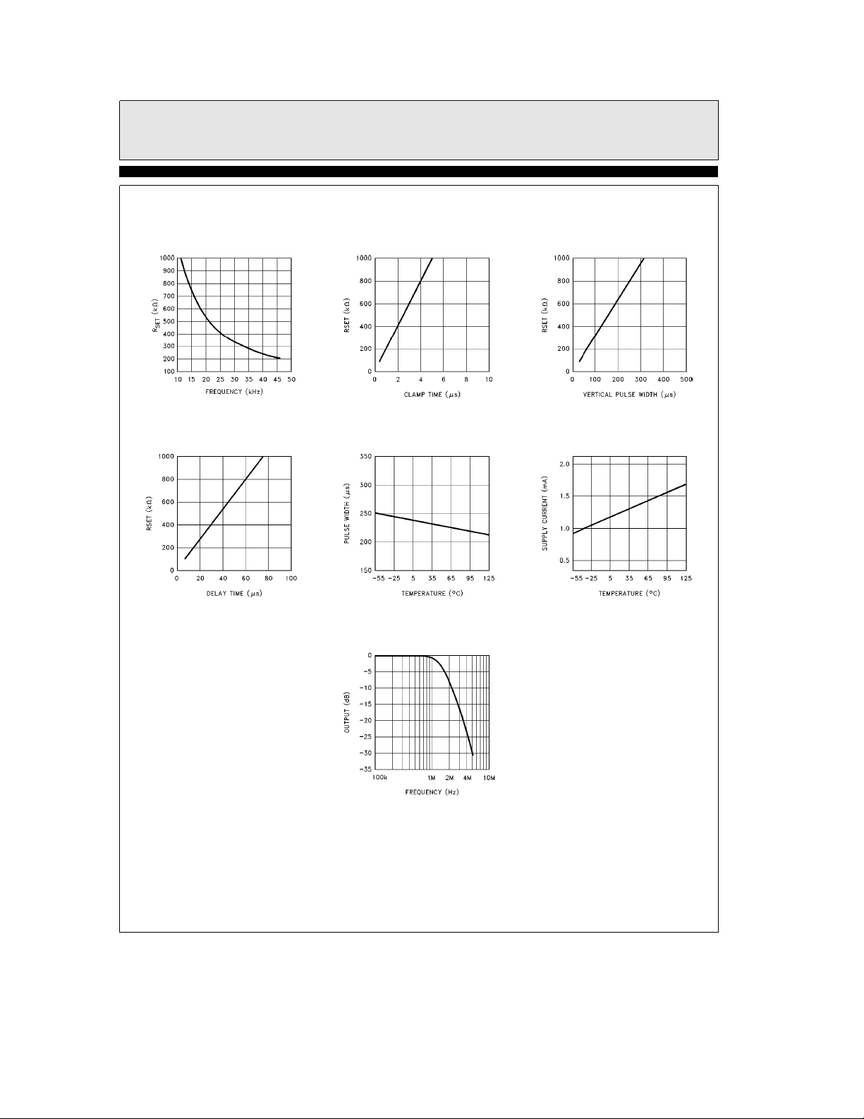
Typical Performance Characteristics
RSET vs Horizontal
Frequency
Vertical Default Delay
Time vs RSET
Back Porch Clamp
On Time vs RSET
Vertical Pulse Width
vs Temperature
e
Input Signal
EL4581 Filter Characteristic
Constant Delay 240 ns
300 mV
P-P
Vertical Pulse Width
vs RSET
Supply Current
vs Temperature
4581– 2
4
Page 5

Timing Diagrams
EL4581C
Sync Separator, 50% Slice, S-H, Filter
Notes:
b. The composite sync output reproduces all the video input sync pulses, with a propagation delay.
c. Vertical sync leading edge is coincident with the first vertical serration pulse leading edge, with a propagation delay.
d. Odd-even output is low for even field, and high for odd field.
e. Back porch goes low for a fixed pulse width on the trailing edge of video input sync pulses. Note that for serration pulses
during vertical, the back porch starts on the rising edge of the serration pulse (with propagation delay).
Figure 1
5
4581– 3
Page 6

EL4581C
Sync Separator, 50% Slice, S-H, Filter
Figure 2
Figure 3
6
4581– 5
4581– 6
Page 7

EL4581C
Sync Separator, 50% Slice, S-H, Filter
Figure 4. Standard (NTSC Input) H. Sync Detail
7
4581– 7
Page 8

EL4581C
Sync Separator, 50% Slice, S-H, Filter
Description of Operation
A simplified block schematic is shown in Figure
2. The following description is intended to provide the user with sufficient information to be
able to understand the effects that the external
components and signal conditions have on the
outputs of the integrated circuit.
The video signal is AC coupled to pin 2 via the
capacitor C
A1 will prevent the input signal on pin 2 going
any more negative than 1.5V, the value of reference voltage V
negative part of the video waveform, will be
clamped at 1.5V. The current source I
ly 10 mA, charges the coupling capacitor during
the remaining portion of the H line, approximately 58 ms for a 15.75 kHz timebase. From
I
teC#V, the video time-constant can be
#
calculated. It is important to note that the charge
taken from the capacitor during video must be
replaced during the sync tip time, which is much
shorter, (ratio of x 12.5). The corresponding current to restore the charge during sync will therefore be an order of magnitude higher, and any
resistance in series with C
crushing. For this reason, the internal series resistance has been minimized and external high
resistance values in series with the input coupling capacitor should be avoided. The user can
exercise some control over the value of the input
time constant by introducing an external pull-up
resistance from pin 2 to the 5V supply. The maximum voltage across the resistance will be V
less 1.5V, for black level. For a net discharge current greater than zero, the resistance should be
greater than 450k. This will have the effect of
increasing the time constant and reducing the degree of picture tilt. The current source I
tracks reference current I
with scan rate adjustment, as explained later.
The signal is processed through an active 3 pole
filter (F1) designed for minimum ripple with constant phase delay. The filter attenuates the color
burst by 24 dB and eliminates fast transient
spikes without sync crushing. An external filter
is not necessary. The filter also amplifies the
, nominally 0.1 mF. The clamp circuit
1
. Thus the sync tip, the most
R1
, nominal-
1
will cause sync tip
I
directly
and thus increases
TR
1
DD
video signal by 6 dB to improve the detection
accuracy. Note that the filter cut-off frequency is
a function of RSET through I
tional to I
OT
.
Internal reference voltages (block V
and is propor-
OT
REF
) with
high immunity to supply voltage variation are
derived on the chip. Reference V
with op-amp
R4
A2 forces pin 6 to a reference voltage of 1.7V
nominal. Consequently, it can be seen that the
external resistance RSET will determine the value of the reference current I
. The internal re-
TR
sistance R3 is only about 6 kX, much less than
RSET. All the internal timing functions on the
chip are referenced to I
and have excellent
TR
supply voltage rejection.
Comparator C2 on the input to the sample and
hold block (S/H) compares the leading and trailing edges of the sync. pulse with a threshold voltage V
the clamp voltage V
which is referenced at a fixed level above
R2
. The output of C2 initiates
R1
the timing one-shots for gating the sample and
hold circuits. The sample of the sync tip is delayed by 0.8 ms to enable the actual sample of
2 ms to be taken on the optimum section of the
sync. pulse tip. The acquisition time of the circuit
is about three horizontal lines. The double poly
CMOS technology enables long time constants to
be achieved with small high quality on-chip capacitors. The back porch voltage is similarly derived from the trailing edge of sync, which also
serves to cut off the tip sample if the gate time
exceeds the tip period. Note that the sample and
hold gating times will track RSET through I
OT
The 50% level of the sync tip is derived, through
the resistor divider R1 and R2, from the sample
and held voltages V
and VBP, and applied to
TIP
the plus input of comparator C1. This comparator has built in hysteresis to avoid false triggering. The output of C2 is a digital 5V signal which
feeds the C/S ouput buffer B1 and the other internal circuit blocks, the vertical, back porch and
odd/even functions.
The vertical circuit senses the C/S edges and initiates an integrator which is reset by the shorter
horizontal sync pulses but times out the longer
.
8
Page 9

EL4581C
Sync Separator, 50% Slice, S-H, Filter
Description of Operation
vertical sync. pulse widths. The internal timing
circuits are referenced to I
out period being inversely proportional to the
timing current. The vertical output pulse is started on the first serration pulse in the vertical interval and is then self-timed out. In the absense
of a serration pulse, an internal timer will default
the start of vertical.
The back porch is triggered from the sync tip
trailing edge and initiates a one-shot pulse. The
period of this pulse is again a function of I
will therefore track the scan rate set by RSET.
OT
Ð Contd.
and VR3, the time-
and
OT
Block Diagram
The odd/even circuit (O/E) comprises of flip
flops which track the relationship of the horizontal pulses to the leading edge of the vertical output, and will switch on every field at the start of
vertical. Pin 7 is high during the odd field.
Loss of video signal can be detected by monitoring the C/S output. The 50% level of the previous video signal will remain held on the S/H capacitors after the input video signal has gone and
the input on pin 2 has defaulted to the clamp
voltage. Consequently the C/S output will remain low longer than the normal vertical pulse
period. An external timing circuit could be used
to detect this condition.
*Note: RSET must be a 1% resistor.
Figure 5
4581– 4
9
Page 10

BLANK
10
Page 11

BLANK
11
Page 12

EL4581C
Sync Separator, 50% Slice, S-H, Filter
EL4581CJanuary 1996 Rev B
General Disclaimer
Specifications contained in this data sheet are in effect as of the publication date shown. Elantec, Inc. reserves the right to make changes
in the circuitry or specifications contained herein at any time without notice. Elantec, Inc. assumes no responsibility for the use of any
circuits described herein and makes no representations that they are free from patent infringement.
WARNING Ð Life Support Policy
Elantec, Inc. products are not authorized for and should not be
used within Life Support Systems without the specific written
consent of Elantec, Inc. Life Support systems are equipment in-
Elantec, Inc.
1996 Tarob Court
Milpitas, CA 95035
Telephone: (408) 945-1323
(800) 333-6314
Fax: (408) 945-9305
European Office: 44-71-482-4596
tended to support or sustain life and whose failure to perform
when properly used in accordance with instructions provided can
be reasonably expected to result in significant personal injury or
death. Users contemplating application of Elantec, Inc. products
in Life Support Systems are requested to contact Elantec, Inc.
factory headquarters to establish suitable terms & conditions for
these applications. Elantec, Inc.’s warranty is limited to replacement of defective components and does not cover injury to persons or property or other consequential damages.
Printed in U.S.A.12
 Loading...