

Page 1
EL4501C - Preliminary
Vi deo Front End
EL4501C - Preliminary
Features
• DC restore and sync s e parator
• Wideband (100MHz) DC restore
• Advanced sync separator
• Programmable data slicer
• Single 5 volt operation
• Differential Gain = 0.1%
• Differential Phase = 0.1°
• Low power (<75 mW)
Applications
• Video Capture & Editing
• Video Projectors
• Set Top Boxes
• Security Video
• Embedded data recovery
Ordering Information
Part No. Temp. Range Package Outline #
EL4501CS -40°C to +85°C 24-Pin SOIC MDP0027 EL4501CU -40°C to +85°C 24-Pin QSOP MDP0031
General Description
The EL4501C Video Front End (VFE) is an in tegrated soluti on that
provides the key analog signal conditioning functions for analog video
signals. It forms the front end interface for either an analog or analog/digital video syst em. The VFE contain s a high bandwidth DC
Restore, a sophistica ted Sync Se para tor, and a Data Sl icer for e mbedded data recovery.
The VFE will perform the restoration of the DC reference level
(blanking level) and the extraction of all of the necessary timing signals needed for synchronization and control. The sync separator is
designed for very good nois e im mun ity by incor pora ting a sign al q ualification scheme and internal brick wall filter. A data slicer is also
included to help decode data embedded in the active video or VBI
areas of the signal.
The VFE operates from a single 5 volt supply and is available in a
small 24 pin QSOP pac kag e tha t ta kes on ly 0.0 8in
2
(54mm
2
) of board
area, as well as a standard 24 pin SOIC.
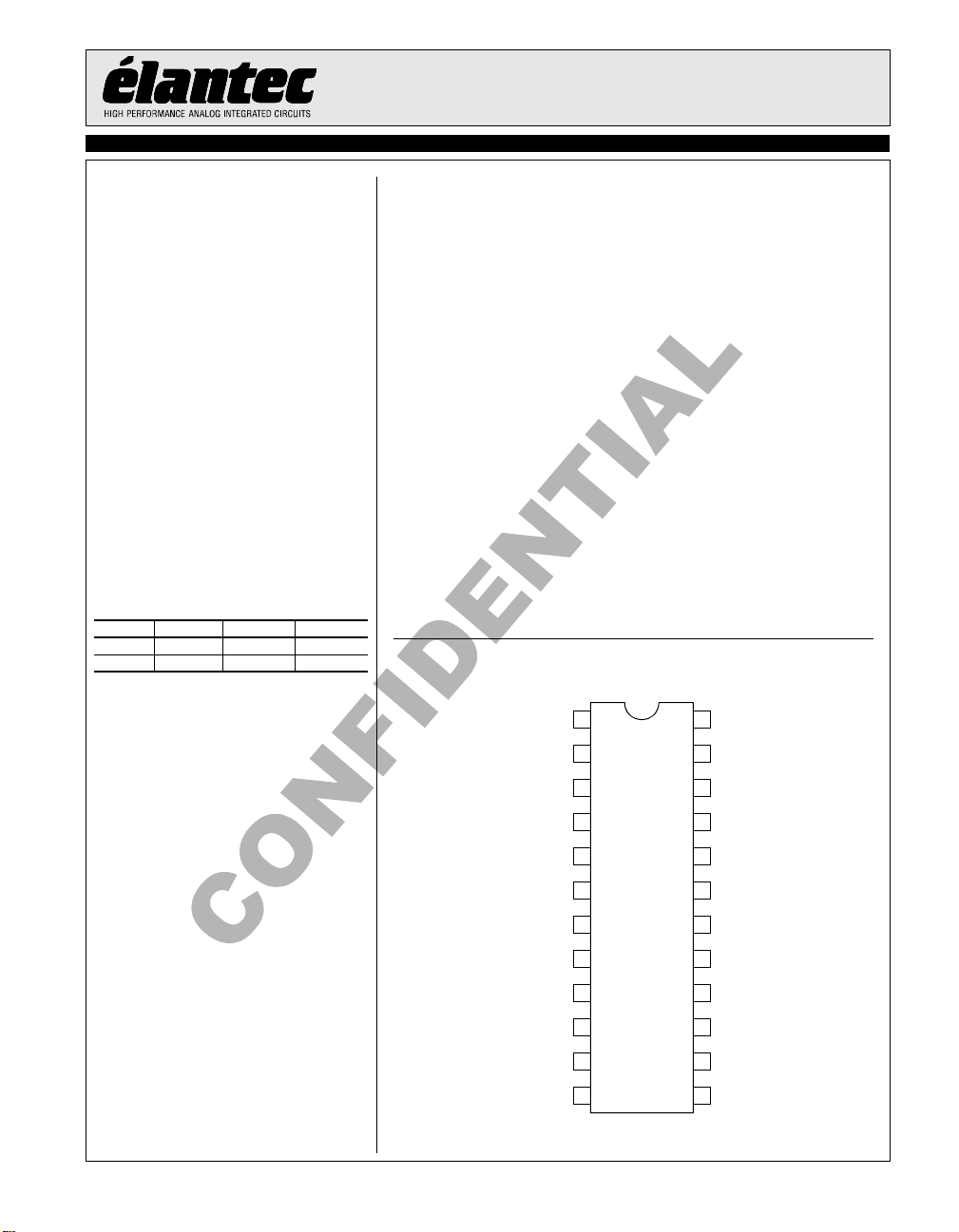
Connection Diagram
1
VIDEO_OUTVFB
24
© 2000 Elantec Semiconductor, Inc.
VIDEO_IN
DS_MODE
DS_ENAB
GND
GNDD
RFREQ
FSEL
SYNC_IN
LOS
COMPOSITE
HORIZONTAL
2
3
4
5
6
7
8
9
10
11
12
DS_OUT
23
DS_REF
22
REF_IN
21
REF_OUT
20
VS
19
VSD
18
SYNC_AMP
17
NC
16
BACK_PORCH
15
ODD/EVEN
14
VERTICAL
13
September 7, 2000
Page 2
EL4501C - Preliminary
Video Front End
Absolute Maximum Ratings (T
Values beyond absolute maximum ratings can cause the device to be prematurely damaged. Absolute maximum ratings are stress ratings only and
functional device operation is not implied.
Supply Voltage (V
EL4501C - Preliminary
Input Voltage GND - 0.3V, V
to GND) +6V
S
= 25°C)
A
+0.3V
S
Storage Temperature Range -65°C to +150°C
Ambient Operating Temperature -40°C to +85°C
Operating Junction Temperature 125°C
Power Dissipation See Curves
Important Note:
All parameters having Min/Max specifications are guaranteed. Typ values are for information purposes only. Unless otherwise noted, all tests are at the
specified temperature and are pulsed tests, therefore: T
= TC = TA.
J
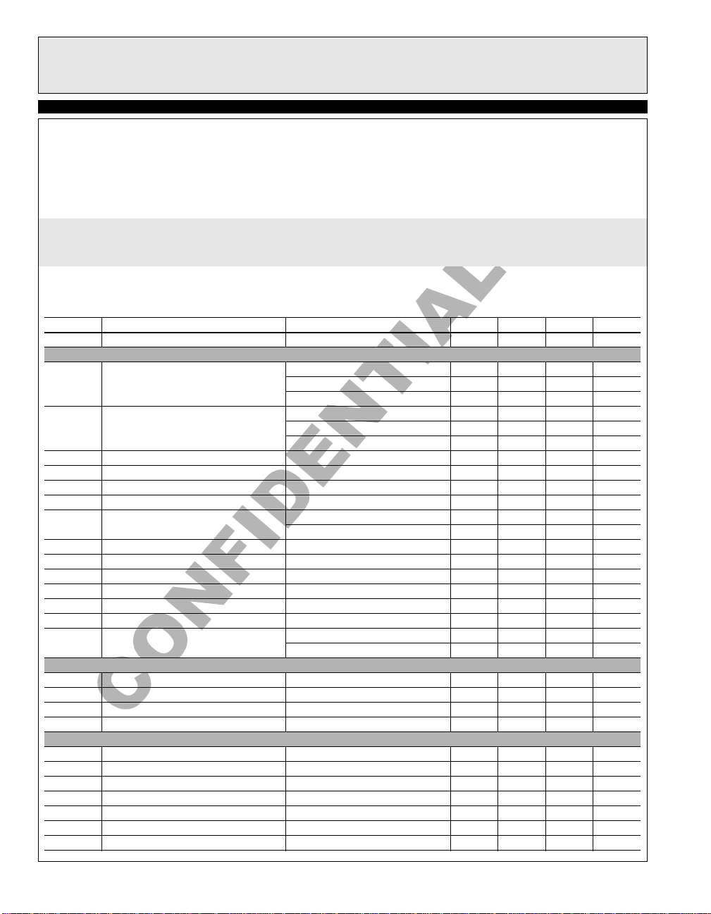
Electrical Characteristics
VS = +5V, GND = 0V, TA = 25°C, Input Video = 1V
Parameter Description Conditions Min Typ Max Unit
I
S
Supply Current No Load, V
Video Amplifier Section
V
OP
V
ON
+I
OUT
-I
OUT
dG Differential Gain Error
dP Differential Phase Error
Positive Output V oltage Swing RL = 150Ω to V
Negative Output V oltage Swing RL = 150Ω to V
Positive Output Current RL = 10Ω to V
Negative Output Current RL = 10Ω to V
[1]
[1]
BW Bandwidth -3dB, G = 1, R
BW1 Bandwidth +/-0.1dB, G = 2, R
SR Slew Rate 25% to 75%, 3.5V
V
RL
Ref Level Range 03.5V
ts Settling Time to 0.1%, V
R
IN
C
IN
A
VOL
Input Resistance (VIDEO_IN) 90 115 140 kΩ
Input Capacitance (VIDEO_IN) 1.5 pF
Open Loop Voltage Gain RL = no load, V
DC Restore Section
CMIR Common Mode Input Range (REF_IN) CMRR ≥ TBD dB 0 3.5 V
V
OS
TCV
I
B
Input Offset Voltage DC restored -20 +20 mV
Input Offset Voltage Temperature Coefficient 10 µV/°C
OS
Input Bias Current (REF_IN) VCM = 0V to 3.5V 1 100 nA
Data Slicer Section
I
I
V
V
V
V
I
IH
IL
IH
IL
OH
OL
OUT
Input High Current (DS_MODE & DS_ENAB) VIH = 5V 4 6 µA
Input Low Current (DS_MODE & DS_ENAB) VIL = 0V 1 100 nA
Input High Voltage (DS_MODE & DS_ENAB) 4.5 V
Input Low Voltage (DS_MODE & DS_ENAB) 0.5 V
Output High V oltage (DS_OUT) I
Output Low Voltage (DS_OUT) I
Short Circuit Current (DS_OUT) RL = 10Ω to 2.5V 15 20 mA
unless otherwise specified.
P-P
R
= 150Ω to GND 4.20 4.60 V
L
R
= 1k to V
L
R
= 150Ω to GND 0 V
L
R
= 1k to V
L
Standard NTSC test, AV = 2, RL = 150Ω 0.1 %
Standard NTSC test, AV = 2, RL = 150Ω 0.1 °
-3dB, G = 1, R
R
= 150Ω to GND, V
L
= -1mA 4.75 4.9 V
OUT
= 1mA 0.1 0.25 V
OUT
= 0V 20 mA
IN
S
/2
S
/2
S
/2
S
/2
S
/2
S
/2
L = 10kΩ to GND 100 MHz
L = 150Ω to GND 60 MHz
L = 150Ω to GND 8 MHz
, RL = 150Ω 150 200 V/µs
P-P
= 0V to 3V 35 ns
IN
= 0.5V to 3V 54 65 dB
OUT
= 0.5V to 3V 40 50 dB
OUT
4.70 4.85 V
4.95 4.97 V
0.15 0.30 V
0.03 0.05 V
60 80 120 mA
-50 -60 -80 mA
2
Page 3
EL4501C - Preliminary
Video Front End
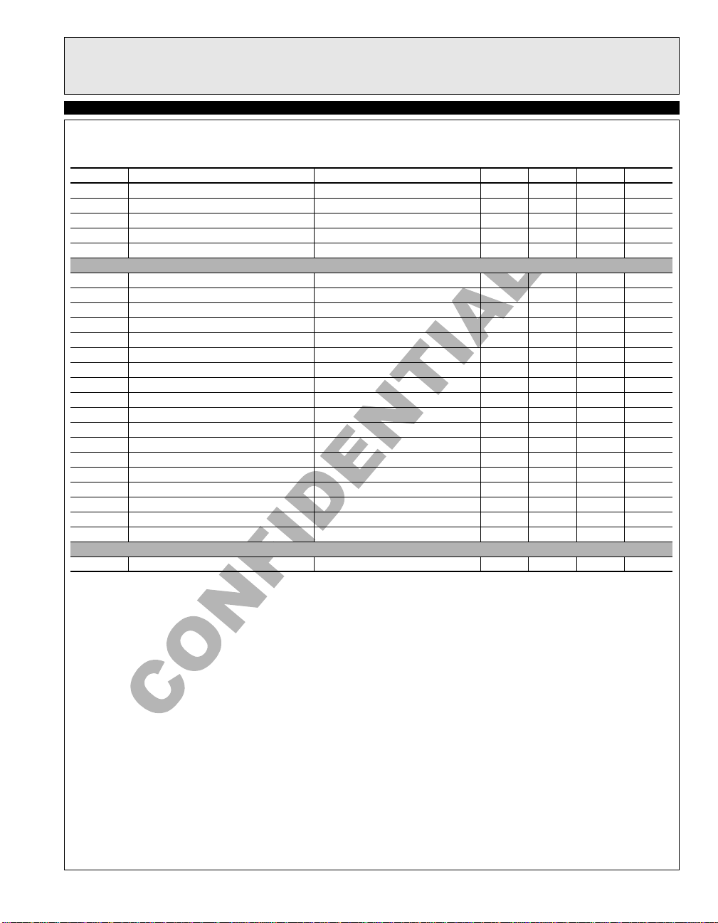
Electrical Characteristics
VS = +5V, GND = 0V, TA = 25°C, Input Video = 1V
Parameter Description Conditions Min Typ Max Unit
I
B
Input Bias Current (DS_REF) DS_REF = 0V & 5V -100 1 100 nA Vos Input Offset Voltage -20 +20 mV V
HYS
t
PD
t
R/F
Hysteresis 10 15 mV
Propagation Delay 50% to 50% 18 28 ns
Rise/Fall Time 10% to 90%, RL = 150k, CL = 5pF 1.2 1.8 ns
Sync Separator Section
V
OH
V
OL
V
THSRH
T
CD
T
CD
V
SR
R
INSR
V
RANGE
t
CD
t
BD
t
BW
t
HD
t
HW
t
VW
t
VDD
f
H
V
LOS
t
JIT
Output High V oltage I
Output Low V oltage I
Slicing Level 45 50 55 %
Composite Sync Delay With Filter TBD TBD
Composite Sync Delay Without Filter TBD TBD
Sync In Reference Level 1.5 V
Sync Reference Input Impedance 90 kΩ
Input Dynamic Range 0.5 2.0 Vp-p
Comp Sync Delay From 50% point of leading edge of sync 50 75 100 ns
Back Porch Delay From 50% point of trailing edge of sync 34 0 430 520 ns
Back Porch Width 2.7 3.0 3.3 µs
Horiz Sync Delay From 50% point of leading edge of sync 350 450 550 ns
Horiz Sync Width 3.7 4.7 5.7 µs
V ert Sync Width Serrations 185 195 205 µs
Vert Sync Default Delay No serrations 51 63.5 76 µs
Horiz Scan Rate R
LOS Detect Threshold Compared to Sync Tip Amplitude 72 mV
Output Jitter All sync separator outputs 5 ns
Reference Section
VREF Reference Output Voltage (REF_OUT) I
unless otherwise specified.
P-P
= -1.6mA 4.6 V
OH
= 1.6mA 0.4 V
OL
= xx to yy kΩ 15 130 kHz
FREQ
= +2mA to -0.5mA 1.2 1.3 1.4 V
OUT
EL4501C - Preliminary
3
Page 4

EL4501C - Preliminary
Video Front End
Typical Performance Curves
EL4501C - Preliminary
4
Page 5

Timing Diagrams
Fields One and Three (ODD)
Composite Signal
Composite Sync Output
Burst/Back Porch Output
Horizontal Sync Output
Vertical Sync Output
Odd/Even Output
EL4501C - Preliminary
EL4501C - Preliminary
Video Front End
Fields Two and Four (EVEN)
Composite Signal
Composite Sync Output
Burst/Back Porch Output
Horizontal Sync Output
Vertical Sync Output
Odd/Even Output
5
Page 6

EL4501C - Preliminary
Video Front End
Timing Diagrams (cont.)
EL4501C - Preliminary
Video In
Composite Sync Output
Burst/Back Porch Output
Horizontal Sync Output
Video In
Vertical Sync Output
ODD/EVEN
t
CD
t
HD
t<< t
CD
t
HW
tCD+2t
tCD+t
t
BD
t
BW
6
Page 7

EL4501C - Preliminary
Video Front End
Pin Description
Pin
Number Pin Name Pin Type Pin Description
1 VFB Input Connection for gain and feedback resistors, R
2 VIDEO_IN Input Input to DC restore amplifier. Input coupling capacitor connects from here to video source.
3 DS_MODE Input Sets the mode of the DS comparator. Logic high selects a standard logic output. Logic low selects an open
4 DS_ENAB Input Enables the output of the comparator. A logic high enables the comparator. A logic low tri-states it.
5 GND Input Analog ground.
6 GND
7R
8 FSEL Input Enable/ bypass internal brick wall filter. A logic high is used to enable the filter, a logic low to disable it.
9 SYNC_IN Input Input to the sync separator. Connects to the video source via a coupling capacitor, or to a color burst input filter.
10 LOS Output Loss of signal output. Goes high if no input video signal is detected.
11 COMPOSITE Output Composite sync output.
12 HORIZONTAL Output Horizontal sync output.
13 VERTICAL Output Vertical sync output.
14 ODD/EVEN Output Odd/Even field indicator output.
15 BACK_PORCH Output Back porch output.
17 SYNC_AMP Output Amplitude of sync tip. Can be used to control AGC circuit.
18 V
19 V
20 REF-OUT Output Voltage reference for use as blanking level in low cost system
21 REF_IN Input Dc voltage on this pin sets the DC restore voltage and output blanking level.
22 DS_REF Input Sets the slicing level or reference level for the comparator.
23 DS_OUT Output Output of the data slicing comparator. The output is either open drain/collector or standard symmetrical logic
24 VIDEO_OUT Output Output of DC restore amplifier.
D
FREQ
SD
S
Input Digital ground
Input Connection for bias resistor that sets the overall timing.
Input Digital power supply. Nominally +5V
Input Analog power supply. Nominally +5V.
drain/collector.
depending on the DS_MODE pin.
and RG.
F
EL4501C - Preliminary
7
Page 8

EL4501C - Preliminary
Video Front End
Block Diagram
EL4501C - Preliminary
Input video
VIDEO_IN
0.1uF
SYNC_IN
0.1uF
SYNC_AMP
V
S
LOS
R
FREQ
V
SD
+
-
LOS’
FilterFSEL
Sync Separator
GND
DS_REF
GND
D
DS_MODE
+
1.3V
DS_ENAB
DS_OUT
VIDEO_OUT
R
VFB
R
REF_IN
REF_OUT
BACK_PORCH
COMPOSITE
HORIZONTAL
VERTICAL
ODD/EVEN
F
G
+
-
+
-
–
8
Page 9

Description of Operation
The EL4501C incorporates the following functional
blocks:
• DC restore amplifier
• Advanced sync separator
• Data Slicer
Combined they pr ovid e t he key ana l og pr oc essing fun ctions for a number of video system applications. The
operation of each of these blocks is described below.
Sync Separa t or
The sync separator contained in the EL4501C has been
designed to be compatible with a wide range of video
signal standards, operating with horizontal line rates
from PAL/NTSC rates up to 150kHz. The sync separator
EL4501C - Preliminary
Video Front End
also includes a qualification scheme which rejects noise
pulses and other video arti facts. The h orizontal l ine rate
timing is controlled with the use of a resistor, R
The following outputs are available:
• Composite sync
• Horizontal sync
• Vertical sync
• Burst gate
• Odd/Even field identification
• Loss of signal detected
• Sync amplitude detected
FREQ
.
EL4501C - Preliminary
9
Page 10

EL4501C - Preliminary
Video Front End
EL4501C - Preliminary
General Disclaimer
Specifications contained in this data sheet are in effect as of the publicat ion date shown. Elantec, Inc. re serves the r ight to make changes in th e circuitry or specifications cont ained herein at a ny time without notice. Elantec , Inc. assumes no res ponsibili ty for t he us e of an y circuits descr ibed
herein and makes no representations that they are free from patent infringement.
WARNING - Life Support Policy
Elantec, Inc. products are not authorized for and should not be used
within Life Support Systems without the specific written consent of
Elantec, Inc. Life Support systems are equipment intend ed to sup-
Elantec Semiconductor, Inc.
675 Trade Zone Blvd.
Milpitas, CA 95035
Telephone: (408) 945-1323
(888) ELANTEC
Fax: (408) 945-9305
European Office: +44-118-977-6080
Japan Technical Center: +81-45-682 -5820
port or sustain life and whose failure to perform when properly used
in accordance with instructions provided can be reasonably
expected to result in significant personal injury or death. Users contemplating applicatio n of Elantec, Inc. P roducts in Li fe Support
Systems are requested to contact Elantec, Inc. factory headquarters
to establish suitable terms & conditions for these applications. Elantec, Inc. ’s warranty is limited to replacement of defective
components and does not cov er injury to persons or prop erty or
other consequential damages.
September 7, 2000
10
Printed in U.S.A.
 Loading...