

Page 1
EL4453C
Video Fader
EL4453C January 1995 Rev A
Features
# Complete two-input fader with
output amplifierÐuses no extra
components
# 80 MHz bandwidth
# Fast fade control speed
# Operates on
g
5V tog15V
supplies
l
#
60 dB attenuation@5 MHz
Applications
# Mixing two inputs
# Picture-in-picture
# Text overlay onto video
# General gain control
Ordering Information
Part No. Temp. Range Pkg. Outline
EL4453CNb40§Ctoa85§C 14-Pin P-DIP MDP0031
EL4453CSb40§Ctoa85§C 14-Lead SOIC MDP0027
General Description
The EL4453C is a complete fader subsystem. It variably blends
two inputs together for such applications as video picture-inpicture effects.
The EL4453C operates on
analog differential input range of
g
5V tog15V supplies and has an
g
2V. AC characteristics do
not change appreciably over the supply range.
The circuit has an operational temperature of
b
40§Ctoa85§C
and is packaged in 14-pin P-DIP and SO-14.
The EL4453C is fabricated with Elantec’s proprietary complementary bipolar process which gives excellent signal symmetry
and is free from latch up.
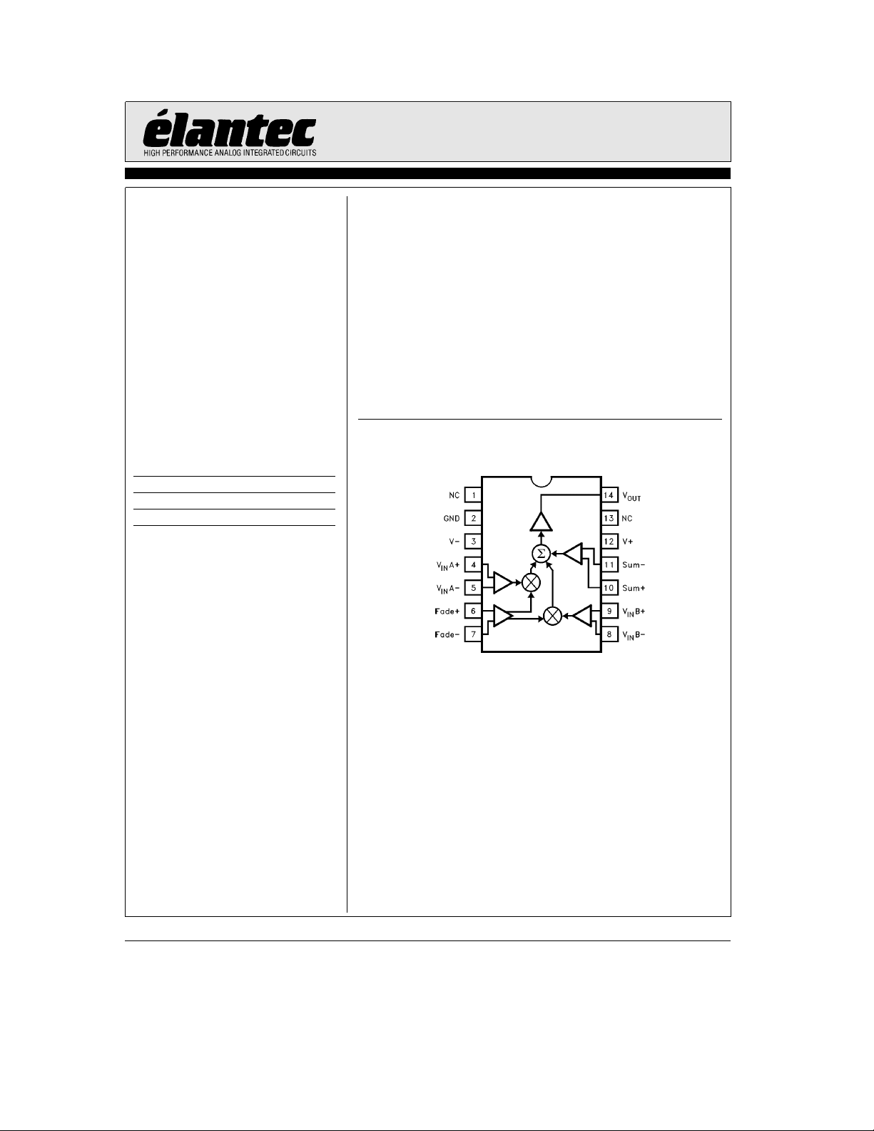
Connection Diagram
Ý
4453– 1
Note: All information contained in this data sheet has been carefully checked and is believed to be accurate as of the date of publication; however, this data sheet cannot be a ‘‘controlled document’’. Current revisions, if any, to these
specifications are maintained at the factory and are available upon your request. We recommend checking the revision level before finalization of your design documentation.
©
1995 Elantec, Inc.
Page 2

EL4453C
Video Fader
Absolute Maximum Ratings
a
V
V
S
V
IN
DV
Important Note:
All parameters having Min/Max specifications are guaranteed. The Test Level column indicates the specific device testing actually
performed during production and Quality inspection. Elantec performs most electrical tests using modern high-speed automatic test
equipment, specifically the LTX77 Series system. Unless otherwise noted, all tests are pulsed tests, therefore T
Test Level Test Procedure
Open-Loop DC Electrical Characteristics
Power Supplies atg5V, SumaeSumbe0, T
Parameter Description Min Typ Max
V
DIFF
V
CM
V
OS
V
FADE
V
FADE
I
B
I
OS
F
T
Positive Supply Voltage 16.5V
Vato VbSupply Voltage 33V
Voltage at any Input or Feedback Vato V
Difference between Pairs
IN
of Inputs or Feedback 6V
I 100% production tested and QA sample tested per QA test plan QCX0002.
II 100% production tested at T
III QA sample tested per QA test plan QCX0002.
IV Parameter is guaranteed (but not tested) by Design and Characterization Data.
V Parameter is typical value at T
T
MAX
and T
per QA test plan QCX0002.
MIN
VINA, VINB, or Sum Differential Input VoltageÐ Clipping 1.8 2.0 I V
Common-Mode Range (All Inputs; V
A or B Input Offset Voltage 25 I mV
, 100% Extrapolated Voltage for 100% Gain for VINA 0.9 1.05 1.2 I V
, 0% Extrapolated Voltage for 0% Gain for VINA
Input Bias Current (All Inputs) with all V
Input Offset Current between VINAaand VINAb, 0.2 4 I mA
Baand VINBb, Fadeaand Fadeb,
V
IN
and Sumaand Sum
VINA Signal Feedthrough, V
b
FADE
e
T
25§C
A
I
I
b
P
T
T
e
25§C and QA sample tested at T
A
e
25§C for information purposes only.
A
e
25§C
A
e
0) V
DIFF
e
0 9 20 I mA
IN
eb
1.5V
Current into any Input, or Feedback Pin 4 mA
IN
Output Current 30 mA
OUT
Maximum Power Dissipation See Curves
D
Operating Temperature Range
A
Storage Temperature Range
S
e
25§C,
A
b
b
60§Ctoa150§C
e
e
T
J
C
Level
0.2% Nonlinearity 0.7 V V
e
g
5V
S
e
g
15V
V
S
g
2.5g2.8 I V
g
12.5g12.8 I V
b
1.2b1.15b0.9 I V
b
100b60 I dB
40§Ctoa85§C
TA.
Test
Units
NL A or B Input Nonlinearity, VINbetweena1V andb1V, VINAorVINB 0.2 0.5 I %
Sum Input 0.5 V %
RIN, Signal Input Resistance, A, B, or Sum Input 230 V kX
RIN, Fade Input Resistance, Fade Input 120 V kX
CMRR Common-Mode Rejection Ratio, VINAorVINB7080IdB
PSRR Power Supply Rejection Ratio 50 70 I dB
E
G
V
O
I
SC
I
S
Gain Error, V
Output Voltage Swing V
e
0, V
(V
IN
e
1.5V, VINAorVINB
FADE
Varied) V
REF
Sum Input
e
g
S
e
g
S
5V
15V
Output Short-Circuit Current 40 85 I mA
e
Supply Current, V
g
15V 17 21 I mA
S
b
2
b
4
g
2.5g2.8 I V
g
12.5g12.8 I V
a
2I %
a
4I %
TDis 4.3in
2
Page 3
EL4453C
Video Fader
Closed-Loop AC Electrical Characteristics
Power supplies atg12V, T
Parameter Description Min Typ Max
BW,b3dB
BW,g0.1 dB 0.1 dB Flatness Bandwidth, VINAorVINB 9 V MHz
Peaking Frequency Response Peaking 1.0 V dB
BW, Fade
SR Slew Rate, V
V
N
F
T
dG Differential Gain Error, V
di Differential Phase Error, V
b
b
Input-Referred Noise Voltage Density 160 V nV/Hz
Feedthrough of Faded-Out Channel, Fe3.58 MHz
e
25§C, R
A
3 dB Small-Signal Bandwidth, VINAorVINB 80 V MHz
3 dB Small-Signal Bandwidth, Fade Input 80 V MHz
OUT
e
500X,C
L
betweenb2V anda2V TBD 380 I V/ms
OFFSET
OFFSET
e
15 pF, V
L
from 0 tog0.714V, Fade at 100%
from 0 tog0.71V, Fade at 100%
e
FADE
1.5V, SumaeSumbe0
V
AorVINB 0.05 V %
IN
Sum Input 0.35 V %
V
AorVINB 0.05 V (§)
IN
Sum Input 0.1 V (
Test
Level
b
63 V dB
Units
Test Circuit
)
§
TDis 2.5in
Note: For typical performance curves Sum
otherwise noted.
ae
Sum
be
0, R
e
F
3
0X,R
G
e %
,V
FADE
ea
1.5V, and C
4453– 2
L
e
15 pF, unless
Page 4

EL4453C
Video Fader
Typical Performance Curves
Frequency Response
Frequency Response for
Various Loads, V
b
3 dB Bandwidth and Peaking
vs Supply Voltage
e
S
Frequency Response vs Gain
4453– 3
g
5V
4453– 6
Frequency Response for
Various Loads, V
b
3 dB Bandwidth and Peaking
vs Die Temperature
e
S
g
15V
4453– 4
4453– 7
4453– 9
4453– 10
4
Page 5

EL4453C
Video Fader
Typical Performance Curves
Frequency Response for
Different Gains, V
VINDifferential Gain
and Phase Error vs Gain
e
g
5V
S
4453– 5
Ð Contd.
Input Common-Mode Rejection
Ratio vs Frequency
4453– 8
Input Voltage and Current
Noise vs Frequency
VINDifferential Gain Error
vs Input Offset Voltage
for Gain
e
100%, 75%, 50% and 25%
4453– 11
VINDifferential Phase Error
vs Input Offset Voltage for Gain
100%, 75%, 50% and 25%. V
e
S
4453– 14
e
g
5V
4453– 16
VINDifferential Phase Error
vs Input Offset Voltage for Gain
100%, 75%, 50% and 25%. V
S
4453– 15
e
e
g
12V
4453– 17
5
Page 6

EL4453C
Video Fader
Typical Performance Curves
Nonlinearity vs VINSignal Span
Slew Rate vs Supply Voltage
Ð Contd.
4453– 12
Nonlinearity vs Sum Signal Span
4453– 13
Slew Rate vs Die Temperature
VINA Gain vs V
FADE
4453– 18
4453– 20
4453– 19
Frequency Response of Fade Input
4453– 21
6
Page 7

EL4453C
Video Fader
Typical Performance Curves
Transient Response of Fade Input
Constant Signal into V
VINA Transient Response for Various Gains
A
IN
Ð Contd.
4453– 22
Overdrive Recovery Glitch from
, No Input Signal
V
FADE
Cross-Fade Balance with VINAeVINBe0
4453– 23
Supply Current vs Supply Voltage
4453– 24
4453– 26
4453– 25
Supply Current vs Die Temperature
4453– 27
7
Page 8

EL4453C
Video Fader
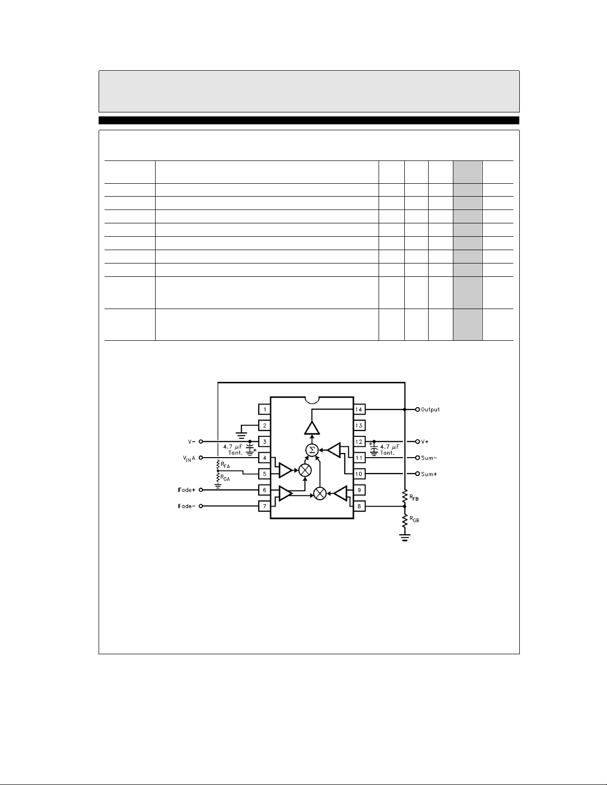
Applications Information
The EL4453C is a complete two-quadrant fader/
gain control with 80 MHz bandwidth. It has four
sets of inputs; a differential signal input V
differential signal input V
B, a differential
IN
IN
A, a
fade-controlling input V
ferential input Sum which can be used to add in a
third input at full gain. This is the general connection of the EL4453C:
, and another dif-
FADE
4453– 28
8
Page 9

EL4453C
Video Fader
Applications Information
The gain of the feedback dividers are H
H
, and 0sHs1. The transfer function of the
B
Ð Contd.
A
and
part is
V
OUT
with
a
c
e
[
A
((V
O
c
((VINBa)–H
a
(V
FADE
b
1s(V
FADE
Aa)–H
IN
(1a(V
c
B
))/2a(Suma)–(Sumb))],
b
a
FADE
V
OUT
)–(V
c
V
A
)b(V
a
)c(1b(V
FADE
OUT
b
)
FADE
s
)
b
FADE
a
1 nu-
))/2
a
merically.
A
is the open-loop gain of the amplifier, and is
O
about 600. The large value of A
FADE
c
V
A
b
c
)c(1a(V
OUT
))/2a((VINBa)–H
(1b(V
FADE
a
(Suma)–(Sumb))x0.
((V
Aa)–H
IN
–(V
O
)a(V
a
drives
FADE
FADE
)
a
c
V
B
OUT
))/2
b
Rearranging and substituting
OUT
FcH
Where Fe(1a(V
e(1b
F
(V
A
FADE
FADE
a
FcH
)–(V
a
)a(V
a
Sum
FADE
e
(Suma)–(Sumb)
B
FADE
))/2,
b
))/2, and
b
FcVINAaFcVINBaSum
e
V
In the above equations, F represents the fade
amount, with F
but 0% for V
V
A but 100% to VINB. F is 1bF, the comple-
IN
ment of the fade gain. When F
e
1 giving 100% gain on VINA
B; Fe0 giving 0% gain for
IN
e
1,
VINAaSum
e
V
OUT
H
A
The EL4453C is stable for a direct connection between V
gain of
and VINAbor VINBb, yielding a
OUT
a
1. The feedback divider may be used for
higher output gain, although with the traditional
loss of bandwidth. It is important to keep the
feedback dividers’ impedances low so that stray
capacitance does not diminish the feedback loop’s
phase margin. The pole caused by the parallel im-
)
pedance of the feedback resistors and stray capacitance should be at least 150 MHz; typical
strays of 3 pF thus require a feedback impedance
of 360X or less. Alternatively, a small capacitor
across R
can be used to create more of a fre-
F
quency-compensated divider. The value of the capacitor should scale with the parasitic capacitance at the FB input. It is also practical to place
small capacitors across both the feedback resistors (whose values maintain the desired gain) to
)
swamp out parasitics. For instance, two 10 pF
capacitors across equal divider resistors for a gain
of two will dominate parasitic effects and allow a
higher divider resistance. Either input channel
can be set up for inverting gain using traditional
feedback resistor connections.
At 100% gain, an input stage operates just like
an op-amp’s input, and the gain error is very low,
around
b
0.2%. Furthermore, nonlinearities are
vastly improved since the gain core sees only
small error signals, not full inputs. Unfortunately, distortions increase at lower fade gains for a
given input channel.
The Sum pins can be used to inject an additional
input signal, but it is not as linear as the V
paths. The gain error is also not as good as the
main inputs, being about 1%. Both sum pins
should be grounded if they are not to be used.
IN
and the amplifier passes VINA and Sum with a
gain of 1/H
. Similarly, for Fe0
A
VINBaSum
e
V
OUT
H
B
and the gains vary linearly between fade extremes.
9
Page 10

EL4453C
Video Fader
Fade-Control Characteristics
The quantity V
bounded as
b
1sV
externally applied voltages often exceed this
range. Actually, the gain transfer function
around
b
1V anda1V is ‘‘soft’’, that is, the gain
does not clip abruptly below the 0%-V
age or above the 100% – V
drive of 0.3V must be applied to V
truly 0% or 100%. Because the 0%
V
levels cannot be precisely determined,
FADE
they are extrapolated from two points measured
inside the slope of the gain transfer curve. Generally, an applied V
will assure the full span of numerical
FADE
s
1 and 0sFs1.
s
V
The fade control has a small-signal bandwidth
equal to the V
IN
load recovery resolves in about 20 ns.
in the above equations is
FADE
FADE
s
FADE
1, even though the
FADE
level. An over-
FADE
FADE
e
to obtain
or 100%-
range ofb1.5V toa1.5V
channel bandwidth, and over-
volt-
b
Input Connections
The input transistors can be driven from resistive
and capacitive sources, but are capable of oscillation when presented with an inductive input. It
takes about 80 nH of series inductance to make
the inputs actually oscillate, equivalent to four
inches of unshielded wiring or about six inches of
unterminated input transmission line. The oscillation has a characteristic frequency of 500 MHz.
Often placing one’s finger (via a metal probe) or
an oscilloscope probe on the input will kill the
oscillation. Normal high frequency construction
obviates any such problems, where the input
source is reasonably close to the fader input. If
this is not possible, one can insert series resistors
of around 51X to de-Q the inputs.
Signal Amplitudes
Signal input common-mode voltage must be between (V
linearity. Additionally, the differential voltage on
any input stage must be limited to
vent damage. The differential signal range is
g
stantially constant with temperature.
b)a
2.5V and (Va)b2.5V to ensure
g
6V to pre-
2V in the EL4453C. The input range is sub-
The Ground Pin
The ground pin draws only 6 mA maximum DC
current, and may be biased anywhere between
b)a
(V
2.5V and (Va)b3.5V. The ground pin
is connected to the IC’s substrate and frequency
compensation components. It serves as a shield
within the IC and enhances input stage CMRR
and channel-to-channel isolation over frequency,
and if connected to a potential other than
ground, it must be bypassed.
Power Supplies
The EL4453C works well on any supplies from
g
1
3V tog15V. The supplies may be of different
voltages as long as the requirements of the GND
pin are observed (see the Ground Pin section for
a discussion). The supplies should be bypassed
close to the device with short leads. 4.7 mF tantalum capacitors are very good, and no smaller bypasses need be placed in parallel. Capacitors as
small as 0.01 mF can be used if small load currents flow.
Singe-polarity supplies, such as
a
12V witha5V
can be used, where the ground pin is connected to
a
5V and Vbto ground. The inputs and outputs
will have to have their levels shifted above
ground to accommodate the lack of negative supply.
The dissipation of the fader increases with power
supply voltage, and this must be compatible with
the package chosen. This is a close estimate for
the dissipation of a circuit:
e
P
2cVS, maxcV
D
a
b
(V
S
VO)cVO/R
S
where IS, max is the maximum supply current
V
is thegsupply voltage
S
(assumed equal)
V
is the output voltage
O
R
is the parallel of all resistors
PAR
loading the output
PAR
10
Page 11

Power Supplies
For instance, the EL4453C draws a maximum of
21 mA. With light loading, R
dissipation with
maximum supply voltage that the device can run
on for a given P
V
, maxe(P
S
The maximum dissipation a package can offer is
P
, maxe(TD, maxbTA, max)/i
D
where TD, max is the maximum die tempera-
ture, 150
optimum electrical performace
T
for commercial and 85
range
i
mounted package, obtained from datasheet dissipation curves
The more difficult case is the SO-14 package.
With a maximum die temperature of 150
maximum ambient temperature of 70
temperature rise and package thermal resistance
of 110
/W gives a dissipation of 636 mW at 85§C.
§
a
D
, max is the ambient temperature, 70§C
A
is the thermal resistance of the
JA
Ð Contd.
%
a
VO/R
JA
C, the 80§C
§
and the
PAR
C and a
§
x
PAR
PAR
)/(2I
S
C for industrial
§
g
5V supplies is 210 mW. The
and the other parameters is
D
2
V
/R
O
C for reliability, less to retain
§
)
EL4453C
Video Fader
g
This allows
temperature range, but higher ambient temperature or output loading may require lower supply
voltages.
Output Loading
The output stage of the EL4453C is very powerful. It typically can source 80 mA and sink
120 mA. Of course, this is too much current to
sustain and the part will eventually be destroyed
by excessive dissipation or by metal traces on the
die opening. The metal traces are completely reliable while delivering the 30 mA continuous output given in the Absolute Maximum Ratings table in this data sheet, or higher purely transient
currents.
Gain changes only 0.2% from no load to 100X
load. Heavy resistive loading will degrade frequency response and video distortion for loads
k
100X.
Capacitive loads will cause peaking in the frequency response. If capacitive loads must be driven, a small-valued series resistor can be used to
isolate it. 12X to 51X should suffice. A 22X series
resistor will limit peaking to 2.5 dB with even a
220 pF load.
15V operation over the commercial
11
Page 12

EL4453C
Video Fader
EL4453CJanuary 1995 Rev A
General Disclaimer
Specifications contained in this data sheet are in effect as of the publication date shown. Elantec, Inc. reserves the right to make changes
in the circuitry or specifications contained herein at any time without notice. Elantec, Inc. assumes no responsibility for the use of any
circuits described herein and makes no representations that they are free from patent infringement.
WARNING Ð Life Support Policy
Elantec, Inc. products are not authorized for and should not be
used within Life Support Systems without the specific written
consent of Elantec, Inc. Life Support systems are equipment in-
Elantec, Inc.
1996 Tarob Court
Milpitas, CA 95035
Telephone: (408) 945-1323
(800) 333-6314
Fax: (408) 945-9305
European Office: 44-71-482-4596
tended to support or sustain life and whose failure to perform
when properly used in accordance with instructions provided can
be reasonably expected to result in significant personal injury or
death. Users contemplating application of Elantec, Inc. products
in Life Support Systems are requested to contact Elantec, Inc.
factory headquarters to establish suitable terms & conditions for
these applications. Elantec, Inc.’s warranty is limited to replacement of defective components and does not cover injury to persons or property or other consequential damages.
Printed in U.S.A.12
 Loading...