

Page 1
EL4452C
Wideband Variable-Gain Amplifier with Gain of 10
EL4452C December 1994 Rev A
Features
# Complete variable-gain amplifier
complete with output amplifier
# Compensated for Gain
t
10
# 50 MHz signal bandwidth
# 50 MHz gain-control bandwidth
# Low 29 nV/
# Operates on
S
Hz input noise
g
5V tog15V
supplies
# All inputs are differential
l
#
70 dB attenuation@5 MHz
Applications
# AGC variable-gain amplifier
# IF amplifier
# Transducer amplifier
Ordering Information
Part No. Temp. Range Package Outline
EL4452CNb40§Ctoa85§C 14-pin P-DIP MDP0031
EL4452CS
b
40§Ctoa85§C 14-lead SO MDP0027
General Description
The EL4452 is a complete variable-gain circuit. It offers wide
bandwidth and excellent linearity, while including a powerful
output voltage amplifier, drawing modest current. The higher
gain and lower input noise makes the EL4452 ideal for use in
AGC systems.
The EL4452 operates on
range of
g
0.5V. AC characteristics do not change appreciably
g
5V tog15V and has an analog input
over the supply range.
The circuit has an operational temperature of
b
40§Ctoa85§C
and is packaged in 14-pin P-DIP and SO-14.
The EL4452 is fabricated with Elantec’s proprietary complementary bipolar process which gives excellent signal symmetry
and is very rugged.
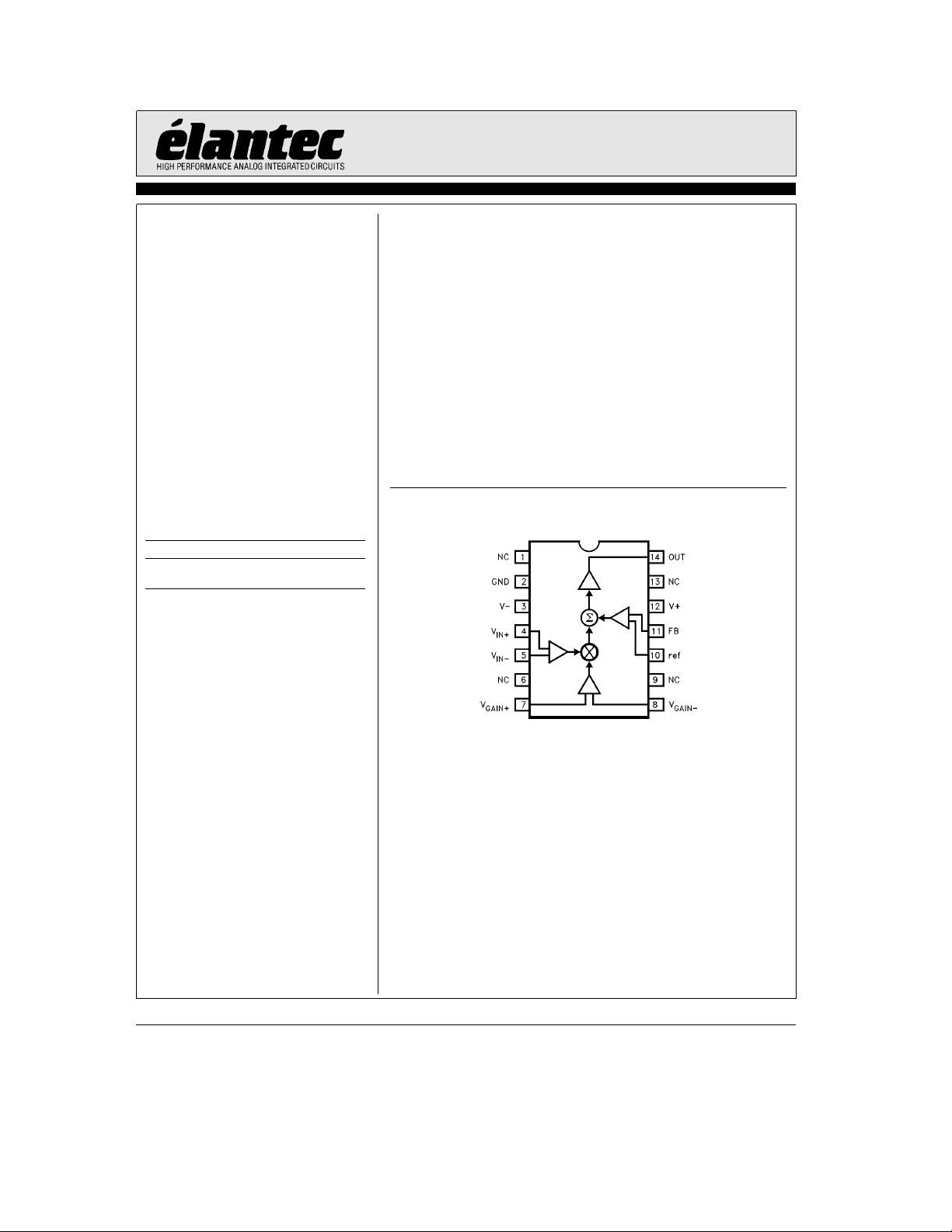
Connection Diagram
Ý
4452– 1
Note: All information contained in this data sheet has been carefully checked and is believed to be accurate as of the date of publication; however, this data sheet cannot be a ‘‘controlled document’’. Current revisions, if any, to these
specifications are maintained at the factory and are available upon your request. We recommend checking the revision level before finalization of your design documentation.
©
1994 Elantec, Inc.
Page 2
EL4452C
Wideband Variable-Gain Amplifier with Gain of 10
Absolute Maximum Ratings
a
V
V
S
V
IN
DV
Important Note:
All parameters having Min/Max specifications are guaranteed. The Test Level column indicates the specific device testing actually
performed during production and Quality inspection. Elantec performs most electrical tests using modern high-speed automatic test
equipment, specifically the LTX77 Series system. Unless otherwise noted, all tests are pulsed tests, therefore T
Test Level Test Procedure
Positive Supply Voltage 16.5V
Vato VbSupply Voltage 33V
Voltage at any Input or Feedback Vato V
Difference between Pairs of
IN
Inputs or Feedback 6V
I 100% production tested and QA sample tested per QA test plan QCX0002.
II 100% production tested at T
III QA sample tested per QA test plan QCX0002.
IV Parameter is guaranteed (but not tested) by Design and Characterization Data.
V Parameter is typical value at T
T
MAX
and T
MIN
A
per QA test plan QCX0002.
e
(T
25§C)
A
I
IN
b
I
OUT
P
D
T
A
T
S
e
25§C and QA sample tested at T
e
25§C for information purposes only.
A
Current into any Input or
Feedback Pin 4 mA
Output Current 30 mA
Maximum Power Dissipation See Curves
Operating Temperature Range
Storage Temperature Range
e
25§C,
A
b
40§Ctoa85§C
b
60§Ctoa150§C
e
e
T
J
C
TA.
Open-Loop DC Electrical Characteristics
Power supplies atg5V, T
e
25§C, R
A
Parameter Description Min Typ Max
V
V
V
DIFF
CM
OS
Signal Input Differential Input Voltage - Clipping 0.4 0.5 I V
Common-Mode Range (All Inputs; V
Input Offset Voltage 10 I mV
VOS, FB Output Offset Voltage 10 I mV
VG, 100% Extrapolated Voltage for 100% Gain 1.8 2.1 2.2 I V
VG, 0% Extrapolated Voltage for 0% Gain
VG, 1V Gain at V
I
B
I
OS
F
T
GAIN
Input Bias Current (All Inputs)
Input Offset Current Between V
Signal Feedthrough, V
RIN, Signal Input Resistance, Signal Input 25 60 I kX
RIN, Gain Input Resistance, Gain Input 50 120 I kX
RIN, FB Input Resistance, Feedback 25 60 V kX
CMRR Common-Mode Rejection Ratio, V
F
e
910X,R
G
e
100X,R
e
500X
L
Test
Level
0.6% Nonlinearity 0.4 V V
e
DIFF
e
1 (Rfe910X,Rge100X) 4.9 5.35 5.9 I V/V
a
and V
G
eb
1V
V
IN
GAIN
IN
a
and V
IN
e
0) V
b
GAIN
g
S
e
g
V
S
, 0.5 4 I mA
b
g
5V
2.0
15Vg12.0
b
0.16
b
20
g
2.8 I V
g
12.8 V V
b
0.06 0.04 I V
b
90 I mA
b
100
b
70 I dB
70 90 I dB
Units
TD is 3.3in
2
Page 3
EL4452C
Wideband Variable-Gain Amplifier with Gain of 10
Open-Loop DC Electrical Characteristics
Power supplies atg5V, T
e
25§C, R
A
Parameter Description Min Typ Max
F
e
910X,R
G
e
100X,R
L
e
Ð Contd.
500X
Test
Level
PSRR Power-Supply Rejection Ratio, VOS, FB; Supplies fromg5V tog15V 65 83 I dB
E
G
Gain Error, Excluding Feedback Resistors, V
NL Nonlinearity, VINfromb0.25V toa0.25, V
V
O
I
SC
I
S
Output Voltage Swing V
e
(V
0, V
IN
Varied) V
REF
Output Short-Circuit Current 40 85 I mA
e
Supply Current, V
g
15V 15.5 18 I mA
S
e
2.5V
GAIN
e
1V 0.3 0.6 I %
GAIN
e
S
e
g
S
g
5Vg2.5
b
7
a
7I %
g
2.8 I V
15Vg12.5g12.8 I V
Closed-Loop AC Electrical Characteristics
Power supplies atg12V, T
e
25§C, R
A
Parameter Description Min Typ Max
BW,b3dB
b
3dB Small-Signal Bandwidth, Signal Input 50 V MHz
BW,g0.1dB 0.1dB Flatness Bandwidth, Signal Input 10 V MHz
Peaking Frequency Response Peaking 0.1 V dB
BW, Gain
b
3dB Small-Signal Bandwidth, Gain Input 50 V MHz
SR Slew Rate, V
V
N
Input-Referred Noise Voltage Density 29 V nV/rt-Hz
L
e
500X,C
e
15pF
L
Test
Level
betweenb2V anda2V 350 400 550 I V/ms
OUT
Units
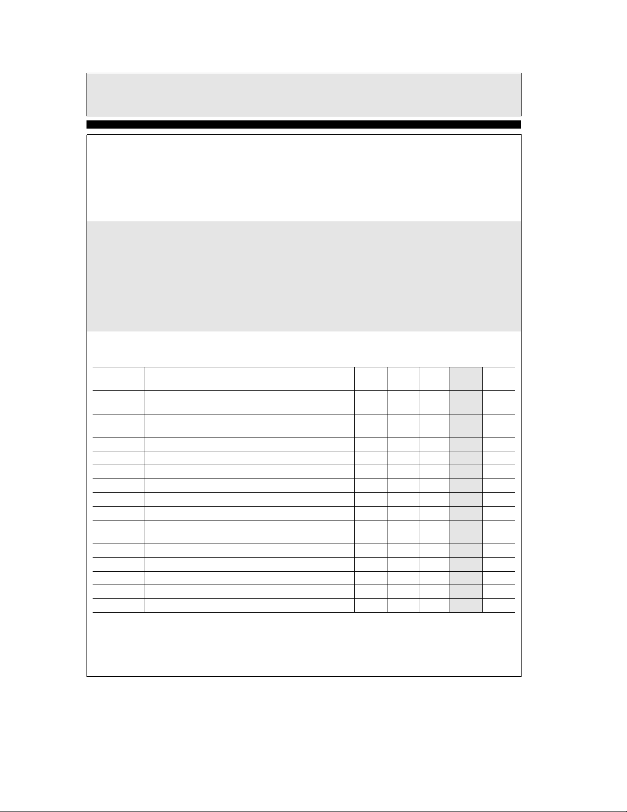
Test Circuit
Units
TD is 1.5in TD is 1.5in
Note: For typical performance curves, R
F
e
910X,R
G
e
100X,V
GAIN
3
e
1V, R
e
L
500X, and C
4452– 2
e
15 pF unless otherwise noted.
L
Page 4
EL4452C
Wideband Variable-Gain Amplifier with Gain of 10
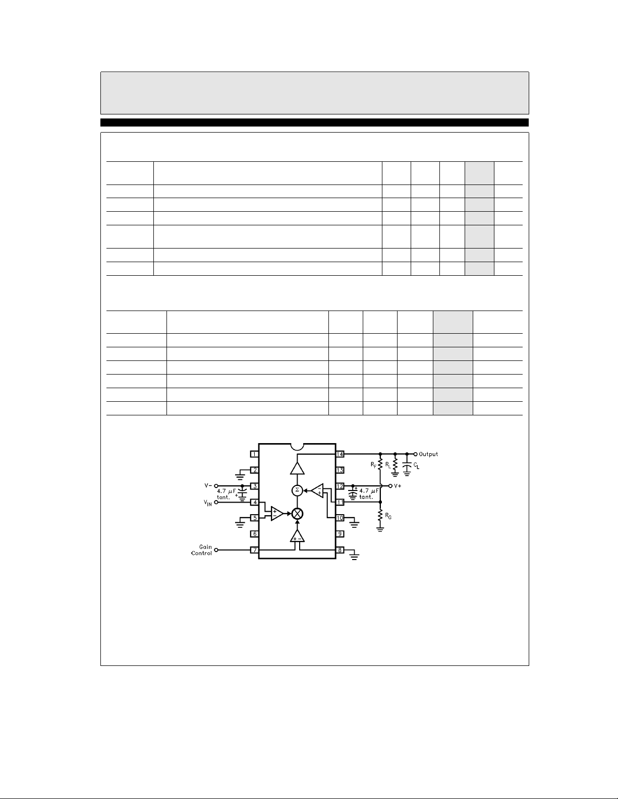
Typical Performance Curves
Frequency Response for
Various Feedback Divider Ratios
Frequency Response for
Various Gains
Frequency Response for
Various R
b
vs Supply Voltage
L,CL,VS
3 dB Bandwidth
4452– 3
e
g
5V
4452– 5
Frequency Response for
Various R
b
vs Die Temperature
L,CL,VS
3 dB Bandwidth
e
g
15V
4452– 4
4452– 6
4452– 7
4452– 8
4
Page 5

EL4452C
Wideband Variable-Gain Amplifier with Gain of 10
Typical Performance Curves
Gain andb3 dB Bandwidth
vs Load Resistance
Slew Rate
vs Supply Voltage
Ð Contd.
4452– 9
Input Common-Mode
Rejection Ratio
vs Frequency
Slew Rate
vs Die Temperature
4452– 10
Input Voltage Noise
vs Frequency
4452– 11
4452– 13
4452– 12
Nonlinearity
vs Input Signal
4452– 14
5
Page 6

EL4452C
Wideband Variable-Gain Amplifier with Gain of 10
Typical Performance Curves
Bias Current
vs Die Temperature
Change in
and V
V
G, 100%
vs Die Temperature
G, 0%
Ð Contd.
4452– 15
Gain vs V
V
vs Supply Voltage
G, 0%
and V
GAIN
G, 100%
4452– 16
Common Mode
Input Range
vs Supply Voltage
4452– 17
4452– 19
4452– 18
Supply Current
vs Supply Voltage
4452– 20
6
Page 7

EL4452C
Wideband Variable-Gain Amplifier with Gain of 10
Typical Performance Curves
Contd.
Supply Current
vs Die Temperature
14-Pin Package
Power Dissipation vs
Ambient Temperature
Ð
4452– 21
Applications Information
The EL4452 is a complete two-quadrant multiplier/gain control with 50 MHz bandwidth. It has
three sets of inputs; a differential signal input
V
, a differential gain-controlling input V
IN
and another differential input which is used to
complete a feedback loop with the output. Here is
a typical connection:
The gain of the feedback divider is H. The transfer function of the part is
c
e
V
A
OUT
O
b
(V
VFB)).
REF
VFBis connected to V
network, so V
(((V
IN
FB
a)b
(V
e
b
))c((V
IN
OUT
HcV
a)b
GAIN
through a feedback
OUT.AO
loop gain of the amplifier, and is approximately
3300. The large value of A
((V
x
IN
a)b
0.
(V
b
IN
))c(/2 ((V
GAIN
a)b
O
(V
drives
GAIN
b))a
GAIN
4451-23
b))a
(V
GAIN
is the open-
b
(V
VFB)
REF
,
4452– 22
Rearranging and substituting for V
e
a)b
V
OUT
(((V
IN
(V
b
IN
))c(/2 ((V
GAIN
or
c
e
V
(V
OUT
IN
7
(/2 V
GAIN
a
V
)/H
REF
a)b
FB
(V
))aV
GAIN
REF
)/H,
Page 8

EL4452C
Wideband Variable-Gain Amplifier with Gain of 10
Applications Information
Ð Contd.
Thus the output is equal to the difference of the
V
’s times the difference of V
IN
by V
, all gained up by the feedback divider
REF
GAIN’S
and offset
ratio. The EL4452 is stable for a divider ratio of
(/10, and the divider may be set for higher output
gain, although with the traditional loss of bandwidth.
It is important to keep the feedback divider’s impedance at the FB terminal low so that stray capacitance does not diminish the loop’s phase
margin. The pole caused by the parallel impedance of the feedback resistors and stray capacitance should be at least 130 MHz; typical strays
of 3 pF thus require a feedback impedance of
400X or less. Alternatively, a small capacitor
across R
can be used to create more of a fre-
F
quency-compensated divider. The value of the capacitor should scale with the parasitic capacitance at the FB input. It is also practical to place
small capacitors across both the feedback and the
gain resistors (whose values maintain the desired
gain) to swamp out parasitics. For instance, a
3 pF capacitor across R
and 27 pF to ground
F
will dominate parasitic effects in a (/10 divider
and allow a higher divider resistance.
The REF pin can be used as the output’s ground
reference, for DC offsetting of the output, or it
can be used to sum in another signal.
Gain-Control Characteristics
The quantity V
bounded as 0
s
V
in the above equations is
GAIN
s
GAIN
2, even though the externally applied voltages exceed this range. Actually, the gain transfer function around 0 and 2V is
‘‘soft’’; that is, the gain does not clip abruptly
below the 0%-V
100%-V
applied to V
level. An overdrive of 0.3V must be
GAIN
GAIN
Because the 0%- or 100%- V
voltage nor above the
GAIN
to obtain truly 0% or 100%.
levels cannot
GAIN
be precisely determined, they are extrapolated
from two points measured inside the slope of the
gain transfer curve. Generally, an applied V
GAIN
range ofb0.5V toa2.5V will assure the full numerical span of 0
s
V
GAIN
s
2.
The gain control has a small-signal bandwidth
equal to the V
channel bandwidth, and over-
IN
load recovery resolves in about 20 nsec.
Input Connections
The input transistors can be driven from resistive
and capacitive sources, but are capable of oscillation when presented with an inductive input. It
takes about 80nH of series inductance to make
the inputs actually oscillate, equivalent to four
inches of unshielded wiring or 6
of unterminat-
×
ed input transmission line. The oscillation has a
characteristic frequency of 500 MHz. Often placing one’s finger (via a metal probe) or an oscilloscope probe on the input will kill the oscillation.
Normal high-frequency construction obviates
any such problems, where the input source is reasonably close to the input. If this is not possible,
one can insert series resistors of around 51X to
de-Q the inputs.
Signal Amplitudes
Signal input common-mode voltage must be between (V
b)a
2.5V and (Va)b2.5V to ensure
linearity. Additionally, the differential voltage on
any input stage must be limited to
g
6V to pre-
vent damage. The differential signal range is
g
0.5V in the EL4452. The input range is sub-
stantially constant with temperature.
The Ground Pin
The ground pin draws only 6 mA maximum DC
current, and may be biased anywhere between
b)a
(V
2.5V and (Va)b3.5V. The ground pin is
connected to the IC’s substrate and frequency
compensation components. It serves as a shield
within the IC and enhances input stage CMRR
and feedthrough over frequency, and if connected
to a potential other than ground, it must be bypassed.
Power Supplies
The EL4452 operates with power supplies from
g
3V tog15V. The supplies may be of different
voltages as long as the requirements of the
ground pin are observed (see the Ground Pin section). The supplies should be bypassed close to
the device with short leads. 4.7 mF tantalum capacitors are very good, and no smaller bypasses
need be placed in parallel. Capacitors as small as
0.01 mF can be used if small load currents flow.
Single-polarity supplies, such as
a
5V can be used, where the ground pin is connected to
a
5V and Vbto ground. The inputs
a
12V with
8
Page 9

EL4452C
Wideband Variable-Gain Amplifier with Gain of 10
Applications Information
Ð Contd.
and outputs will have to have their levels shifted
above ground to accommodate the lack of negative supply.
The power dissipation of the EL4452 increases
with power supply voltage, and this must be
compatible with the package chosen. This is a
close estimate for the dissipation of a circuit:
2cV
c
IS, maxa(V
S
b
VO)cVO/R
S
PAR
e
P
D
where IS, max is the maximum supply current
V
S
is the
g
supply voltage (assumed
equal)
V
is the output voltage
O
R
is the parallel of all resistors loading
PAR
the output
For instance, the EL4452 draws a maximum of
18mA. With light loading, R
dissipation with
g
5V supplies is 180 mW. The
PAR
x
%
and the
maximum supply voltage that the device can run
on for a given P
, max
S
e
(P
V
and other parameters is
D
2
a
V
/R
D
O
PAR
)/(2I
S
a
VO/R
PAR
)
The maximum dissipation a package can offer is
Output Loading
The output stage of the EL4452 is very powerful.
It can typically source 80 mA and sink 120 mA.
Of course, this is too much current to sustain and
the part will eventually be destroyed by excessive
dissipation or by metal traces on the die opening.
The metal traces are completely reliable while delivering the 30 mA continuous output given in
the Absolute Maximum Ratings table in this
data sheet, or higher purely transient currents.
Gain changes only 0.2% from no load to a 100X
load. Heavy resistive loading will degrade frequency response and distortion for loads
k
100X.
Capacitive loads will cause peaking in the frequency response. If capacitive loads must be driven, a small-valued series resistor can be used to
isolate it. 12X to 51X should suffice. A 22X series
resistor will limit peaking to 1 dB with even a
220 pF load.
AGC Circuits
The basic AGC (automatic gain control) loop is
this:
P
, maxe(TJ, maxbTA, max) / i
D
JA
Where TJ, max is the maximum die tempera-
ture, 150
C for reliability, less to re-
§
tain optimum electrical performance
T
, max is the ambient temperature,
A
70
C for commercial and 85§C for in-
§
dustrial range
i
is the thermal resistance of the
JA
mounted package, obtained from
data sheet dissipation curves
The more difficult case is the SO-14 package.
With a maximum die temperature of 150
maximum ambient temperature of 85
C and a
§
C, the 65§C
§
temperature rise and package thermal resistance
of 120
C/W gives a dissipation of 542 mW at
§
85
C. This allows the full maximum operating
§
supply voltage unloaded, but reduced if loaded.
Basic AGC Loop
4452– 24
A multiplier scales the input signal and provides
necessary gain and buffers the signal presented
to the output load, a level detector (shown schematically here as a diode) converts some measure
of the output signal amplitude to a DC level, a
low-pass filter attenuates any signal ripple present on that DC level, and an amplifier compares
that level to a reference and amplifies the error to
create a gain-control voltage for the multiplier.
The circuitry is a servo that attempts to keep the
output amplitude constant by continuously adjusting the multiplier’s gain control input.
9
Page 10

EL4452C
Wideband Variable-Gain Amplifier with Gain of 10
Applications Information
Most AGC’s deal with repetitive input signals
that are capacitively coupled. It is generally desirable to keep DC offsets from mixing with AC
signals and fooling the level detector into maintaining the DC output offset level constant, rather than a smaller AC component. To that end,
either the level detector is AC-coupled, or the reference voltage must be made greater than the
maximum multiplier gain times the input offset.
For instance, if the level detector output equaled
Ð Contd.
the reference voltage at 1V of EL4452 output, the
8 mV of input offset would require a maximum
gain of 125 through the EL4452. Bias current-induced offsets could increase this further.
Depending on the nature of the signal, different
level detector strategies will be employed. If the
system goal is to prevent overload of subsequent
stages, peak detectors are preferred. Other strategies use an RMS detector to maintain constant
output power. Here is a simple AGC using peak
detection:
4452– 25
10
Page 11

EL4452C
Wideband Variable-Gain Amplifier with Gain of 10
Applications Information
The output of the EL4452 drives a diode detector
which is compared to V
tor. Its output feeds the gain-control input of the
EL4452. The integrator’s output is attenuated by
the2kXand 2.7 kX resistors to prevent the op-
amp from overloading the gain-control pin during zero input conditions. The 510 kX resistor
provides a pull-down current to the peak level
storage capacitor C1 to allow it to drift negative
when output amplitude reduces. Thus the detector is of fast attack and slow decay design, able to
reduce AGC gain rapidly when signal amplitude
suddenly increases, and increases gain slowly
when the input drops out momentarily. The value of C1 determines drop-out reaction rates, and
the value of C
as well as the amount of ripple on the gain-control line. C2 can be used to reduce this ripple fur-
affects overall loop time constant
F
by an offset integra-
REF
Ð Contd.
ther, although it contributes to loop overshoot
when input amplitude changes suddenly. The opamp can be any inexpensive low-frequency type.
The major problem with diode detectors is their
large and variable forward voltage. They require
at leasta2V
reliably, and the forward voltage should be compensated by including a negative V
V
. Even this is only moderately successful.
REF
At the expense of bandwidth, op-amp circuits can
greatly improve diode rectifiers (see ‘‘An Improved Peak Detector’’, an Elantec application
note). Fortunately, the detector will see a constant amplitude of signal if the AGC is operating
correctly.
A better-calibrated method is to use a four-quadrant multiplier as a square-law detector. Here is a
circuit employing the EL4450:
peak output signal to function
P-P
D
added to
4452– 26
11
Page 12

EL4452C
Wideband Variable-Gain Amplifier with Gain of 10
EL4452CDecember 1994 Rev A
Applications Information
Ð Contd.
In this circuit, the EL4450 not only calculates the
square of the input, but also provides the offset
integrator function. The product of the two multiplier inputs adds to the
b
Reference input and
are passed to the output amplifier, which
through C
behaves as a pseudo-integrator. The
F
‘‘integrator’’ gain does not pass through zero at
high frequencies but has a zero at 1/(2
qC
c
F
kX). This zero is cancelled by the pole caused by
the second capacitor of value C
EL4452
b
V
input. ThebReference can be
GAIN
connected at the
F
exchanged for a positive reference by connecting
it to the ground return of the 1 kX resistor at the
FB terminal and grounding REF.
As a general consideration, the input signal applied to an EL4452 should be kept below about
250 mV peak for good linearity. If the AGC were
designed to produce a 1V peak output, the input
range would be 100 mV–250 mV peak when the
EL4452 has a feedback network that establishes a
maximum gain of 10. This is an input range of
only 2.5:1 for precise output regulation. Raising
the maximum gain to 25 allows a 40 mV – 250 mV
1
input range with the output still regulated, better
than 6:1. Unfortunately, the bandwidth will be
reduced. Bandwidth can be maintained by adding
a high frequency op-amp cascaded with the output to make up gain beyond the 10 of the
EL4452, current feedback devices being the most
flexible. The op-amp’s input should be capacitor
coupled to prevent gained-up offsets from confusing the level detector during AGC control line
variations.
General Disclaimer
Specifications contained in this data sheet are in effect as of the publication date shown. Elantec, Inc. reserves the right to make changes
in the circuitry or specifications contained herein at any time without notice. Elantec, Inc. assumes no responsibility for the use of any
circuits described herein and makes no representations that they are free from patent infringement.
WARNING Ð Life Support Policy
Elantec, Inc. products are not authorized for and should not be
used within Life Support Systems without the specific written
consent of Elantec, Inc. Life Support systems are equipment in-
Elantec, Inc.
1996 Tarob Court
Milpitas, CA 95035
Telephone: (408) 945-1323
(800) 333-6314
Fax: (408) 945-9305
European Office: 44-71-482-4596
tended to support or sustain life and whose failure to perform
when properly used in accordance with instructions provided can
be reasonably expected to result in significant personal injury or
death. Users contemplating application of Elantec, Inc. products
in Life Support Systems are requested to contact Elantec, Inc.
factory headquarters to establish suitable terms & conditions for
these applications. Elantec, Inc.’s warranty is limited to replacement of defective components and does not cover injury to persons or property or other consequential damages.
Printed in U.S.A.12
 Loading...