

Page 1
EL4451C
Wideband Variable-Gain Amplifier, Gain of 2
EL4451C October 1994 Rev A
Features
# Complete variable-gain amplifier
with output amplifier, requires
no extra components
# Excellent linearity of 0.2%
# 70 MHz signal bandwidth
# Operates on
g
5V tog15V
supplies
# All inputs are differential
# 400V/ms slew rate
l
#
70dB attenuation@4 MHz
Applications
# Leveling of varying inputs
# Variable filters
# Fading
# Text insertion into video
Ordering Information
Part No. Temp. Range Package Outline
EL4451CNb40§Ctoa85§C 14-Pin P-DIP MDP0031
EL4451CSb40§Ctoa85§C 14-Lead SO MDP0027
General Description
The EL4451C is a complete variable gain circuit. It offers wide
bandwidth and excellent linearity while including a powerful
output voltage amplifier, drawing modest supply current.
The EL4451C operates on
analog input range of
g
5V tog15V supplies and has an
g
2V, making it ideal for video signal
processing. AC characteristics do not change appreciably over
g
the
5V tog15V supply range.
The circuit has an operational temperature range of
a
85§C and is packaged in plastic 14-pin DIP and 14-lead SO.
The EL4451C is fabricated with Elantec’s proprietary complementary bipolar process which provides excellent signal symmetry and is free from latch up.
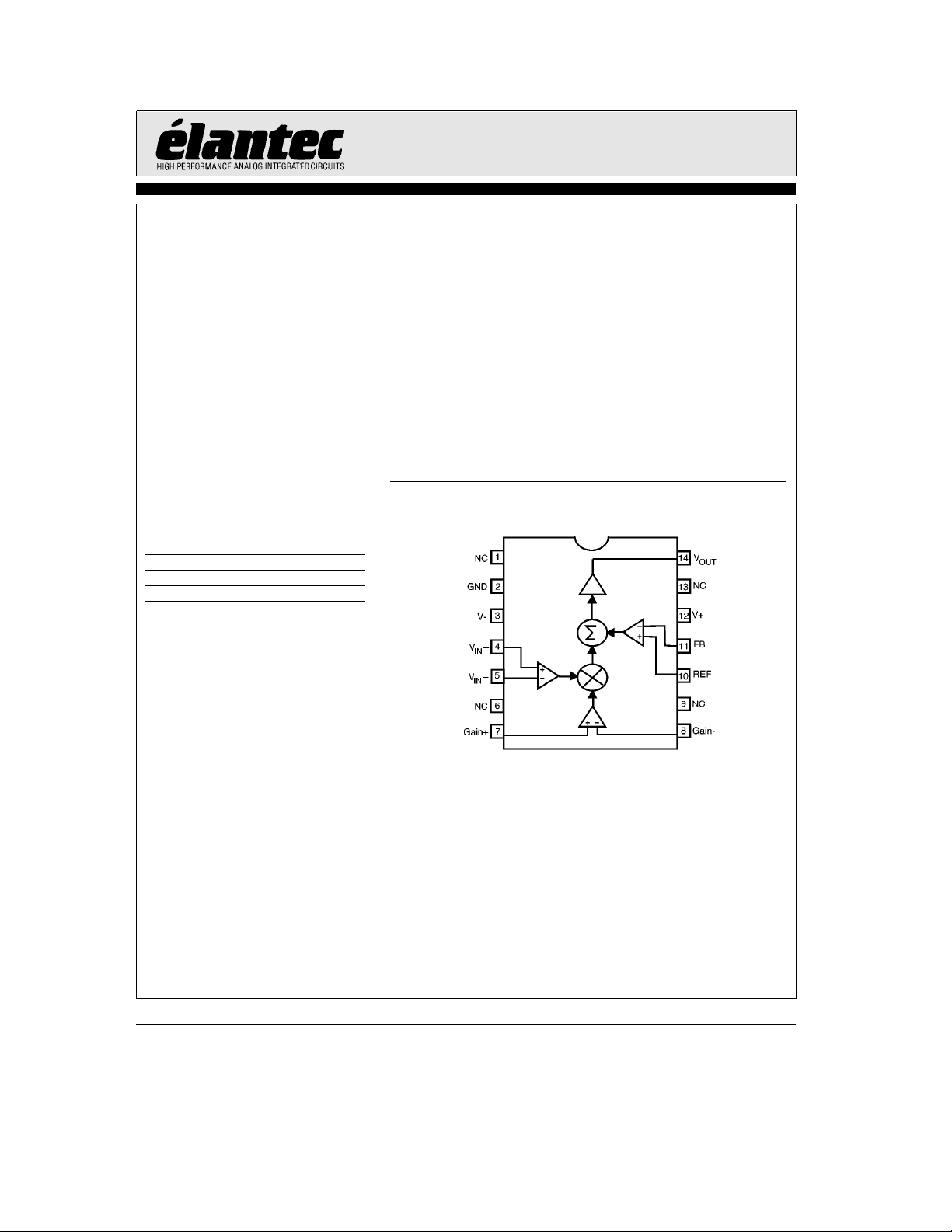
Connection Diagram
Ý
b
40§Cto
4451-1
Note: All information contained in this data sheet has been carefully checked and is believed to be accurate as of the date of publication; however, this data sheet cannot be a ‘‘controlled document’’. Current revisions, if any, to these
specifications are maintained at the factory and are available upon your request. We recommend checking the revision level before finalization of your design documentation.
©
1994 Elantec, Inc.
Page 2
EL4451C
Wideband Variable-Gain Amplifier, Gain of 2
Absolute Maximum Ratings
a
Positive Supply Voltage 16.5V
V
V
Vato VbSupply Voltage 33V
S
V
Voltage at any Input or Feedback Vato V
IN
DVINDifference between Pairs
of Inputs or Feedback 6V
I
Current into any Input, or Feedback Pin 4mA
IN
Important Note:
All parameters having Min/Max specifications are guaranteed. The Test Level column indicates the specific device testing actually
performed during production and Quality inspection. Elantec performs most electrical tests using modern high-speed automatic test
equipment, specifically the LTX77 Series system. Unless otherwise noted, all tests are pulsed tests, therefore T
Test Level Test Procedure
I 100% production tested and QA sample tested per QA test plan QCX0002.
II 100% production tested at T
III QA sample tested per QA test plan QCX0002.
IV Parameter is guaranteed (but not tested) by Design and Characterization Data.
V Parameter is typical value at T
T
MAX
and T
MIN
A
per QA test plan QCX0002.
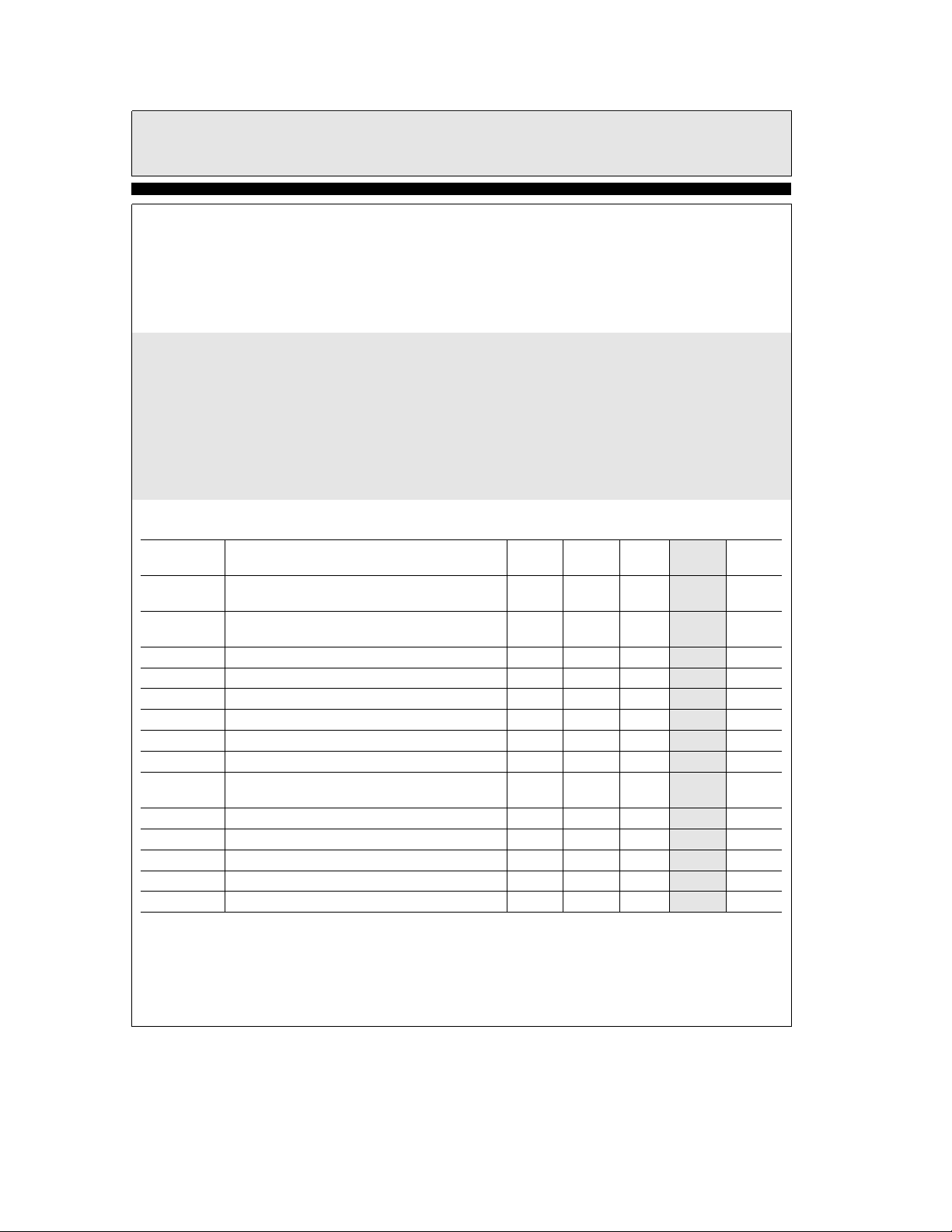
Open-Loop DC Electrical Characteristics
Parameter Description Min Typ Max
V
V
V
DIFF
CM
OS
Signal input differential input voltage - Clipping 1.8 2.0 I V
0.2% nonlinearity 1.3 V V
Common-mode range of VIN;V
e
g
V
15V
s
Input offset voltage 7 25 I mV
e
(T
25§C)
A
e
25§C and QA sample tested at T
e
25§C for information purposes only.
A
e
DIFF
b
0, V
I
OUT
P
D
T
A
T
S
e
g
5V
s
Continuous Output Current 30mA
Maximum Power Dissipation See Curves
e
J
25§C, R
Level
b
40§Ctoa85§C
b
60§Ctoa150§C
e
T
TA.
C
e
500X.
L
Test
Units
Operating Temperature Range
Storage Temperature Range
e
25§C,
A
Power Supplies atg5V, T
g
2.0
g
2.8 I V
g
12.8 V V
e
A
VOS, FB Output offset voltage 8 25 I mV
V
G, 100%
V
G, 0%
V
G, 1V
I
B
I
OS
NL Nonlinearity, VINbetweenb1V anda1V, V
Ft Signal feedthrough, V
RIN,V
IN
Extrapolated voltage for 100% gain 1.9 2.1 2.2 I V
Extrapolated voltage for 0% gain
Gain at V
e
1V 0.95 1.05 1.15 I V/V
GAIN
Input bias current (all inputs)
Input offset current between V
a
Gain
and Gainb, FB and Ref
Input resistance, V
IN
G
eb
IN
1V
a
and V
b
b
b
,
IN
e
1V 0.2 0.5 I %
G
100 230 I KX
0.16
20
b
0.06 0.06 I V
b
90 I mA
0.2 4 I mA
b
100
b
70 I dB
RIN, FB Input resistance, FB 200 460 V KX
R
IN,RGAIN
Input resistance, gain input 50 100 I KX
TD is 3.3in
2
Page 3
EL4451C
Wideband Variable-Gain Amplifier, Gain of 2
Open-Loop DC Electrical Characteristics
Power Supplies atg5V, T
e
25§C, R
A
Parameter Description Min Typ Max
CMRR Common-mode rejection ratio of V
PSRR Power supply rejection ratio of VOS,FB,V
V
O
I
SC
I
S
Output voltage swing V
e
(V
0, V
IN
Output short-circuit current 40 85 I mA
Supply current, V
e
500X.
L
IN
e
g
S
e
g
5V
S
e
varied) V
REF
e
g
15V 15.5 18 I mA
S
g
15V
S
Ð Contd.
Test
Level
70 90 I dB
5V tog15V 50 60 I dB
g
g
2.5
12.5
g
2.8
g
12.8
IV
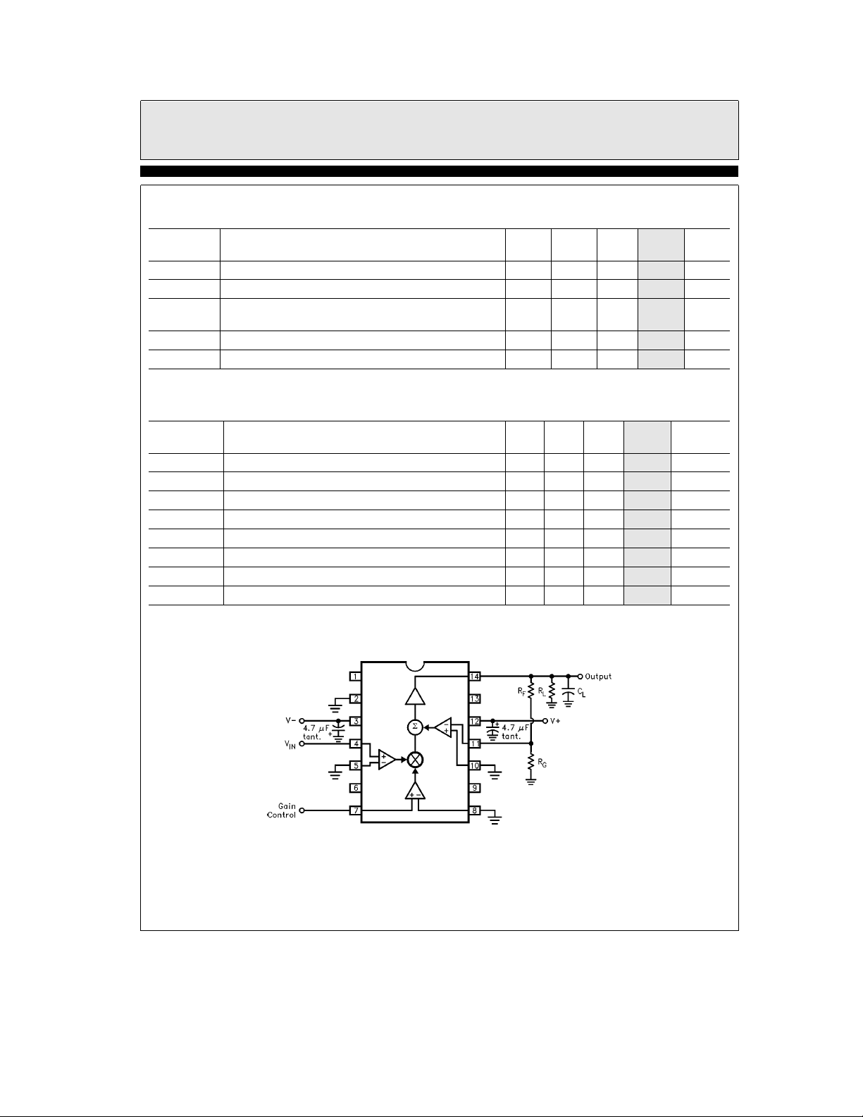
Closed-Loop AC Electrical Characteristics
Power supplies atg12V, T
e
25§C. R
A
Parameter Description Min Typ Max
BW,b3dB
b
3dB small-signal bandwidth, signal input 70 V MHz
BW,g0.1dB 0.1dB flatness bandwidth, signal input 10 V MHz
Peaking Frequency response peaking 0.6 V dB
BW, gain
SR Slew rate, V
V
N
b
3dB small-signal bandwidth, gain input 70 V MHz
OUT
Input referred noise voltage density 110 V nV/SHz
dG Differential gain error, Voffset betweenb0.7V anda0.7V 0.9 V %
di Differential phase error, Voffset betweenb0.7V anda0.7V 0. 2 V
L
e
500X,C
L
e
15pF, V
betweenb2V anda2V, R
e
1V
G
Test
Level
e
e
R
F
500X 400 V V/ms
G
Units
Units
§
TD is 1.8in TD is 1.8in
Test Circuit
Note: For typical performance curves, R
e
e %
0, R
F
G
,V
GAIN
e
1V, R
e
L
500X, and C
e
15 pF unless otherwise noted.
L
4451– 3
3
Page 4
EL4451C
Wideband Variable-Gain Amplifier, Gain of 2
Typical Performance Curves
Frequency Response
for Various Feedback
Divider Ratios
Gain,b3 dB Bandwidth,
and Peaking
vs Load Resistance
4451– 4
Frequency Response
for Various R
e
V
S
b
3 dB Bandwidth and Peaking
vs Supply Voltage
L,CL
g
5V
4451– 5
Frequency Response
for Various R
e
V
S
b
3 dB Bandwidth and Peaking
vs Die Temperature
L,CL
g
15V
4451– 6
Frequency Response for
Various Gain Settings
4451– 7
4451– 10
Slew Rate
vs Supply Voltage
4
4451– 8
4451– 11
Slew Rate
vs Die Temperature
4451– 9
4451– 12
Page 5

EL4451C
Wideband Variable-Gain Amplifier, Gain of 2
Typical Performance Curves
Common-Mode
Rejection Ratio
vs Frequency
4451– 13
Differential Gain Error
vs Input Offset Voltage
e
g
5V org12V
V
S
Ð Contd.
Input Voltage Noise
vs Frequency
Differential Phase Error
vs Input Offset Voltage
e
g
5V
V
S
4451– 14
Nonlinearity vs
Input Signal
Differential Phase Error
vs Input Offset Voltage
e
g
12V
V
S
4451– 15
Differential Gain
and Phase Errors
vs Gain Setting
4451– 16
4451– 19
4451– 17
Differential Gain
and Phase Errors
vs Load Resistance
4451– 20
4451– 18
5
Page 6

EL4451C
Wideband Variable-Gain Amplifier, Gain of 2
Typical Performance Curves
Gain vs V
Offset Voltage
vs Die Temperature
GAIN
4451– 21
Ð Contd.
Change in
and V
V
G, 100%
vs Die Temperature
Bias Current
vs Die Temperature
G, 0%
4451– 22
V
and V
G, 0%
vs Supply Voltage
Common Mode
Input Range
vs Supply Voltage
G, 100%
4451– 23
Supply Current
vs Die Temperature
4451– 24
4451– 27
Supply Current
vs Supply Voltage
6
4451– 25
4451– 28
14-Pin Package
Power Dissipation vs
Ambient Temperature
4451– 26
4451– 29
Page 7

EL4451C
Wideband Variable-Gain Amplifier, Gain of 2
Applications Information
The EL4451 is a complete two-quadrant multiplier/gain control with 70 MHz bandwidth. It has
three sets of inputs; a differential signal input
V
, a differential gain-controlling input V
IN
and another differential input which is used to
complete a feedback loop with the output. Here is
a typical connection:
The gain of the feedback divider is
R
G
e
H
.
a
R
R
G
F
The transfer function of the part is
c
e
V
A
OUT
b
(V
VFB)).
REF
VFBis connected to V
network, so V
a
(((V
O
IN
FB
)b(V
e
b
))c((V
IN
OUT
HcV
a)b
GAIN
through a feedback
OUT.AO
loop gain of the amplifier, and is approximately
600. The large value of A
a)b
((V
x
IN
0.
b
(V
))c((V
IN
GAIN
Rearranging and substituting for V
e
a)b
V
(((V
OUT
IN
b
(V
))c((V
IN
a)b
O
(V
GAIN
drives
b))a
GAIN
a)b
(V
FB
GAIN
or
c
e
V
(V
OUT
IN
V
GAIN
a
V
)/H
REF
Thus the output is equal to the difference of the
V
’s times the difference of V
IN
by V
, all gained up by the feedback divider
REF
GAIN’S
ratio. The EL4451 is stable for a direct connection between V
and FB, and the divider may
OUT
be used for higher output gain, although with the
traditional loss of bandwidth.
It is important to keep the feedback divider’s impedance at the FB terminal low so that stray capacitance does not diminish the loop’s phase
margin. The pole caused by the parallel impedance of the feedback resistors and stray capacitance should be at least 150 MHz; typical strays
of 3 pF thus require a feedback impedance of
GAIN
4451-2
b))a
(V
GAIN
is the open-
b
(V
VFB)
REF
))aV
REF
and offset
)/H,
360X or less. Alternatively, a small capacitor
across R
can be used to create more of a fre-
F
quency-compensated divider. The value of the capacitor should scale with the parasitic capacitance at the FB input. It is also practical to place
,
small capacitors across both the feedback and the
gain resistors (whose values maintain the desired
gain) to swamp out parasitics. For instance, two
10pF capacitors across equal divider resistors for
a maximum gain of 4 will dominate parasitic effects and allow a higher divider resistance.
The REF pin can be used as the output’s ground
reference, for DC offsetting of the output, or it
can be used to sum in another signal.
Gain-Control Characteristics
The quantity V
bounded as 0
s
V
in the above equations is
GAIN
s
2, even though the exter-
GAIN
nally applied voltages exceed this range. Actually, the gain transfer function around 0 and 2V is
‘‘soft’’; that is, the gain does not clip abruptly
below the 0%-V
100%-V
applied to V
level. An overdrive of 0.3V must be
GAIN
GAIN
Because the 0%- or 100%- V
voltage nor above the
GAIN
to obtain truly 0% or 100%.
levels cannot
GAIN
be precisely determined, they are extrapolated
from two points measured inside the slope of the
gain transfer curve. Generally, an applied V
range ofb0.5V toa2.5V will assure the full numerical span of 0
s
V
GAIN
s
2.
The gain control has a small-signal bandwidth
equal to the V
channel bandwidth, and over-
IN
load recovery resolves in about 20 nsec.
Input Connections
The input transistors can be driven from resistive
and capacitive sources, but are capable of oscillation when presented with an inductive input. It
takes about 80nH of series inductance to make
the inputs actually oscillate, equivalent to four
inches of unshielded wiring or 6
of unterminat-
×
ed input transmission line. The oscillation has a
characteristic frequency of 500 MHz. Often placing one’s finger (via a metal probe) or an oscilloscope probe on the input will kill the oscillation.
Normal high-frequency construction obviates
any such problems, where the input source is reasonably close to the input. If this is not possible,
one can insert series resistors of around 51X to
de-Q the inputs.
7
GAIN
Page 8

EL4451C
Wideband Variable-Gain Amplifier, Gain of 2
Applications Information
Ð Contd.
Signal Amplitudes
Signal input common-mode voltage must be between (V
b)a
3V and (Va)b3V to ensure linearity. Additionally, the differential voltage on any
input stage must be limited to
damage. The differential signal range is
g
6V to prevent
g
2V in
the EL4451. The input range is substantially constant with temperature.
The Ground Pin
The ground pin draws only 6m A maximum DC
current, and may be biased anywhere between
b)a
(V
2.5V and (Va)b3.5V. The ground pin is
connected to the IC’s substrate and frequency
compensation components. It serves as a shield
within the IC and enhances input stage CMRR
and feedthrough over frequency, and if connected
to a potential other than ground, it must be bypassed.
Power Supplies
The EL4451 works with any supplies fromg3V
g
to
15V. The supplies may be of different voltages as long as the requirements of the ground
pin are observed (see the Ground Pin section).
The supplies should be bypassed close to the device with short leads. 4.7mF tantalum capacitors
are very good, and no smaller bypasses need be
placed in parallel. Capacitors as small as 0.01mF
can be used if small load currents flow.
Single-polarity supplies, such as
a
5V can be used, where the ground pin is con-
nected to
a
5V and Vbto ground. The inputs
a
12V with
and outputs will have to have their levels shifted
above ground to accommodate the lack of negative supply.
The power dissipation of the EL4451 increases
with power supply voltage, and this must be
compatible with the package chosen. This is a
close estimate for the dissipation of a circuit:
c
e
P
2cV
D
IS, maxa(V
S
b
VO)cVO/R
S
PAR
where IS, max is the maximum supply current
V
is the
S
g
supply voltage (assumed
equal)
V
is the output voltage
O
R
is the parallel of all resistors loading
PAR
the output
For instance, the EL4451 draws a maximum of
%
18mA. With light loading, R
dissipation with
g
5V supplies is 180 mW. The
PAR
x
and the
maximum supply voltage that the device can run
on for a given P
VS, maxe(P
a
D
and other parameters is
D
2
V
/R
O
PAR
) / (2I
a
VO/R
S
PAR
)
The maximum dissipation a package can offer is
PD, maxe(TJ, maxbTA, max) / i
JA
Where TJ, max is the maximum die tempera-
ture, 150
C for reliability, less to re-
§
tain optimum electrical performance
T
, max is the ambient temperature,
A
70
C for commercial and 85§C for in-
§
dustrial range
i
is the thermal resistance of the
JA
mounted package, obtained from
data sheet dissipation curves
The more difficult case is the SO-14 package.
With a maximum die temperature of 150
maximum ambient temperature of 85
C and a
§
C, the 65§C
§
temperature rise and package thermal resistance
of 120
C/W gives a dissipation of 542 mW at
§
85
C. This allows the full maximum operating
§
supply voltage unloaded, but reduced if loaded.
Output Loading
The output stage of the EL4451 is very powerful.
It typically can source 80mA and sink 120mA. Of
course, this is too much current to sustain and
the part will eventually be destroyed by excessive
dissipation or by metal traces on the die opening.
The metal traces are completely reliable while delivering the 30mA continuous output given in the
Absolute Maximum Ratings table in this data
sheet, or higher purely transient currents.
Gain changes only 0.2% from no load to 100X
load. Heavy resistive loading will degrade frequency response and video distortion for loads
k
100X.
Capacitive loads will cause peaking in the frequency response. If capacitive loads must be driven, a small-valued series resistor can be used to
isolate it. 12X to 51X should suffice. A 22X series
resistor will limit peaking to 2.5 dB with even a
220pF load.
8
Page 9

EL4451C
Wideband Variable-Gain Amplifier, Gain of 2
Applications Information
Ð Contd.
Leveling Circuits
Often a variable-gain control is used to normalize
an input signal to a standard amplitude from a
modest range of possible input amplitude. A good
example is in video systems, where an unterminated cable will yield a twice-sized standard video amplitude, and an erroneously twice-terminated cable gives a 2/3-sized input.
Here is a
g
6 dB range preamplifier:
Linearized Leveling Amplifier
4451– 30
EL4451 Leveler Circuit
Attenuation Ratio
EL4451 Leveler Circuit
Attenuation Ratio
e
e
1.5
4451– 31
2
In this arrangement, the EL4451 outputs a mixture of the signal routed through the multiplier
and the REF terminal. The multiplier port produces the most distortion and needs to handle a
fraction of an oversized video input, whereas the
REF port is just like an op-amp input summing
into the output. Thus, for oversized inputs the
gain will be decreased and the majority of the
signal is routed through the linear REF terminal.
For undersized inputs, the gain is increased and
the multiplier’s contribution added to the output.
Here are some component values for two designs:
Attenuation
Ratio Bandwidth
1.5 200X 400X 300X 100X 200X 47 MHz
2 400X 400X 500X 100X 200X 28 MHz
R
FRGR1R2R3
b
3dB
With the higher attenuation ratio, the multiplier
sees a smaller input amplitude and distorts less,
however the higher output gain reduces circuit
bandwidth. As seen in the next curves, the peak
differential gain error is 0.47% for the attenuation ratio of 1.5, but only 0.27% with the gain of
2 constants. To maintain bandwidth, an external
op amp can be used instead of the R
F-RG
er to boost the EL4451’s output by the attenuation ratio.
Sinewave Oscillators
Generating a stable, low distortion sinewave has
long been a difficult task. Because a linear oscillator’s output tends to grow or diminish continuously, either a clipping circuit or automatic gain
control (AGC) is needed. Clipping circuits generate severe distortion which needs subsequent filtering, and AGC’s can be complicated.
9
4451– 32
divid-
Page 10

EL4451C
Wideband Variable-Gain Amplifier, Gain of 2
Applications Information
Ð Contd.
Here is the EL4451 used as an oscillator with simple AGC:
Low-Distortion Sinewave Oscillator
The oscillation frequency is set by the resonance
of a series-tuned circuit, which may be an L-C
combination or a crystal. At resonance, the series
impedance of the tuned circuit drops and its
phase lag is 0
over unity to sustain oscillation. The V
terminal is initially atb0.7V and the V
, so the EL4451 needs a gain just
§
GAIN
GAIN
Filters
The EL4451 can be connected to act as a voltagevariable integrator as shown:
EL4451 Connected As Variable Integrator
b
a
terminal at abouta2.1V, setting the maximum
gain in the EL4451. At such high gain, the loop
oscillates and output amplitude grows until D
rectifies more positive voltage at V
GAIN
b
1
, ultimately reducing gain until a stable 0.5Vrms output is produced.
4451– 33
Using a 2 MHz crystal, output distortion was
b
53 dBc, or 0.22%. Sideband modulation was
only 14 Hz wide at
b
90 dBc, limited by the filter
of the spectrum analyzer used.
The circuit works up to 30 MHz. A parallel-tuned
circuit can replace the 510X resistor and the 510X
resistor moved in place of the series-tuned element to allow grounding of the tuned components.
The input RC cancels a zero produced by the output op-amp feedback connection at
With the input RC connected V
1/sRC; without it V
OUT/VIN
e(1a
e
0
OUT/VIN
sRC)/sRC.
This variable integrator may be used in networks
such as the Bi-quad. In some applications the input RC may be omitted. If a negative gain is required, the V
IN
a
and V
b
terminals can be
IN
exchanged.
10
4451– 34
1/RC.
e
Page 11

EL4451C
Wideband Variable-Gain Amplifier, Gain of 2
Applications Information
A voltage-controlled equalizer and cable driver
can be constructed so:
Equalization and Line Driver Amplifier
Ð Contd.
4451– 35
The main signal path is via the REF pin. This
ensures maximum signal linearity, while the multiplier input is used to allow a variable amount of
frequency-shaped input from R
optimum linearity, the multiplier input is attenuated by R
depending on input signal amplitude, and R
might be set to 0. R1and R2should be set to provide sufficient peaking, depending on cable highfrequency losses, at maximum gain. R
are chosen to provide the desired circuit gain, including backmatch resistor loss.
and R2. This may not be necessary,
1
, and C. For
1,R2
and R
F
1
G
11
Page 12

EL4451C
Wideband Variable-Gain Amplifier, Gain of 2
EL4451COctober 1994 Rev A
General Disclaimer
Specifications contained in this data sheet are in effect as of the publication date shown. Elantec, Inc. reserves the right to make changes
in the circuitry or specifications contained herein at any time without notice. Elantec, Inc. assumes no responsibility for the use of any
circuits described herein and makes no representations that they are free from patent infringement.
WARNING Ð Life Support Policy
Elantec, Inc. products are not authorized for and should not be
used within Life Support Systems without the specific written
consent of Elantec, Inc. Life Support systems are equipment in-
Elantec, Inc.
1996 Tarob Court
Milpitas, CA 95035
Telephone: (408) 945-1323
(800) 333-6314
Fax: (408) 945-9305
European Office: 44-71-482-4596
tended to support or sustain life and whose failure to perform
when properly used in accordance with instructions provided can
be reasonably expected to result in significant personal injury or
death. Users contemplating application of Elantec, Inc. products
in Life Support Systems are requested to contact Elantec, Inc.
factory headquarters to establish suitable terms & conditions for
these applications. Elantec, Inc.’s warranty is limited to replacement of defective components and does not cover injury to persons or property or other consequential damages.
Printed in U.S.A.12
 Loading...