

Page 1
EL4450C
Wideband Four-Quadrant Multiplier
EL4450C
Features
• Complete four-quadrant multiplier
with output amp—requires no
extra components
• Good linearity of 0.3%
• 90 MHz bandwidth for both X and
Y inputs
• Operates on ±5V to ±15V supplies
• All inputs are differential
• 400V/µs slew rate
Applications
• Modulation/Demodulation
• RMS computation
• Real-time power computation
• Nonlinearity correction/generation
Ordering Information
Part No. Temp. Range Package Outline #
EL4450CN -40°C to +85°C 14-Pin P-DIP MDP0031 EL4450CS -40°C to +85°C 14-Lead SO MDP0027
General Description
The EL4450C is a complete four-quadrant multiplier circuit. It offers
wide bandwidth and go od line arity while incl uding a powerfu l outp ut
voltage amplifier, drawing modest supply current.
The EL4450C operates on ±5V supplies and has an analog input range
of ±2V, making it ideal for video signal processing. AC characteristics
do not vary over the ±5V t o ±15V supply range.
The multiplier has an operational temperature range of -40°C to
+85°C and are packaged in plast ic 14-pin P-DIP and SO.
© 1995 Elantec, Inc.
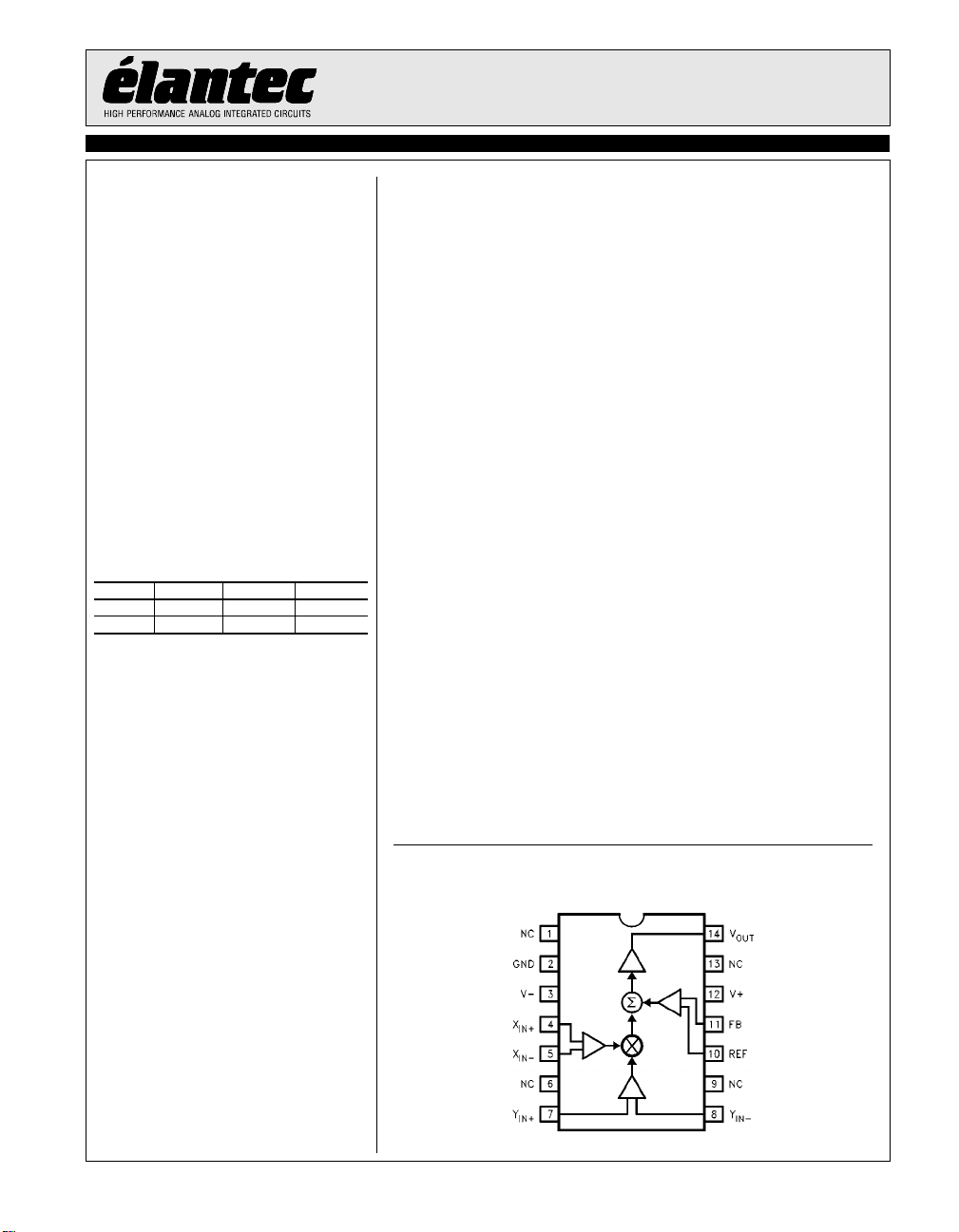
Connection Diagrams
January 1996 Rev B
Page 2
EL4450C
Wideband Four-Quadrant Multiplier
EL4450C
Absolute Maximum Ratings (T
V+ Positive Supply Voltage 16.5V
V+ to V- Supply Voltage 33V
V
S
V
Voltage at any Input or Feedback V+ to V-
IN
Difference between Pairs of Inputs or Feedback 6V
V
IN
Current into any Input or Feedback Pin 4 mA
I
IN
= 25 °C)
A
Output Current 30 mA
I
OUT
Maximum Power Dissipation See Curves
P
D
T
Operating Temperature Range -40°C to +85°C
A
Storage Temperature Range -60°C to +150°C
T
S
Important Note:
All parameters having Min/Max specifications are guaranteed. The Test Level column indicates the specific device testing actually performed during
production and Quality inspection. Elantec performs most electrical tests using modern high-speed automatic test equipment, specifically the LTX77
Series system. Unless otherwise noted, all tests are pulsed tests, therefor T
= TC = TA.
J
Test Level Test Procedure
I 100% production tested and QA sample tested per QA test plan QCX0002.
II 100% production tested at T
= 25°C and QA sample tested at TA = 25°C, T
A
MAX
and T
per QA test plan QCX0002.
MIN
III QA sample tested per QA test plan QCX0002.
IV Parameter is guaranteed (but not tested) by Design and Characterization Data.
V Parameter is typical value at T
= 25°C for information purposes only.
A
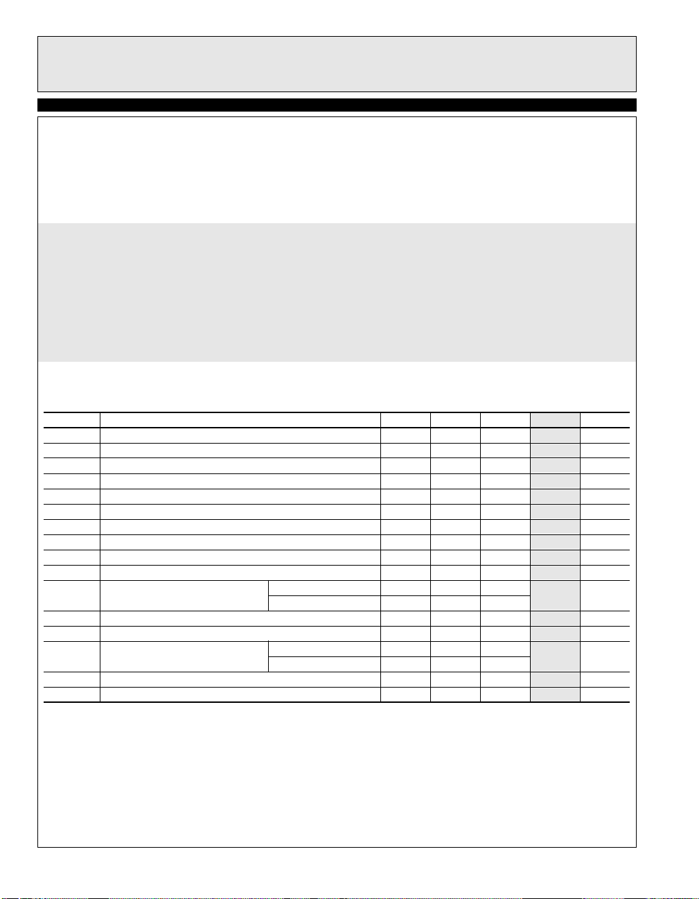
Open-Loop DC Electrical Characteristics
Power Supplies at ±5V, TA = 25°C, VFB = V
Parameter Description Min Typ Max
V
DIFF
Differential Input Voltage—Clipping 1.8 2.0 IV
0.2% nonlinearity 1.0
V
CM
V
OS
I
B
I
OS
Gain Gain Factor of V
Common-Mode Range of V
= ±15V ±12.5 ±12.8 IV
V
S
Input Offset Voltage 8 35 ImV
Input Bias Current 9 20 IµA
Input Offset Current between XIN+ and XIN-, YIN+ and YIN-, REF and FB 0.5 4 IµA
= Gain × XIN+ × Y
OUT
NLx Nonlinearity of X Input; XIN between -1V and +1V 0.3 0.7 I%
NLy Nonlinearity of Y Input; Y
R
IN
Input resistance X
CMRR Common-Mode Rejection Ratio, X
PSRR Power -Supply Rejection Ratio, FB 60 72
V
O
I
SC
I
S
Output Voltage Swing
= 0, V
(V
IN
REF
Varied)
Output Short-Circuit Current 40 85 ImA Supply Current, VS = ±15V 15.4 18 ImA
.
OUT
Test Level Units
VV
= 0, VS = ±5V ±2.5 ±2.8 IV
DIFF
IN
between -1V and +1V 0.2 0.35 I%
IN
to X
, Y
IN+
to Y
IN-
IN+
0.45 0.5 0.55 I V/V
, 230 VkΩ
IN-
2
REF to FB 90
IN
and Y
IN
70 90 IdB
IdB
V
= ±5V ± 2.5 ±2.8 IV
S
= ±15V ±12.5 ±12.8
V
S
2
Page 3

Wideband Four-Quadrant Multiplier
Closed-Loop AC Electrical Characteristics
Power Supplies at ±12V, TA = 25°C, RL = 500¾, CL = 15pF
Parameter Description Min Typ Max
BW, -3 dB -3 dB Small-Signal Bandwidth, X or Y 90
BW, ±0.1 dB 0.1 dB Flatness Bandwidth 10
Peaking Frequency Response Peaking 1.0
SR Slew Rate, V
V
N
Input-Referred Noise Voltage Density 100 V nV/Hz
between -2V and +2V 300 400 I V/µs
OUT
Test Circuit
EL4450C
EL4450C
Test Level Units
V MHz
V MHz
VdB
Note: For typical performance curves, RF = 0, RG = ×, VS = ±5V, RL = 500¾, and CL = 15 pF unless otherwise noted.
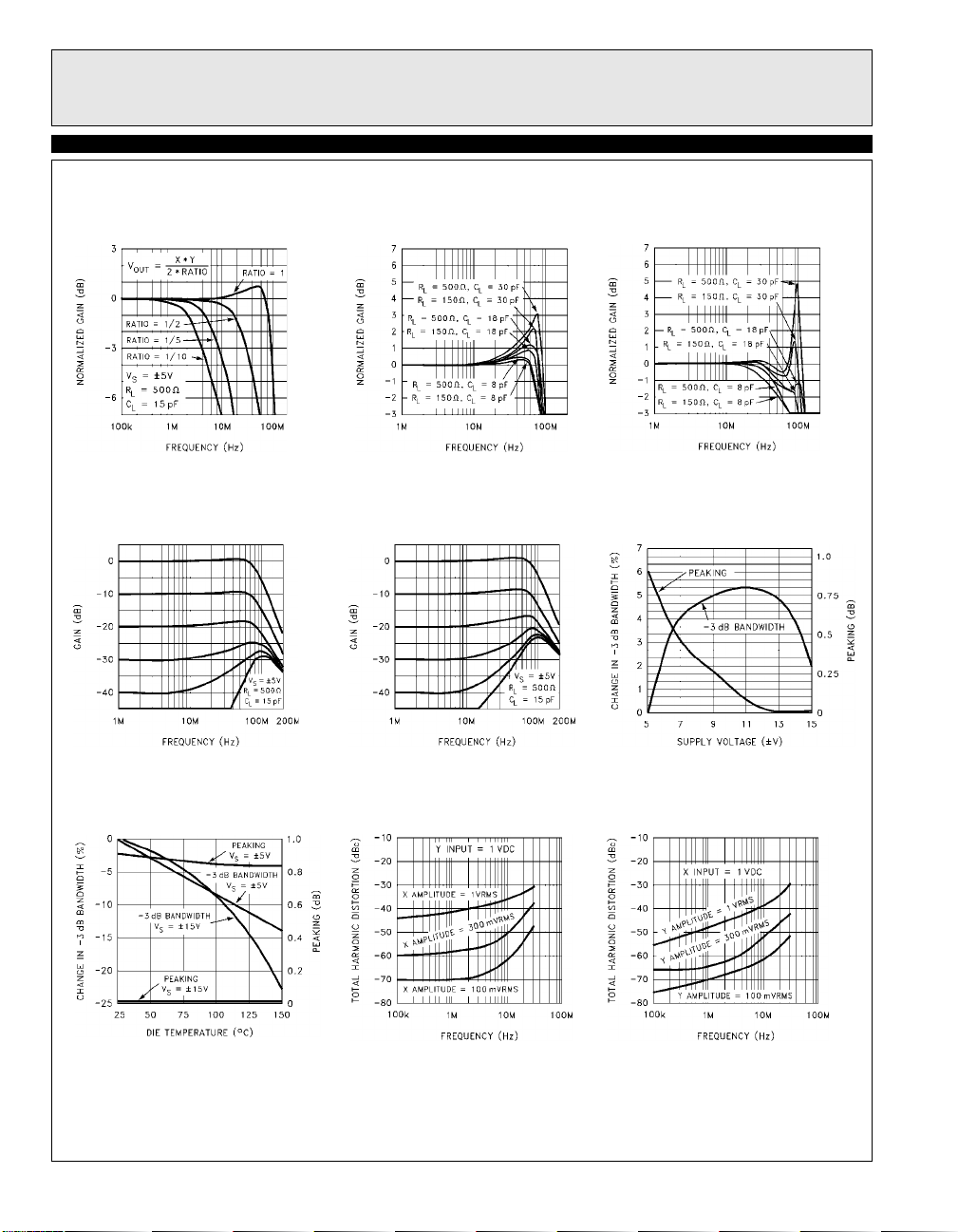
Typical Performance Curves
Transfer Function of X Input for
Various Y Inputs
Transfer Function of Y Input for
Various X Inputs
3
Page 4
EL4450C
Wideband Four-Quadrant Multiplier
EL4450C
Frequency Response
for Various Feedback
Divider Ratios
X Input Frequency Response
for Various Y DC Inputs
Frequency Response
for Various RL, C
VS = ±5V
Y Input Frequency Response
for Various X DC Inputs
L
Frequency Response
for Various RL, C
VS = ±15V
-3 dB Bandwidth
and Peaking
vs Supply Voltage
L
Change in Bandwidth
and Peaking vs Temperature
Total Harmonic Distortion
of X Input vs Frequency
4
Total Harmonic Distortion
of Y Input vs Frequency
Page 5
EL4450C
Wideband Four-Quadrant Multiplier
EL4450C
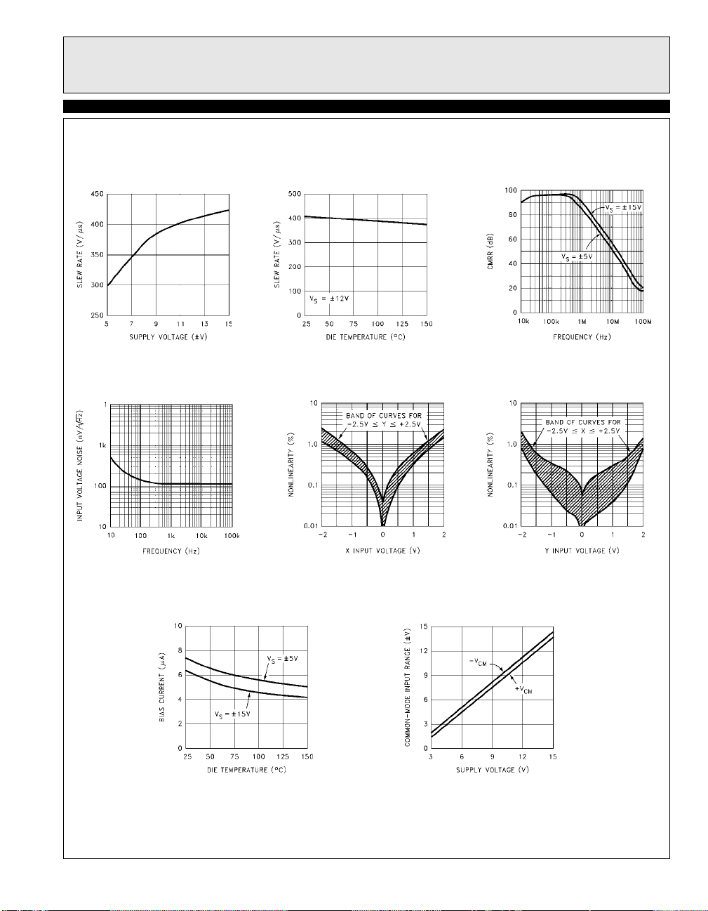
Slew Rate
vs Supply Voltage
Input Voltage Noise
vs Frequency
Slew Rate
vs Die Temperature
Nonlinearity of X Input
CMRR vs Frequency
Nonlinearity of Y Input
Bias Current
vs Die Temperature
Common-Mode Input Range
vs Supply Voltage
5
Page 6
EL4450C
Wideband Four-Quadrant Multiplier
EL4450C
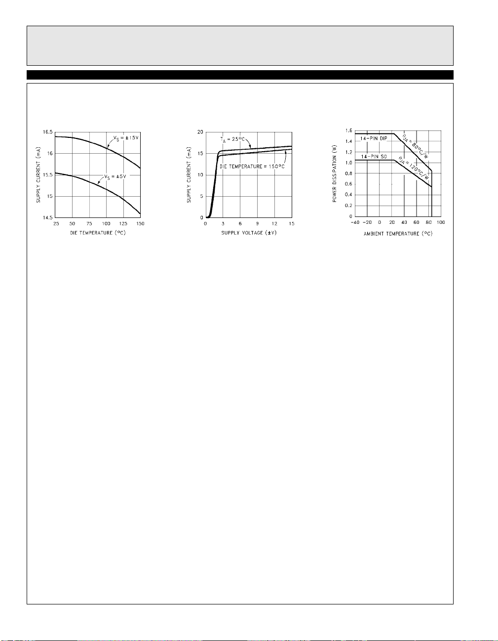
Supply Current
vs Die Temperature
Supply Current
vs Supply Voltage
14-Pin Package
Power Dissipation vs
Ambient Temperature
6
Page 7
Applications Information
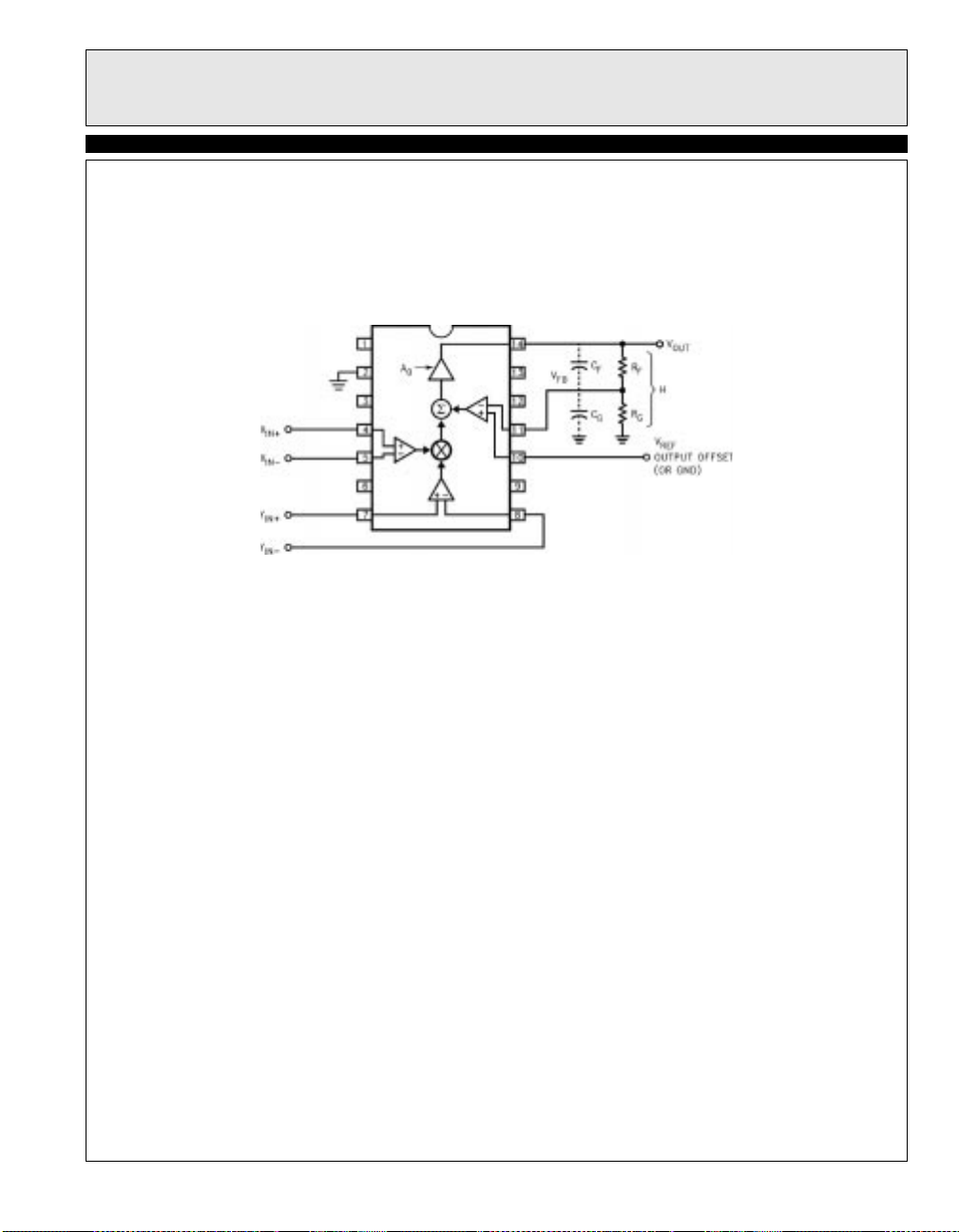
The EL4450 is a complete four-quadrant multiplier with
90 MHz bandwidth. It has three sets of inputs; a differential multiplying X-input, a differential multiplying Yinput, and another different ial input whi ch is used to
Figure 1.
EL4450C
EL4450C
Wideband Four-Quadrant Multiplier
complete a feedback loop with the output. Here is a typical connection:
REF–VFB
)/H, or
/(RG +
G
drives
O
)).
The gain of the feedback divider is H, and H = R
). The transfer function of the part is
R
F
V
= AO × (1/2 × ((V
OUT
INX+–VINX-
VFB is connected to V
so V
= H*V
FB
OUT
) × (V
INY+–VINY-
through a feedba ck net work,
OUT
)) + (V
. AO is the open-loop gain of the
amplifier, and is about 600. Th e large v alue of A
(1/2 × ((V
INX+–VINX-
Rearranging and substituting for V
V
= (1/2 × ((V
OUT
= (XY/2 + V
V
OUT
) × (V
INX+–VINX-
)/H
REF
INY+–VINY-
) × (V
INY+–VINY-
)) + (V
REF–VFB
REF
)) +V
))→0.
REF
Thus the output is equal to one-half the pro duct of X and
Y inputs and offset by V
, all gained up by the feed-
REF
back divider ratio. The EL4450 is stable for a direct
connection between V
and FB, and the feedback
OUT
divider may be used for higher outp ut gain, although
with the traditional loss of bandwidth.
It is important to keep the feedback divi der’s impedance
at the FB terminal low so that stray capacitance does not
diminish the loop’s phase margin. The pole cau sed by
the parallel impedance of the feedback resistors and
stray capacitance should be at least 150 MHz; typical
strays
of 3 pF thus require a feedback impedance of 360¾ or
less, Alternatively, a small capaci tor across R
can be
F
used to create more of a frequency-compensated divider.
The value of the capacitor sh ould scale with th e parasitic
capacitance at the FB input. It is also practical to place
small capacitors across both the feedback resistors
(whose values maintain the desired gain) to swamp out
parasitics. For instance, two 10 pF capacitors across
equal divider resistors for a maximum gain of 1 will
dominate parasitic effects and allow a higher divider
resistance.
The REF pin can be used as the output’s ground reference, or for DC offsetting of the output, or it can be used
to sum in another signal.
Input Connections
The input transistors can be driven from resistive and
capacitive sources, but are capable of oscillation when
presented with an inductive input. It takes about 80 nH
of series inductance to make the inputs actually oscillate,
equivalent to fo ur i nche s of unshie lde d wiri ng or ab out 6
of unterminated input transmission line. The oscillation
has a characteristic frequency of 500 MHz. Placing
one’s finger (via a metal probe) o r an o sc illo scope p rob e
on the input will kill the oscillation. Normal high-frequency construction obviates any such problems, where
the input source is reasonably clo se to the input. If th is is
7
Page 8

EL4450C
Wideband Four-Quadrant Multiplier
EL4450C
not possible, one can insert series resisto rs of around to
51¾ to de-Q the inputs.
Signal Amplitudes
Signal input common-mode voltage must be between
(V-) + 2.5V and (V+) -2.5V to ensure linearity. Additionally, the differential voltage on any input stage must
be limited to ± 6V to prevent damage. The differential
signal range is ± 2V in the EL4450C. The input range is
substantially constant with temperature.
The Ground Pin
The ground pin dr aws onl y 6 µ A m axi mu m D C cu rre nt,
and may be biased anywhere betwee n (V-) +2.5V and
(V+) -3.5V. The ground pin is connected to the IC’s substrate and frequency compensation components. It
serves as a shield within the IC and enh anc es in pu t stag e
CMRR over frequency, and if connected to a potential
other than ground, it must be bypassed.
Power Supplies
The EL4450C works well on supplies from ± 3V to ±
15V. The supplies may be of different voltages as long
as the requirements o f the GND pin are observ ed (see
the Ground Pin section for a discussion). The supplies
should be bypassed cl ose to t he device with short leads.
4.7 µF tantalum capacitors are very good, and no smaller
bypasses need be placed in parallel. Ca pacitors as lo w as
0.01 µF can be used if small load currents flow.
Single-polarity sup plies, su ch as +1 2V wi th +5 V can be
used, where the ground pi n is connecte d to +5V and Vto ground. The inputs and outputs will have to have their
levels shifted abov e ground to accommodat e the lack of
negative supply.
The power dissipation of the EL4450C increases with
power supply voltage, and this must be compatible with
the package chosen. This is a close estimate for the dissipation of a circuit:
PD =2*IS,max*VS + (VS–VO)*VO/R
where
,max is the maximum supply current
•I
S
•V
is the ± supply voltage (assumed equ al)
S
•VO is the output voltage
PAR
•R
is the parallel of all resistors loading the output
PAR
For instance, the EL4450C draws a maximum of 18 mA.
With light loading, R
→× and the dissipation with
PAR
±5V supplies is 180 mW. The maximum supply voltage
that the device can run on for a given PD and the other
parameters is
VS,max = (PD + VO2/R
)/(2IS + VO/R
PAR
PAR
)
The maximum dissipation a pac kage can offer is
PD,max = (TJ,max–TA,max)/θ
JA
Where TJ,max is the maximum junction temperature,
150°C for reliability, less to retain optimum electrical
performance
,max is the ambient temperature, 70°C for commer-
T
A
cial and 85°C for industrial range
is the thermal resis tance of the m ounted pack age,
θ
JA
obtained from data sheet dissipation curv es
The more difficult case is the SO-14 package. With a
maximum junction temperature of 150°C and a maximum ambient temper ature of 85°C, the 65°C
temperature rise and pa ckage thermal resistanc e of
120°/W gives a dissipation of 542 mW at 85°C. This
allows the full maximum operating supply voltage
unloaded, but reduced if loaded significantly.
Output Loading
The output stage is very powerful. It typic ally can source
85 mA and sink 120 mA. Of course, this is too much
current to sustain and the part will eventually be
destroyed by excessive di ssipa tio n or by meta l trace s on
the die opening. The metal traces are c o mple tely re liab le
while delivering the 30 mA continuous output given in
the Absolute Maximum Ratings table in this data sheet,
or higher purely transient currents.
Gain accuracy degrades only 0.2% from no load to 100¾
load. Heavy resistive loading will degrade frequency
response and video distortio n for l oa d s < 10 0¾ .
Capacitive loads will cause peaking in the frequency
response. If a capacitive load must be driven, a smallvalued series resistor can be used to isolate it. 12¾ to
51¾ should suffice. A 22¾ series resistor will limit
peaking to 2.5 dB with even a 220 pF load.
8
Page 9
EL4450C
Wideband Four-Quadrant Multiplier
EL4450C
Mixer Applications
Because of its lower distortion levels, the Y input is the
better choice for a mixer’s signal port. The X input
would receive oscillator amplitudes of abou t 1V RMS
maximum. Carrier suppression is initially limited by the
offset voltage of the Y input, 20 mV maximum, and is
AC Level Detectors
Square-law converters are commonly used to convert
AC signals to DC voltages corresponding to the original
amplitude in subsystems like automatic gain controls
(AGC’s) and amplitude-stabilized oscillators. Due to th e
controlled AC amplitudes, the inputs of the multiplier
about 37 dB worst-case. Better suppression can be
obtained by nulling the offset of the X input. Similarly,
nulling the offset of the Y in pu t will improve signal-port
suppression. Driving an input differentially will also
maximize feedt hrough suppression at frequencies
beyond 10 MHz.
will see a rela tivel y cons tant s ignal level . Bes t perf ormance will be obtained for in p uts b etw een 20 0 m VRMS
and 1 VRMS. The traditional use of the EL4450C as an
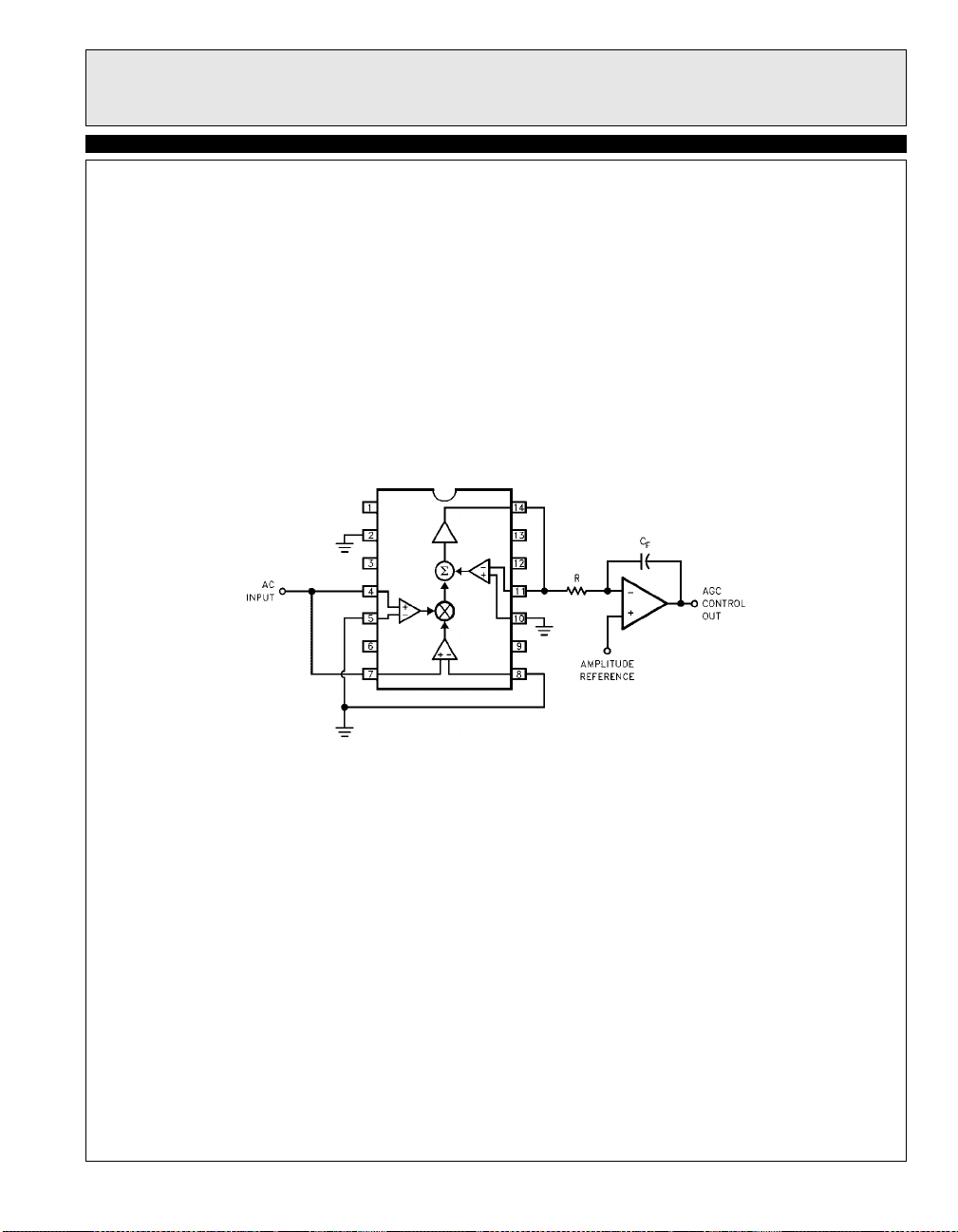
AGC detector and control loop would be:
Figure 2. Traditional AGC Detector/DC Feedback Circuit
The EL4450C simply provides an output equal to the
square of the input signal and an integrator filters ou t the
AC component, while comparing the DC component to
an amplitude reference. The integrat or output is the DC
control voltage to the variable-g ain sect ions of th e AGC
(not shown). If a negative polarity of reference is
required, one of the multiplier i nput terminal pairs is
reversed, inverting the multiplier output. In-
put bias current will cause input voltage offs ets due to
source impedances; puttin g a compensati ng resistor in
series with the grounded inputs of the EL445 0C will
reduce this offset greatly.
This control system will attempt to force
VIN,RMS2/4=V
The extra op-amp can be eliminated by using this circuit:
9
REF
.
Page 10
EL4450C
Wideband Four-Quadrant Multiplier
EL4450C
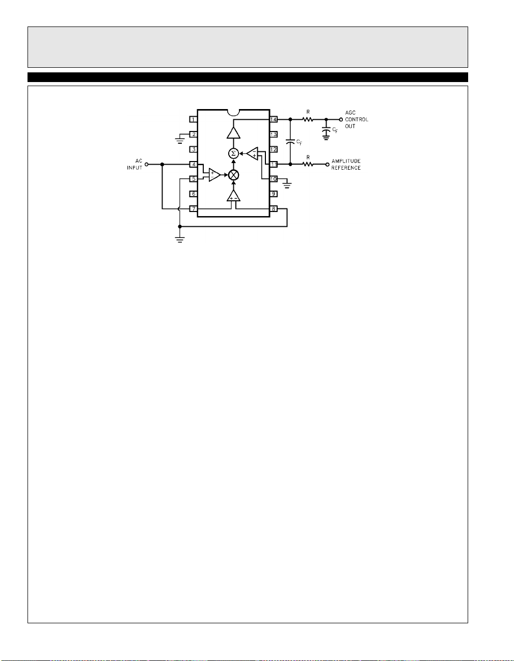
Figure 3. Simplified AGC Detector/DC Feedback Circuit
Here the internal op-amp of the EL4450C replaces the
external amplifier. The feedback capacitor C
provide a perfect integratio n action; a zero occurs at a
frequency of 1/2¼RCF. This is canceled by including
another RC
ence voltage must be negative, the resistor at pin 11 is
connected to ground rather than the reference and pin 10
connected to the reference.
The amplitude reference will have to support some AC
currents flowing through R. If this is a problem, several
changes can be made to
pair at the AGC control output. If the refer-
F
does not
F
eliminate it. The reference is conne cted to p in 10 and the
resistor R connected to pin 11 reconnected to ground,
and one of the multiplier in pu t c onne ctio ns a re reve rse d.
Square-law detectors have a restricted input range, about
10:1, because th e output rap idly di sappears in to the DC
errors as signal amplitudes reduce. This circuit g ives a
multiplier output that is the absolute value of the input,
thus increasing range to 100:1:
10
Page 11
Wideband Four-Quadrant Multiplier
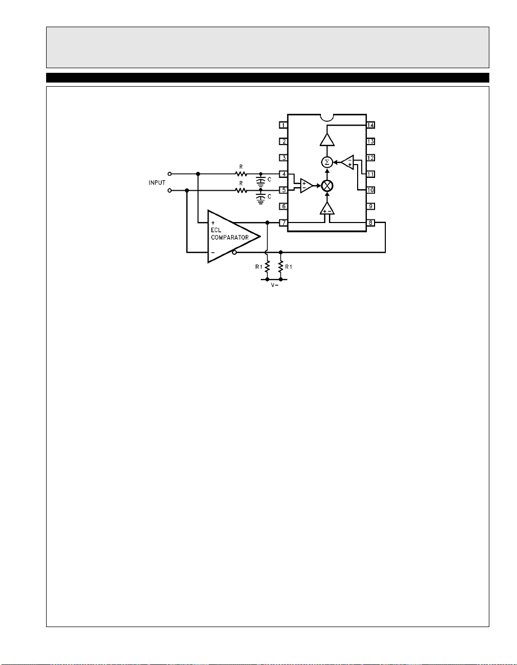
Figure 4. Absolute-Value Input Circuitry
EL4450C
EL4450C
An ECL comparator produces an output corresponding
to the sign of the input, which when multiplied by the
input produces an effective
absolute-value function. The RC product con nected to
the X inputs simply emulates the time delay of the comparator to maintain circuit accuracy at higher
frequencies.
11
Page 12
EL4450C
Wideband Four-Quadrant Multiplier
EL4450C
Nonlinear Function Generation
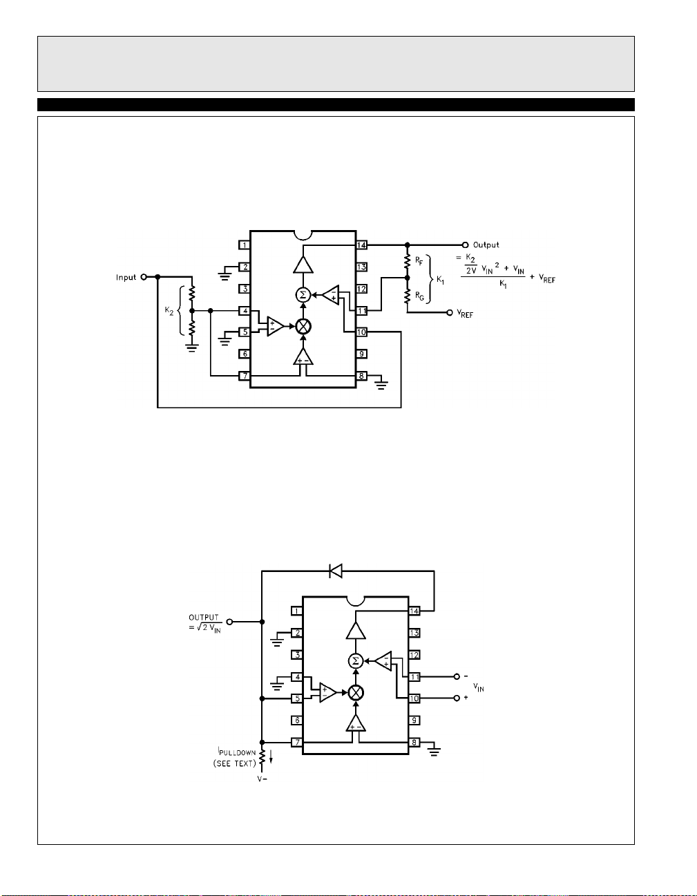
The REF pin of the EL 44 50 C ca n be use d to su m in va rious quantities of polynomial function generators. For
instance, this sum of REF allows a linear signal path
Figure 5. Polynomial Function Generator
which can have various amounts of squared signal
added:
The polarity of the squared signal can be reversed by
swapping one of the X or Y input pairs.
The REF and FB pins also simplify feedback schemes
that allow square-rooting:
Figure 6. Square-Rooter
The diode and I
always produce the positive square-root of the inp ut signal. I
pulldown
diode be forward-biased for any load current. In this
configuration, the band width of t he circuit wi ll reduce
for smaller input signals.
12
pulldown
should be large enough to assure that the
assure that the output will
Page 13
EL4450C
Wideband Four-Quadrant Multiplier
EL4450C
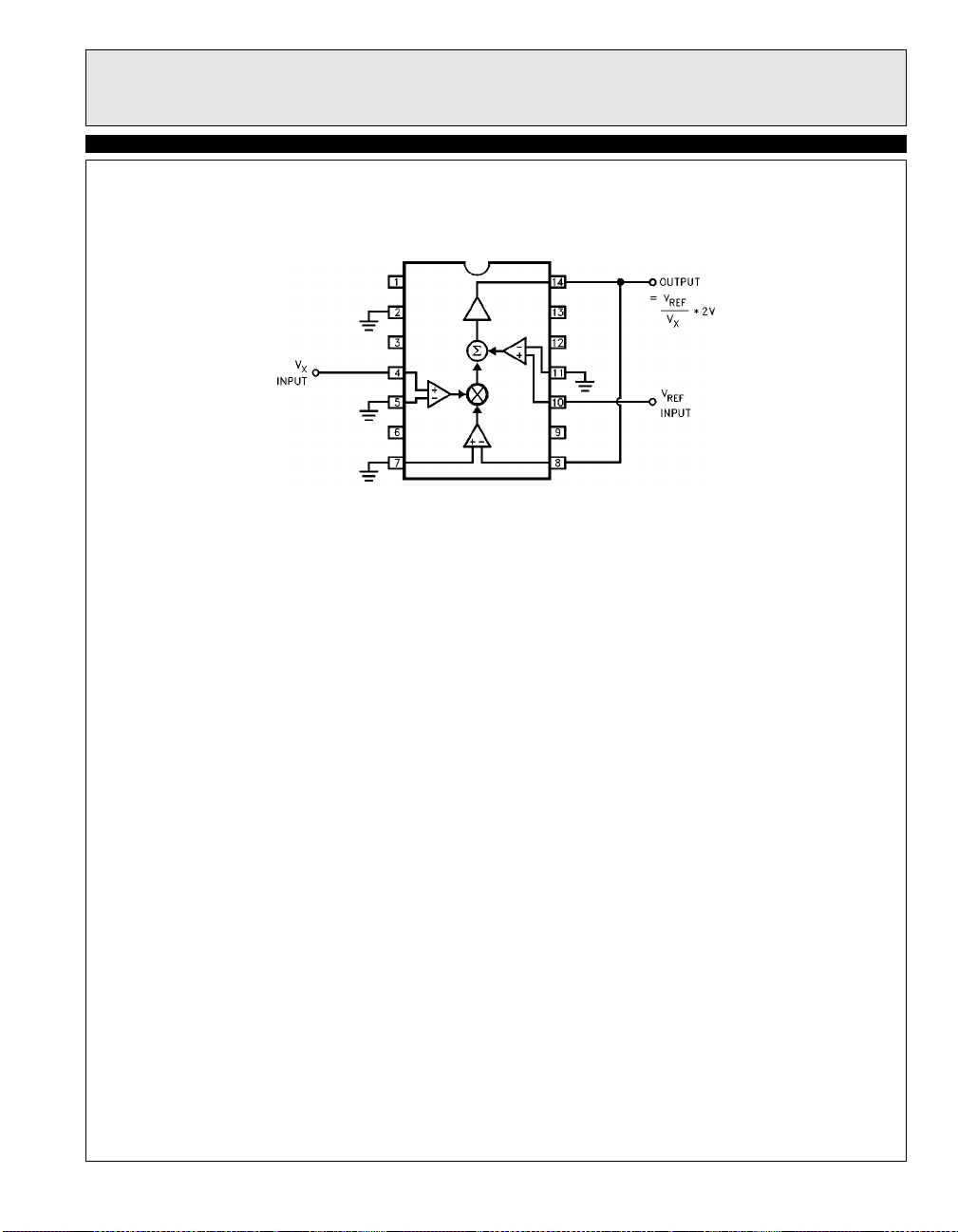
The REF and FB terminals can also be used to implement division:
Figure 7. Divider Connection
The output frequency response reduces for smaller v alues of V
, but is not affected by V
X
REF
.
13
Page 14

EL4450C
Wideband Four-Quadrant Multiplier
EL4450C
General Disclaimer
Specifications contained in this data sheet are in effect as of the publi cation date shown. Elantec, Inc. reserves t he right to make changes i n the cir cuitry or specifications contained herein at any time wi thout notice. Elantec, Inc. assumes no responsibilit y for th e us e of any circuits described
herein and makes no representations that they are free from patent infringement.
WARNING - Life Support Policy
Elantec, Inc. products are not authorized for and should not be used
within Life Support Systems without the specific written consent of
Elantec, Inc. Life Support systems are equipment int ended to sup-
Elantec, Inc.
1996 Tarob Cour t
Milpitas, CA 95035
Telephone: (408) 945-1323
(800) 333-6314
Fax: (408) 945-9305
European Office: 44-71-482-4596
port or sustain life and whose failure to perform when properly used
in accordance with instructions provided can be reasonably
expected to result in significant personal injury or death. Users contemplating applic ation of E lantec, Inc . Products in Life Supp ort
Systems are requested to contact Elantec, Inc. factory headquarters
to establish suitable terms & conditions for these applications. Elan-
tec, Inc.’s warranty is limited to replacement of defective
components and does no t cover inj ury to persons or property or
other consequential damages.
January 1996 Rev B
14
Printed in U.S.A.
 Loading...