

Page 1
EL4430C/EL4431C
Video Instrumentation Amplifiers
EL4430C/EL4431C January 1996 Rev. D
Features
# Fully differential inputs and
feedback
Ð Differential input range of
g
2V
Ð Common-mode range of
g
12V
Ð High CMRR at 4 MHz of
70 dB
Ð Stable at gains of 1, 2
# Calibrated and clean input
clipping
# 4430Ð80 MHz
@
Ge1
# 4431Ð160 MHz GBWP
# 380V/ms slew rate
# 0.02% or
differential gain or
§
phase
# Operates on
g
5tog15V
supplies with no AC degradation
Applications
# Line receivers
# ‘‘Loop-through’’ interface
# Level translation
# Magnetic head pre-amplification
# Differential-to-single-ended
conversion
General Description
The EL4430 and 4431 are video instrumentation amplifiers
which are ideal for line receivers, differential-to-single-ended
converters, transducer interfacing, and any situation where a
differential signal must be extracted from a background of common-mode noise or DC offset.
These devices have two differential signal inputs and two differential feedback terminals. The FB terminal connects to the amplifier output, or a divided version of it to increase circuit gain,
and the REF terminal is connected to the output ground or
offset reference.
The EL4430 is compensated to be stable at a gain of 1 or more,
and the EL4431 for a gain of 2 or more.
The amplifiers have an operational temperature of
a
85§C and are packaged in plastic 8-pin DIP and SO-8.
b
40§Cto
The EL4430 and EL4431 are fabricated with Elantec’s proprietary complementary bipolar process which gives excellent signal symmetry and is free from latchup.
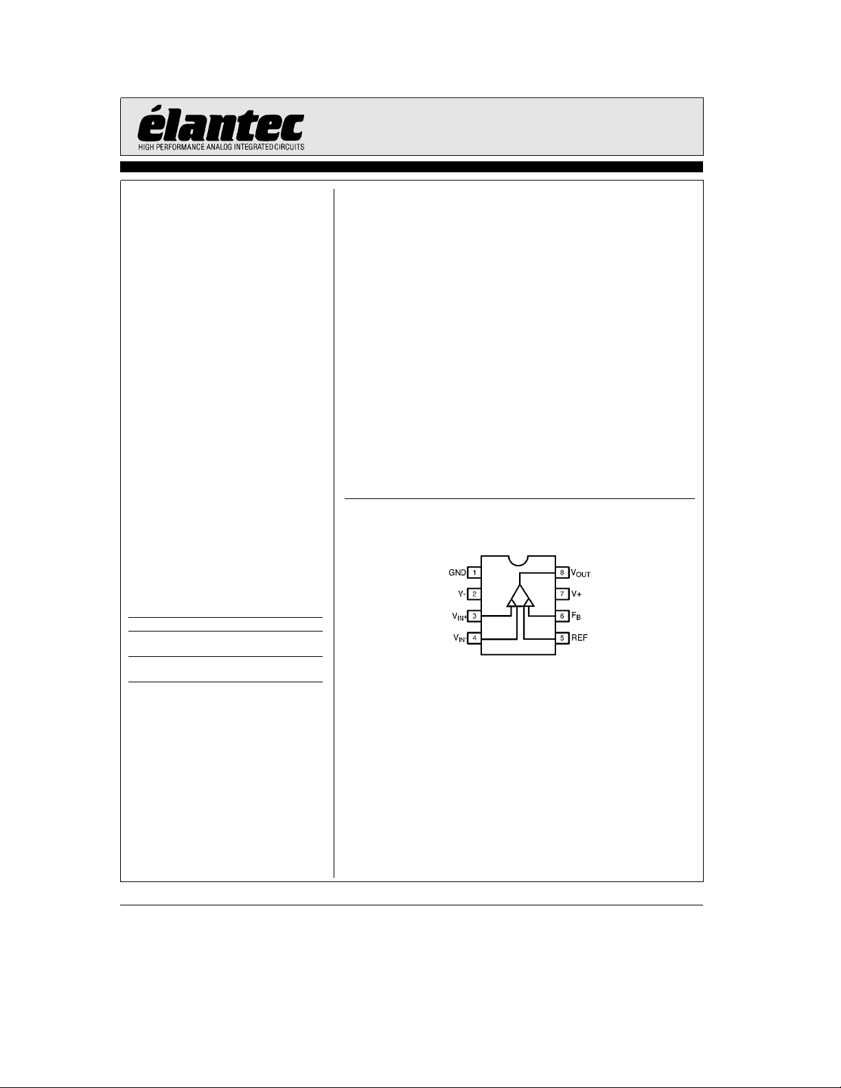
Connection Diagram
Ordering Information
Part No. Temp. Range Package Outline
EL4430CNb40§Ctoa85§C 8-pin P-DIP MDP0031
EL4430CS
EL4431CNb40§Ctoa85§C 8-pin P-DIP MDP0031
EL4431CS
Note: All information contained in this data sheet has been carefully checked and is believed to be accurate as of the date of publication; however, this data sheet cannot be a ‘‘controlled document’’. Current revisions, if any, to these
specifications are maintained at the factory and are available upon your request. We recommend checking the revision level before finalization of your design documentation.
©
1996 Elantec, Inc.
b
40§Ctoa85§C 8-lead SO MDP0027
b
40§Ctoa85§C 8-lead SO MDP0027
Ý
4430– 1
Page 2
EL4430C/EL4431C
Video Instrumentation Amplifiers
Absolute Maximum Ratings
a
Positive Supply Voltage 16.5V
V
V
Vato VbSupply Voltage 33V
S
V
Voltage at any Input or Feedback Vato V
IN
DVINDifference between Pairs
I
IN
Important Note:
All parameters having Min/Max specifications are guaranteed. The Test Level column indicates the specific device testing actually
performed during production and Quality inspection. Elantec performs most electrical tests using modern high-speed automatic test
equipment, specifically the LTX77 Series system. Unless otherwise noted, all tests are pulsed tests, therefore T
Test Level Test Procedure
Open-Loop DC Electrical Characteristics
R
F
of Inputs or Feedback 6V
Current into any Input, or Feedback Pin 4 mA
I 100% production tested and QA sample tested per QA test plan QCX0002.
II 100% production tested at T
III QA sample tested per QA test plan QCX0002.
IV Parameter is guaranteed (but not tested) by Design and Characterization Data.
V Parameter is typical value at T
e
e
R
G
500X.
T
MAX
and T
MIN
A
per QA test plan QCX0002.
Parameter Description Min Typ Max
V
V
V
I
B
I
OS
R
DIFF
CM
OS
IN
Differential input voltage - Clipping EL4430/31 2.0 2.3 I V
e
(V
0)
CM
0.1% nonlinearity EL4430/31 1.8 V V
Common-mode range (V
DIFF
Input offset voltage EL4430/31 2 8 I mV
Input bias current (INa,INb, REF, and FB terminals) 12 20 I mA
Input offset current between INaand IN
and between REF and FB
Input resistance EL4430/31 100 230 I kX
e
(T
25§C)
A
I
OUT
P
D
b
T
A
T
S
e
25§C and QA sample tested at T
e
25§C for information purposes only.
A
e
0) V
e
g
5V
S
e
g
V
15V
S
b
Continuous Output Current 30 mA
Maximum Power Dissipation See Curves
Operating Temperature Range
Storage Temperature Range
e
25§C,
A
Power supplies atg5V, T
g
g
2
g
12
3.0 I V
g
13.0 I V
A
b
40§Ctoa85§C
b
60§Ctoa150§C
e
e
T
TA.
J
C
e
25§. For the EL4431,
Test
Level
Units
0.2 2 I mA
CMRR Common-mode rejection ratio 70 90 I dB
PSRR Power supply rejection ratio EL4430/31 60 V dB
E
G
V
O
I
SC
I
S
Gain error, excluding feedback resistors EL4430/31
Output voltage swing EL4430, V
EL4431, V
e
S
e
g
V
S
e
S
e
g
V
S
Output short-circuit current 40 90 I mA
e
Supply current, V
g
15V 13.5 16 I mA
S
b
g
5V
g
15V
g
g
5V
15Vg12.5g13.0 I V
b
1.5
g
2
g
12
2.5
a
0.2
g
2.8 I V
0.5 I %
12.8 I V
g
3.0 I V
TDis 3.5in
2
Page 3
EL4430C/EL4431C
Video Instrumentation Amplifiers
Closed-Loop AC Electrical Characteristics
the EL4430, R
Parameter Description Min Typ Max
BW,b3dB
BW,g0.1 dB 0.1 dB flatness bandwidth EL4430 20 V MHz
Peaking Frequency response peaking EL4430 0.6 V dB
SR Slew rate, V
V
N
dG Differential gain error, Voffset between EL4430 0.02 V %
di Differential gain error, Voffset between EL4430 0.02 V (§)
T
S
e
150X for the EL4431, C
L
b
3 dB small-signal bandwidth EL4430 82 V MHz
betweenb2V anda2V All 380 V V/ms
OUT
Input-referred noise voltage density EL4430/31 26 V nV/rt-Hz
b
0.7V anda0.7V EL4431, R
b
0.7V anda0.7V EL4431, R
Settling time, to 0.1% from a 4V step EL4430 48 V ns
e
15 pF. For the EL4431, R
L
EL4431 80 V MHz
EL4431 14 V MHz
EL4431 1.0 V dB
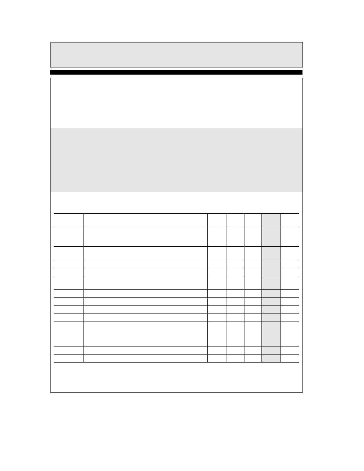
Test Circuit
Power supplies atg12V, T
e
e
R
F
e
L
e
L
500X.
G
150X 0.04 V %
150X 0.08 V (§)
Typical
e
A
25§C, R
Test
Level
e
L
Performance
Curves
EL4430 and EL4431
Common-Mode Rejection
Ratio vs Frequency
500X for
Units
TDis 2.5in
4430– 3
4430– 4
3
Page 4
EL4430C/EL4431C
Video Instrumentation Amplifiers
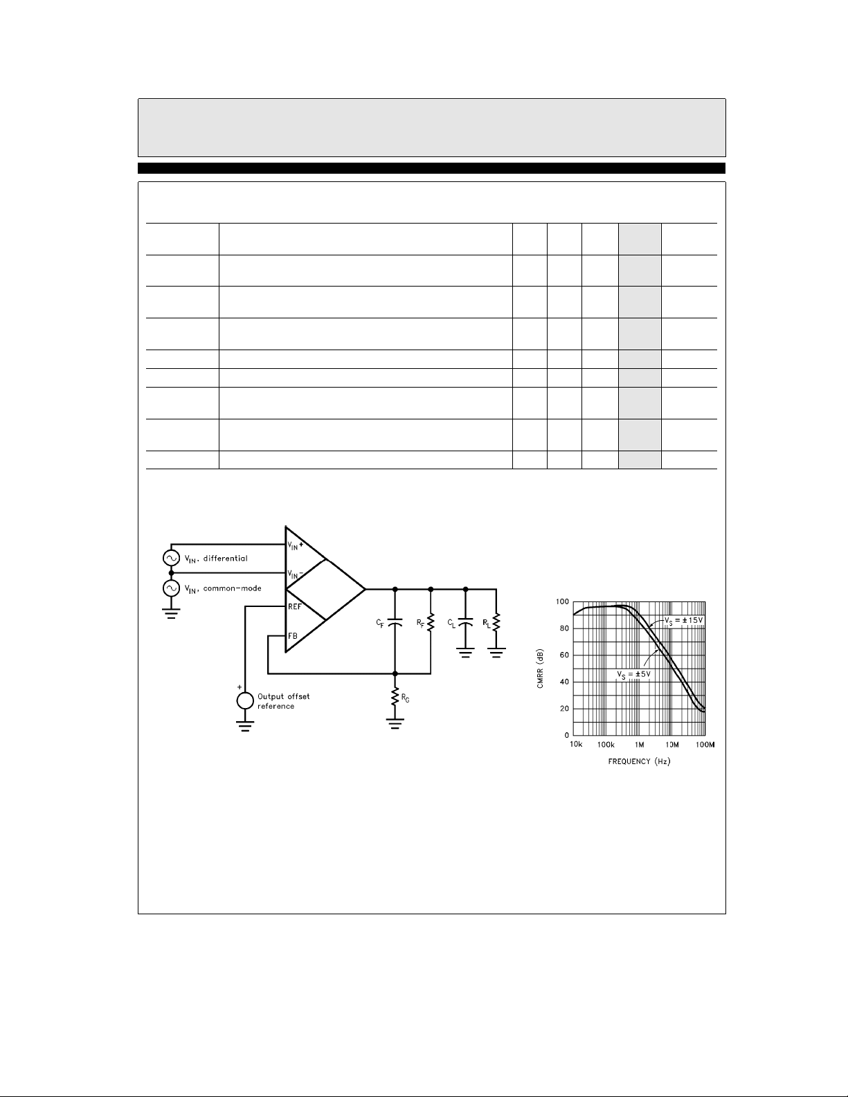
Typical Performance Curves
EL4430 Frequency Response
vs Gain
4430– 5
EL4431 Frequency Response
vs Gain
Ð Contd.
EL4430 Frequency Response
for Various R
e
V
S
EL4431 Frequency Response
for Various R
e
V
S
L,CL
g
5V
L,CL
g
5V
4430– 6
EL4430 Frequency Response
for Various R
e
V
S
EL4431 Frequency Response
for Various R
e
V
S
L,CL
g
15V
4430– 7
L,CL
g
15V
4430– 8
4430– 9
4430– 10
4
Page 5

EL4430C/EL4431C
Video Instrumentation Amplifiers
Typical Performance Curves
EL4430 Differential Gain
and Phase vs Input Offset
Voltage for V
EL4431 Differential Gain
and Phase vs Input Offset
Voltage for V
e
g
5V
S
4430– 14
e
g
5V
S
Ð Contd.
EL4430 Differential Gain
and Phase vs Input Offset
Voltage for V
EL4431 Differential Gain
and Phase vs Input Offset
Voltage for V
e
g
12V
S
e
g
12V
S
4430– 15
EL4430 Differential Gain
and Phase Error vs R
EL4431 Differential Gain
and Phase Error vs R
L
L
4430– 16
4430– 17
EL4430 Nonlinearity
vs Input Signal Span
4430– 20
4430– 18
EL4431 Nonlinearity
vs Input Signal Span
4430– 19
4430– 21
5
Page 6

EL4430C/EL4431C
Video Instrumentation Amplifiers
Typical Performance Curves
EL4430b3 dB Bandwidth
and Peaking vs Supply
Voltage for A
EL4431b3 dB Bandwidth
and Peaking
vs Supply Voltage
V
ea
1
4430– 23
4430– 26
Ð Contd.
EL4430b3 dB Bandwidth
and Peaking vs Die
Temperature for A
EL4431b3 dB Bandwidth
and Peaking vs Die
Temperature for A
V
V
ea
ea
1
4430– 24
2
4430– 27
EL4430 Gain,b3 dB Bandwidth
and Peaking vs Load Resistance
ea
for A
EL4431 Gain,b3 dB Bandwidth
and Peaking vs Load
Resistance for A
1
V
4430– 25
ea
2
V
4430– 28
6
Page 7

EL4430C/EL4431C
Video Instrumentation Amplifiers
Typical Performance Curves
Slew Rate
vs Supply Voltage
4430– 32
Common Mode Input Range
vs Supply Voltage
Ð Contd.
Slew Rate
vs Die Temperature
Offset Voltage
vs Die Temperature
4430– 33
Input Voltage and Current
Noise vs Frequency
4430– 34
Bias Current
vs Die Temperature
Supply Current
vs Supply Voltage
4430– 35
4430– 38
Supply Current
vs Die Temperature
7
4430– 36
4430– 39
Power Dissipation
vs Ambient Temperature
4430– 37
4430– 40
Page 8

EL4430C/EL4431C
Video Instrumentation Amplifiers
Applications Information
The EL4430 and EL4431 are designed to convert
a fully differential input to a single-ended output.
It has two sets of inputs; one which is connected
to the signal and does not respond to its common-mode level, and another which is used to
complete a feedback loop with the output. Here is
a typical connection:
4430– 2
The gain of the feedback divider is H. The transfer function of the part is
c
e
V
OUT
V
is connected to V
FB
network, so V
FB
a
A
O
(V
e
REF
HcV
loop gain of the amplifier, and is about 600 for
the EL4430 and EL4431. The large value of A
drives
(V
IN
a)b
(V
IN
b)a
Rearranging and substituting for V
V
OUT
e
((V
IN
a)b
Thus, the output is equal to the difference of the
V
’s and offset by V
IN
feedback divider ratio. The input impedance of
the FB terminal (equal to R
nals) is in parallel with an R
gain slightly.
The EL4430 is stable for a gain of 1 (a direct
connection between V
the EL4431 for gains of 2 or more. It is important
to keep the feedback divider’s impedance at the
FB terminal low so that stray capacitance does
not diminish the loop’s phase margin. The pole
caused by the parallel of resistors R
a)b
((V
IN
b
OUT
(V
(V
IN
, all gained up by the
REF
and FB) or more and
OUT
(V
IN
VFB)).
through a feedback
OUT.AO
REF
b)a
IN
G
is the open-
b
VFB)x0.
FB
V
REF
of the input termi-
, and raises circuit
and RGand
F
b
)
)/H.
stray capacitance should be at least 200 MHz;
typical strays of 3 pF thus require a feedback impedance of 270X or less. Two 510X resistors are
acceptable for a gain of 2; 300X and 2700X make
a good gain-of-10 divider. Alternatively, a small
capacitor across R
can be used to create more of
F
a frequency-compensated divider. The value of
the capacitor should scale with the parasitic capacitance at the FB terminal input. It is also
practical to place small capacitors across both the
feedback resistors (whose values maintain the desired gain) to swamp out parasitics. For instance,
two 10 pF capacitors (for a gain of 2) across equal
divider resistors will dominate parasitic effects
and allow a higher divider resistance.
Input Connections
The input transistors can be driven from resistive
and capacitive sources, but are capable of oscillation when presented with an inductive input. It
takes about 80nH of series inductance to make
the inputs actually oscillate, equivalent to 4
unshielded wiring or about 6
of unterminated
×
input transmission line. The oscillation has a
characteristic frequency of 500 MHz. Often, placing one’s finger (via a metal probe) or an oscilloscope probe on the input will kill the oscillation.
Normal high-frequency construction obviates
O
any such problems, where the input source is reasonably close to the input. If this is not possible,
one can insert series resistors of approximately
51X to de-Q the inputs.
Signal Amplitudes
Signal input common-mode voltage must be between (V
b)a
3V and (Va)b3V to ensure linearity. Additionally, the differential voltage on any
input stage must be limited to
g
6V to prevent
damage. The differential signal range is
the EL4430 and EL4431. The input range is substantially constant with temperature.
The Ground Pin
The ground pin draws only 6mA maximum DC
current, and may be biased anywhere between
b)a
(V
2.5V and (Va)b3.5V. The ground pin is
connected to the IC’s substrate and frequency
compensation components. It serves as a shield
within the IC and enhances CMRR over frequency, and if connected to a potential other than
ground, it must be bypassed.
g
of
×
2V in
8
Page 9

EL4430C/EL4431C
Video Instrumentation Amplifiers
Applications Information
Ð Contd.
Power Supplies
The instrumentation amplifiers work well on any
supplies from
g
3V tog15. The supplies may be
of different voltages as long as the requirements
of the Gnd pin are observed ( see the Ground Pin
section for a discussion). The supplies should be
bypassed close to the device with short leads.
4.7mF tantalum capacitors are very good, and no
smaller bypasses need be placed in parallel. Capacitors as low as 0.01mF can be used if small
load currents flow.
Single-polarity supplies, such as
a
5V can be used, where the ground pin is con-
nected to
a
5V and V- to ground. The inputs and
a
12V with
outputs will have to have their levels shifted
above ground to accommodate the lack of negative supply.
The dissipation of the amplifiers increases with
power supply voltage, and this must be compatible with the package chosen. This is a close estimate for the dissipation of a circuit:
e
P
2cV
D
c
S
VO/R
c
IS, maxa(V
PAR
b
VO)
S
where IS, max is the maximum supply current
V
is thegsupply voltage
S
(assumed equal)
V
is the output voltage
O
R
is the parallel of all resistors
PAR
loading the output
The maximum dissipation a package can offer is
, maxe(TJ, maxbTAmax)/i
P
D
JA
where TJ, max is the maximum die junction
temperature, 150
C for reliability, less to
§
retain optimum electrical performance.
T
, max is the ambient temperature, 70§C
A
for commercial and 85
C for industrial
§
range.
i
is the thermal resistance of the
JA
mounted package, obtained from datasheet dissipation curves.
The more difficult case is the SO-8 package. With
a maximum die temperature of 150
mum ambient temperature of 85
C and a maxi-
§
C, the 65§C tem-
§
perature rise and package thermal resistance of
170
C/W gives a dissipation of 382 mW at 85§C.
§
This allows a maximum supply voltage of
g
8.5V
for the EL4431 operated in our example. If an
EL4430 were driving a light load (R
it could operate on
g
15V supplies at a 70§C max-
PAR
x
%
imum ambient.
Output Loading
The output stage of the instrumentation amplifiers is very powerful. It typically can source
80 mA and sink 120 mA. Of course, this is too
much current to sustain and the part will eventually be destroyed by excessive dissipation or by
metal traces on the die opening. The metal traces
are completely reliable while delivering the
30 mA continuous output given in the Absolute
Maximum Ratings table in this datasheet, or
higher purely transient currents.
),
For instance, the EL4431 draws a maximum of
16 mA and we might require a 2V peak output
into 150X and a 270X
The R
is 117X. The dissipation withg5V
PAR
a
270X feedback divider.
supplies is 201 mW. The maximum supply voltage that the device can run on for a given P
and
D
the other parameter is
V
, maxe(P
S
(2I
a
VO2/R
D
a
VO/R
S
PAR
PAR
)/
)
Gain or gain accuracy degrades only 10% from
no load to 100X load. Heavy resistive loading will
degrade frequency response and video distortion
for loads
k
100X
Capacitive loads will cause peaking in the frequency response. If capacitive loads must be driven, a small-valued series resistor can be used to
isolate it (12X to 51X should suffice). A 22X series resistor will limit peaking to 2.5 dB with
even a 220 pF load.
9
Page 10

EL4430C/EL4431C
Video Instrumentation Amplifiers
* Macromodel
* This is a Pspice-compatible macromodel of the EL4430 video instrumentation
* amplifier assembled as a subcircuit. The pins are numbered sequentially
* as the subcircuit interface nodes. T1 is a transmission line which provides
* a good emulation of the more complicated real device. This model correctly
* displays the characteristics of input clipping, frequency response, CMRR
* both AC and DC, output clipping, output sensitivity to capacitive loads,
* gain accuracy, slewrate limiting, input bias current and impedance. The
* macromodel does not exhibit proper results with respect to supply current,
* supply sensitivities, offsets, output current limit, differential gain or
* phase, nor temperature.
* Connections: IN
.SUBCKT EL4430/EL 3 4 2 7 6 5 8 1
***
*** EL4430 macromodel ***
***
******
i1 7 10 .00103
i2 7 11 .00103
i3 7 12 .00105
i4 7 13 .00105
v17143
v27153
v3 19 2 3
******
c1 11 1 .03p
c2 12 1 .03p
c3 18 1 2.1p
c4 16 17 0.6p
******
r1 10 11 2000
r2 12 13 2000
r3 10 1 30e6
r4 16 2 1000
r5 17 2 1000
r6 18 1 1.27e6
r7 23 21 20
r8 21 8 100
******
11 21 8 50n
******
d1 11 14 diode
d2 12 14 diode
d3 18 15 diode
d4 19 18 diode
.model diode d(tt
******
q1 16 3 10 1 pnp
q2 17 4 11 1 pnp
q3 16 5 12 1 pnp
q4 17 6 13 1 pnp
.model pnp pnp (bf
******
g1 18 1 17 16 .0005
e12011181.0
t1221201z0
r1t1 22 1 50
e2 23 1 22 1 1.0
******
.ENDS
e
e
50 tde1.5n
a
l
ll
lll
llll
lllll
llllll
llllll l
llllll l l
120n)
e
90 vae44 tre50n)
VIN
b
b
V
a
V
VFB
VREF
VOUT
GND
TDis 7.0in
10
Page 11

EL4430C/EL4431C
Video Instrumentation Amplifiers
EL4430C/EL4431C Macromodel
Ð Contd.
4430– 41
11
Page 12

EL4430C/EL4431C
Video Instrumentation Amplifiers
EL4430C/EL4431CJanuary 1996 Rev. D
General Disclaimer
Specifications contained in this data sheet are in effect as of the publication date shown. Elantec, Inc. reserves the right to make changes
in the circuitry or specifications contained herein at any time without notice. Elantec, Inc. assumes no responsibility for the use of any
circuits described herein and makes no representations that they are free from patent infringement.
WARNING Ð Life Support Policy
Elantec, Inc. products are not authorized for and should not be
used within Life Support Systems without the specific written
consent of Elantec, Inc. Life Support systems are equipment in-
Elantec, Inc.
1996 Tarob Court
Milpitas, CA 95035
Telephone: (408) 945-1323
(800) 333-6314
Fax: (408) 945-9305
European Office: 44-71-482-4596
tended to support or sustain life and whose failure to perform
when properly used in accordance with instructions provided can
be reasonably expected to result in significant personal injury or
death. Users contemplating application of Elantec, Inc. products
in Life Support Systems are requested to contact Elantec, Inc.
factory headquarters to establish suitable terms & conditions for
these applications. Elantec, Inc.’s warranty is limited to replacement of defective components and does not cover injury to persons or property or other consequential damages.
Printed in U.S.A.12
 Loading...