

Page 1
EL4421C/22C/41C/42C/43C/44C
Multiplexed-Input Video Amplifiers
EL4421C/22C/41C/42C/43C/44C January 1996 Rev C
Features
# Unity ora2-gain bandwidth of
80 MHz
# 70 dB off-channel isolation at
4 MHz
# Directly drives high-impedance
or 75X loads
# .02% and .02
differential gain
§
and phase errors
# 8 ns switching time
k
#
100 mV switching glitch
# 0.2% loaded gain error
# Compatible with
g
3V tog15V
supplies
# 160 mW maximum dissipation at
g
5V supplies
Ordering Information
Part No. Temp. Range Package Outline
EL4421CNb40§Ctoa85§C 8-Pin PDIP MDP0031
EL4421CS
EL4422CN
EL4422CS
EL4441CNb40§Ctoa85§C 14-Pin PDIP MDP0031
EL4441CS
EL4442CN
EL4442CS
EL4443CNb40§Ctoa85§C 14-Pin PDIP MDP0031
EL4443CS
EL4444CN
EL4444CS
b
40§Ctoa85§C 8-Pin SO MDP0027
b
40§Ctoa85§C 8-Pin PDIP MDP0031
b
40§Ctoa85§C 8-Pin SO MDP0027
b
40§Ctoa85§C 14-Pin SO MDP0027
b
40§Ctoa85§C 14-Pin PDIP MDP0031
b
40§Ctoa85§C 14-Pin SO MDP0027
b
40§Ctoa85§C 14-Pin SO MDP0027
b
40§Ctoa85§C 14-Pin PDIP MDP0031
b
40§Ctoa85§C 14-Pin SO MDP0027
General Description
The EL44XX family of video multiplexed-amplifiers offers a
very quick 8 ns switching time and low glitch along with very
low video distortion. The amplifiers have good gain accuracy
even when driving low-impedance loads. To save power, the amplifiers do not require heavy loading to remain stable.
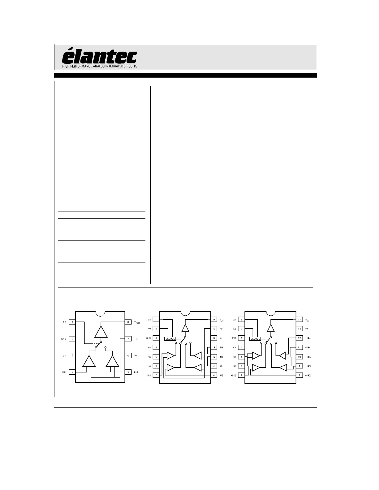
The EL4421 and EL4422 are two-input multiplexed amplifiers.
The -inputs of the input stages are wired together and the device can be used as a pin-compatible upgrade from the
MAX453.
The EL4441 and EL4442 have four inputs, also with common
feedback. These may be used as upgrades of the MAX454.
The EL4443 and EL4444 are also 4-input multiplexed amplifiers, but both positive and negative inputs are wired separately.
A wide variety of gain- and phase-switching circuits can be built
using independent feedback paths for each channel.
The EL4421, EL4441, and EL4443 are internally compensated
for unity-gain operation. The EL4422, EL4442, and EL4444 are
compensated for gains of
ing back-matched cables.
The amplifiers have an operational temperature of
a
85§C and are packaged in plastic 8- and 14-pin DIP and 8- and
14-pin SO.
The EL44XX multiplexed-amplifier family is fabricated with
Elantec’s proprietary complementary bipolar process which
gives excellent signal symmetry and is very rugged.
a
2 or more, especially useful for driv-
b
40§Cto
Connection Diagrams
EL4421/EL4422
4421– 1
Manufactured under U.S. Patent No. 5,352,987
Note: All information contained in this data sheet has been carefully checked and is believed to be accurate as of the date of publication; however, this data sheet cannot be a ‘‘controlled document’’. Current revisions, if any, to these
specifications are maintained at the factory and are available upon your request. We recommend checking the revision level before finalization of your design documentation.
©
1994 Elantec, Inc.
EL4441/EL4442
4421– 2
EL4443/EL4444
4421– 3
Page 2
EL4421C/22C/41C/42C/43C/44C
Multiplexed-Input Video Amplifiers
Absolute Maximum Ratings
a
V
V
S
V
IN
DV
Important Note:
All parameters having Min/Max specifications are guaranteed. The Test Level column indicates the specific device testing actually
performed during production and Quality inspection. Elantec performs most electrical tests using modern high-speed automatic test
equipment, specifically the LTX77 Series system. Unless otherwise noted, all tests are pulsed tests, therefore T
Test Level Test Procedure
Positive Supply Voltage 16.5V
Vato VbSupply Voltage 33V
Voltage at any Input or Feedback Vato V
Difference between Pairs of
IN
Inputs or Feedback 6V
I 100% production tested and QA sample tested per QA test plan QCX0002.
II 100% production tested at T
III QA sample tested per QA test plan QCX0002.
IV Parameter is guaranteed (but not tested) by Design and Characterization Data.
V Parameter is typical value at T
T
MAX
and T
per QA test plan QCX0002.
MIN
e
25§C and QA sample tested at T
A
e
25§C for information purposes only.
A
V
LOGIC
I
IN
b
I
OUT
P
D
Voltage at A0 or A1
Current into any Input, 4 mA
Feedback, or Logic Pin
Output Current 30 mA
Maximum Power Dissipation See Curves
J
e
25§C,
A
b
4V to 6V
e
e
T
TA.
C
Open-Loop DC Electrical Characteristics
Power supplies atg5V, T
e
25§C, R
A
Parameter Description Min Typ Max
V
OS
I
B
Input Offset VoltageÊ21,Ê41, andÊ43
Input Bias Current, Positive Inputs Only
of the
21,Ê22,Ê41,Ê42, and All Inputs of
Ê
theÊ43 andÊ44
I
FB
I
OS
E
G
A
VOL
V
IN
Input Bias Currents of Common Feedback
Input Offset Currents of theÊ43 andÊ44 60 350 I nA
Gain Error of theÊ21 andÊ41 andÊ43 0.2 0.6 I %
Open-Loop Gain EL4443 350 500 I V/V
(Note 1) EL4444 500 750 I V/V
Input Signal Range, EL4421 and EL4441
(Note 2)
CMRR Common-Mode Rejection Ratio, EL4443 70 90 I dB
and EL4444
PSRR Power Supply Rejection Ratio
V
fromg5V tog15V
s
e
500X, unless otherwise specified
L
b
9
22,Ê42, andÊ44
Ê
b
21 andÊ22
Ê
b
41 andÊ42
Ê
22,Ê42 andÊ44(Note 1) 0.1 0.6 I V/V
Ê
b
7
b
12
b
24
b
48
g
2.5
g
39 I
g
27 I
b
50 I mA
b
10 0 I mA
b
20 0 I mA
g
3IV
60 70 I dB
Test
Level
Units
mV
TDis 3.3in
2
Page 3
EL4421C/22C/41C/42C/43C/44C
Multiplexed-Input Video Amplifiers
Open-Loop DC Electrical Characteristics
Power supplies atg5V, T
Parameter Description Min Typ Max
CMIR Common-Mode Input Range
V
OUT
I
SC
F
T
I
LOGIC
V
LOGIC
I
S
Note 1: TheÊ21,Ê41, andÊ43 devices are connected for unity-gain operation with 75X load and an input span ofg1V. TheÊ22,Ê42,
Note 2: The
44 devices are connected for a gain ofa2 with a 150X load and ag1V input span with R
and
Ê
21 andÊ41 devices are connected for unity gain with ag3V input span while the output swing is measured.
Ê
e
25§C
A
(Note 3) EL4443 and EL4444
Output Swing
Output Short-Circuit Current
Unselected Channel Feedthrough ’21, ’41, ’43 70 80 I dB
Attenuation, (Note 1) ’22, ’42, ’44 55 64 I dB
Input Current at A0 and A1
e
with Input
0V and 5V
Logic Valid High and Low Input Levels 0.8 2.0 I V
Supply Current EL4421 and EL4422 11 14
EL4441, EL4442, EL4443, and EL4444 13 16
Ð Contd.
g
2.5
g
2.5
g
40
b
16
Test
Level
g
3IV
g
3.5 I V
g
80 I mA
b
80 I mA
Units
ImA
e
e
R
F
270X.
G
Note 3: CMIR is assured by passing the CMRR test at input voltage extremes.
Closed-Loop AC Electrical Characteristics
Power supplies atg5V. T
ea
2 and R
A
V
L
A
e
150X with R
e
25§C, for EL4421, EL4441, and EL4443 A
e
e
R
G
270X and C
F
e
F
3 pF; for all C
Parameter Description Min Typ Max
BWb3dB
b
3 dB Small-Signal Bandwidth, EL4421, ’41, ’43 80 V MHz
EL4422, ’42, ’44 65 V MHz
BWg0.1 dB 0.1 dB Flatness Bandwidth 10 V MHz
Peaking Frequency Response Peaking 0.5 V dB
SR Slewrate, V
EL4421, EL4441, EL4443 150 200 I V/msec
betweenb2.5V anda2.5V, V
OUT
EL4422, EL4442, EL4444 180 240 I V/msec
V
n
Input-Referred Noise Voltage Density
EL4421, EL4441, EL4443 18 V nV/rt-hz
EL4422, EL4442, EL4444 14 V nV/rt-hz
d
G
Differential Gain Error, V
EL4421, EL4441, EL4443 (V
EL4421, EL4441, EL4443 (V
EL4422, EL4442, EL4444 (V
EL4422, EL4442, EL4444 (V
betweenb0.7V anda0.7V
OFFSET
e
g
12V) 0.01 V %
S
e
g
5V) 0.10 V %
S
e
g
12V) 0.02 V %
S
e
g
5V) 0.11 V %
S
ea
1 and R
V
L
e
g
12V
S
e
e
500X, for EL4422, EL4442, and EL4444
L
15 pF
Test
Level
Units
TDis 2.2inTDis 2.6in
3
Page 4
EL4421C/22C/41C/42C/43C/44C
Multiplexed-Input Video Amplifiers
Closed-Loop AC Electrical Characteristics
Power supplies atg5V. T
ea
A
2 and R
V
L
A
e
150X with R
e
25§C, for EL4421, EL4441, and EL4443 A
e
e
R
G
270X and C
F
F
e
Parameter Description Min Typ Max
d
T
O
MUX
Differential Phase Error, V
EL4421, EL4441, EL4443 (V
EL4421, EL4441, EL4443 (V
EL4422, EL4442, EL4444 (V
EL4422, EL4442, EL4444 (V
betweenb0.7V anda0.7V
OFFSET
e
g
12V) 0.01 V
S
e
g
5V) 0.1 V
S
e
g
12V) 0.02 V
S
e
g
5V) 0.15 V
S
Multiplex Delay Time, Logic Threshold to 50% Signal Change
EL4421, ’22 8 V nsec
EL4441, ’42, ’43, ’44 12 V nsec
V
GLITCH
Peak Multiplex Glitch
EL4421, ’22 70 V mV
EL4441, ’42, ’43, ’44 100 V mV
ISO Channel Off Isolation at 3.58 MHz (See Text)
EL4421, EL4441, EL4443 76 V dB
EL4422, EL4442, EL4444 63 V dB
ea
1 and R
V
3 pF; for all C
e
500X, for EL4422, EL4442, and EL4444
L
e
15 pF Ð Contd.
L
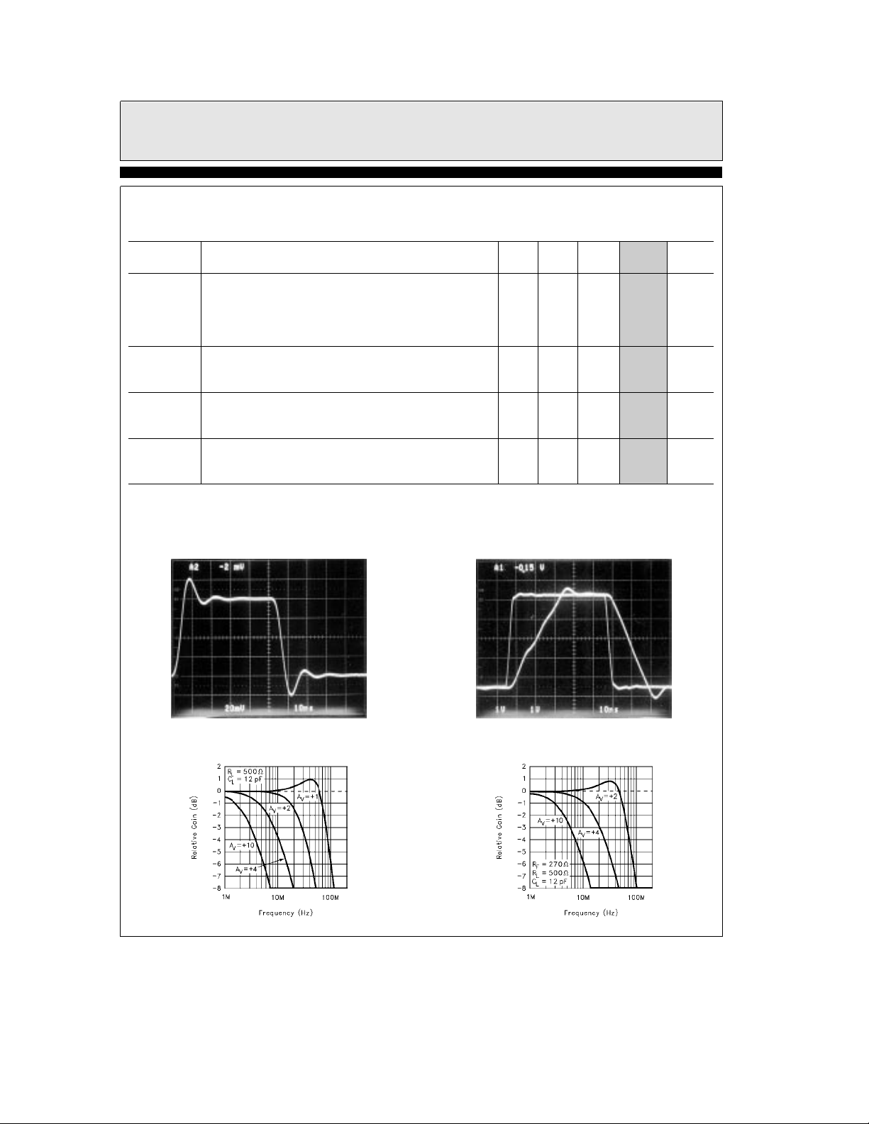
Typical Performance Curves
EL4421, EL4441, and EL4443
Small-Signal Transient Response
e
V
S
g
5V, R
e
500X
L
EL4421, EL4441, and EL4443
Large-Signal Response
e
g
V
S
12V, R
e
500X
L
Test
Level
Units
§
§
§
§
TDis 2.4in
EL4421, EL4441, and EL4443
Frequency Response for
Various Gains
4421– 5
4421– 7
EL4422, EL4442, and EL4444
Frequency Response for
Various Gains
4421– 6
4421– 8
4
Page 5
EL4421C/22C/41C/42C/43C/44C
Multiplexed-Input Video Amplifiers
Typical Performance Curves
EL4421, EL4441, and EL4443
Frequency Response for Various Loads
e
V
S
Frequency Response
for Various Loads
e
V
S
g
g
5V, A
15V, A
V
ea
ea
V
1
1
Ð Contd.
4421– 9
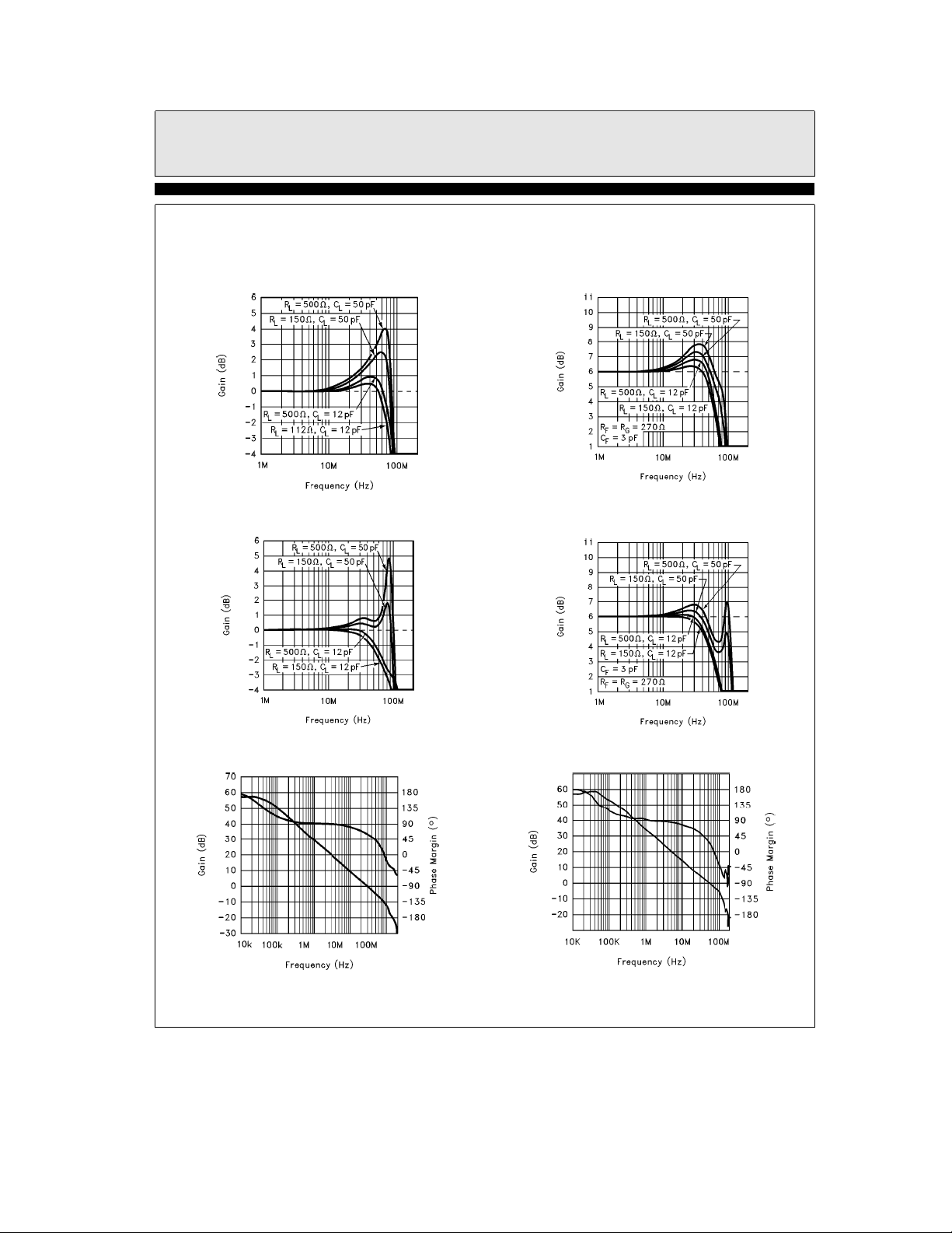
EL4422, EL4442, and EL4444
Frequency Response for Various Loads
e
V
S
EL4422, EL4442, and EL4444
Frequency Response for Various Loads
e
V
S
g
5V, A
g
15V, A
V
ea
V
ea
2
4421– 10
2
EL4443 Open-Loop Gain and
Phase vs Frequency
4421– 11
4421– 13
4421– 12
EL4444 Open-Loop Gain and
Phase vs Frequency
4421– 37
5
Page 6

EL4421C/22C/41C/42C/43C/44C
Multiplexed-Input Video Amplifiers
Typical Performance Curves
EL4421, EL4441, and EL4443
b
3 dB Bandwidth, Slewrate,
and Peaking vs Supply Voltage
EL4421, EL4441, and EL4443
Bandwidth, Slewrate, and Peaking
vs Temperature, A
ea
e
1, R
V
500X
L
Ð Contd.
4421– 14
EL4422, EL4442, and EL4444
b
3 dB Bandwidth, Slewrate,
and Peaking vs Supply Voltage
EL4422, EL4442, and EL4444 Bandwidth,
Slewrate, and Peaking vs Temperature,
ea
e
A
2, R
V
L
150X,R
e
R
I
G
e
270X,C
4421– 15
e
F
3pF
EL4421, EL4441, and EL4443
b
3 dB Bandwidth and Gain Error
vs Load Resistance
4421– 16
4421– 18
4421– 17
Input Noise vs Frequency
4421– 19
6
Page 7

EL4421C/22C/41C/42C/43C/44C
Multiplexed-Input Video Amplifiers
Typical Performance Curves
EL4421, EL4441, and EL4443 Differential Gain
and Phase Errors, vs Input Offset,
ea
A
V
e
1, R
500X,Fe3.58 MHz
L
EL4421, EL4441, and EL4443 Differential Gain
and Phase Error vs Load Resistance;
ea
A
V
1, Fe3.58 MHz, V
OFFSET
e
Ð Contd.
4421– 20
0x0.714V
EL4422, EL4442, and EL4444 Differential Gain
and Phase Error vs Input Offset;
ea
2, R
e
L
150X,Fe3.58 MHz
A
V
EL4443 and EL4444 Open-Loop Gain
vs Load Resistance
4421– 21
Change in V
with Supply Voltage
OS,AV
, and I
4421– 22
B
4421– 24
Change in V
and AVvs Temperature
OS,IB
,
4421– 23
4421– 25
7
Page 8

EL4421C/22C/41C/42C/43C/44C
Multiplexed-Input Video Amplifiers
Typical Performance Curves
Switching Waveforms
Switching from Grounded Input
to Uncorrelated Sinewave and Back
EL4421, EL4441, and EL4443
Unselected Channel
Feedthrough vs Frequency
Ð Contd.
4421– 26
Channel-to-Channel
Switching Glitch
EL4422, EL4442, and EL4444
Unselected Channel
Feedthrough vs Frequency
4421– 27
4421– 28
EL4443 and EL4444
Input and Output Range vs
Supply Voltage (Output Unloaded)
8
4421– 29
4421– 30
Page 9

EL4421C/22C/41C/42C/43C/44C
Multiplexed-Input Video Amplifiers
Typical Performance Curves
Supply Current vs
Supply Voltage
8-Pin Package
Power Dissipation vs
Ambient Temperature
Ð Contd.
4421– 31
Supply Current vs
Temperature
14-Pin Package
Power Dissipation vs
Ambient Temperature
4421– 32
4421– 33
Applications Information
General Description
The EL44XX family of video mux-amps are composed of two or four input stages whose inputs
are selected and control an output stage. One of
the inputs is active at a time and the circuit behaves as a traditional voltage-feedback op-amp
for that input, rejecting signals present at the unselected inputs. Selection is controlled by one or
two logic inputs.
The EL4421, EL4422, EL4441, and EL4442 have
b
all
inputs wired in parallel, allowing a single
feedback network to set the gain of all inputs.
These devices are wired for positive gains. The
EL4443 and EL4444, on the other hand, have all
a
inputs andbinputs brought out separately so
that the input stage can be wired for independent
gains and gain polarities with separate feedback
networks.
The EL4421, EL4441, and EL4443 are compensated for unity-gain stability, while the EL4422,
EL4442, and EL4444 are compensated for a fedback gain of
a
2, ideal for driving back-terminated cables or maintaining bandwidth at higher
fed-back gains.
9
4421– 34
Page 10

EL4421C/22C/41C/42C/43C/44C
Multiplexed-Input Video Amplifiers
Applications Information
Ð Contd.
Switching Characteristics
The logic inputs work with standard TTL levels
of 0.8V or less for a logic 0 and 2.0V or more for a
logic 1, making them compatible for TTL and
Figure 1. Simplified Logic Input Circuitry
The ground pin draws a maximum DC current of
6 mA, and may be biased anywhere between
b)a
(V
may range from (V
ditionally required to be no more negative than
2.5V and (Va)b3.5V. The logic inputs
b)a
2.5V to Va, and are ad-
CMOS drivers. The ground pin is the logic
threshold biasing reference. The simplified input
circuitry is shown below:
4421– 35
b
V(Gnd pin)
V(Gnd pin)
4V and no more positive than
a
6V.
For example, within these constraints, we can
power the EL44XX’s from
a
5V anda12V with-
out a negative supply by using these connections:
Figure 2. Using the EL44XX Mux Amps witha5V anda12V Supplies
10
4421– 36
Page 11

EL4421C/22C/41C/42C/43C/44C
Multiplexed-Input Video Amplifiers
Applications Information
Ð Contd.
The logic input(s) and ground pin are shifted
2.5V above system ground to correctly bias the
mux-amp. Of course, all the signal inputs and
output will have to be shifted 2.5V above system
ground to ensure proper signal path biasing.
A final caution: the ground pin is also connected
to the IC’s substrate and frequency compensation
components. The ground pin must be returned to
system ground by a short wire or nearby bypass
capacitor. In figure 2, the 22 KX resistors also
serve to isolate the bypassed ground pin from the
a
5V supply noise.
Signal Amplitudes
Signal input and output voltages must be between (V
linearity. Additionally, the differential voltage on
any input stage must be limited to
vent damage. In unity-gain connections, any input could have
would be at
tial limit. Higher-gain circuit applications divide
the output voltage and allow for larger outputs.
For instance, at a gain of
b)a
2.5V and (Va)b2.5V to ensure
g
g
3V applied and the output
g
3V, putting us at our 6V differen-
a
2 the maximum input
6V to pre-
g
is again
3V and the output swing isg6V. The
EL4443 or EL4444 can be wired for inverting
gain with even more amplitude possible.
The output and positive inputs respond to overloading amplitudes correctly; that is, they simply
clamp and remain monotonic with increasing
a
input overdrive. A condition exists, however,
where the
b
input of an active stage is overdriven
by large outputs. This occurs mainly in unitygain connections, and only happens for negative
inputs. The overloaded input cannot control the
feedback loop correctly and the output can become non-monotonic. A typical scenario has the
circuit running on
unity gain, and the input is the maximum
g
5V supplies, connected for
g
3V.
Negative input extremes can cause the output to
jump from
er happen if the input is restricted to
b
3V to aroundb2.3V. This will nev-
g
2.5V,
which is the guaranteed maximum input compliance with
g
5V supplies, and is not a problem
with greater supply voltages. Connecting the
feedback network with a divider will prevent the
overloaded output voltage from being large
enough to overload the
b
input and monotonic
11
Page 12

EL4421C/22C/41C/42C/43C/44C
Multiplexed-Input Video Amplifiers
Applications Information
Ð Contd.
behavior is assured. In any event, keeping signals
within guaranteed compliance limits will assure
freedom from overload problems.
The input and output ranges are substantially
constant with temperature.
Power Supplies
The mux-amps work well on any supplies from
g
3V tog15V. The supplies may be of different
voltages as long as the requirements of the Gnd
pin are observed (see the Switching Characteristics section for a discussion). The supplies should
be bypassed close to the device with short leads.
4.7 mF tantalum capacitors are very good, and no
smaller bypasses need be placed in parallel. Capacitors as small as 0.01 mF can be used if small
load currents flow.
Single-polarity supplies, such as
a
5V can be used as described in the Switching
Characteristics section. The inputs and outputs
will have to have their levels shifted above
ground to accommodate the lack of negative supply.
The dissipation of the mux-amps increases with
power supply voltage, and this must be compatible with the package chosen. This is a close estimate for the dissipation of a circuit:
c
e
P
2V
D
Is,maxa(VS–VO)cVO/R
S
Where Is, max is the maximum supply cur-
rent
V
is the
S
g
supply voltage (as-
sumed equal)
V
if the output voltage
O
R
is the parallel of all resistors
PAR
loading the output
a
12V with
PAR
The maximum dissipation a package support is
, maxe(TD, max-TA, max)/R
P
D
TH
Where TD, max is the maximum die temper-
ature, 150
C for reliability, less to re-
§
tain optimum electrical performance
T
, max is the ambient temperature,
A
70
for commercial and 85§C for indus-
§
trial range
R
is the thermal resistance of the
TH
mounted package, obtained from data
sheet dissipation curves
The most difficult case is the SO-8 package. With
a maximum die temperature of 150
mum ambient temperature of 85
C and a maxi-
§
, the 65§temper-
§
ature rise and package thermal resistance of
170
/W gives a maximum dissipation of 382 mW.
§
This allows a maximum supply voltage of
g
9.2V
for the EL4422 operated in our example. If the
EL4421 were driving a light load (R
it could operate on
g
15V supplies at a 70§maxi-
PAR
x
%
mum ambient.
The EL4441 through EL4444 can operate on
g
12V supplies in the SO package, and all parts
can be powered by
g
15V supplies in DIP pack-
ages.
Output Loading
The output stage of the mux-amp is very powerful, and can source 80 mA and sink 120 mA. Of
course, this is too much current to sustain and
the part will eventually be destroyed by excessive
dissipation or by metal traces on the die opening.
The metal traces are completely reliable while delivering the 30 mA continuous output given in
the Absolute Maximum Ratings table in this
data sheet, or higher purely transient currents.
),
For instance, the EL4422 draws a maximum of
14 mA and we might require a 2V peak output
into 150X and a 270X
The R
is 117X. The dissipation withg5V
PAR
a
270X feedback divider.
supplies is 191 mW. The maximum Supply voltage that the device can run on for a given P
and
D
the other parameter is
2
V
, maxe(P
S
a
V
/R
D
O
)/2IsaVO/R
PAR
PAR
Gain or gain accuracy degrades only 10% from
no load to 100X load. Heavy resistive loading will
degrade frequency response and video distortion
only a bit, becoming noticeably worse for loads
k
100X.
)
12
Page 13

EL4421C/22C/41C/42C/43C/44C
Multiplexed-Input Video Amplifiers
Applications Information
Ð Contd.
Capacitive loads will cause peaking in the frequency response. If capacitive loads must be driven, a small-valued series resistor can be used to
isolate it. 12X to 51X should suffice. A 22X series
resistor will limit peaking to 2.5 dB with even a
220 pF load.
Input Connections
The input transistors can be driven from resistive
and capacitive sources but are capable of oscillation when presented with an inductive input. It
takes about 80 nH of series inductance to make
the inputs actually oscillate, equivalent to four
inches of unshielded wiring or about 6
of unter-
×
minated input transmission line. The oscillation
has a characteristic frequency of 500 MHz.
Often simply placing one’s finger (via a metal
probe) or an oscilloscope probe on the input will
kill the oscillation. Normal high-frequency construction obviates any such problems, where the
input source is reasonably close to the mux-amp
input. If this is not possible, one can insert series
resistors of around 51X to de-Q the inputs.
Feedback Connections
A feedback divider is used to increase circuit
gain, and some precautions should be observed.
The first is that parasitic capacitance at the
put will add phase lag to the feedback path and
increase frequency response peaking or even
cause oscillation. One solution is to choose feedback resistors whose parallel value is low. The
pole frequency of the feedback network should be
maintained above at least 200 MHz. Fora3pF
parasitic, this requires that the feedback divider
have less than 265X impedance, equivalent to
two 510X resistors when a gain of
a
Alternatively, a small capacitor across R
used to create more of a frequency-compensated
divider. The value of the capacitor should match
the parasitic capacitance at the
b
input. It is also
practical to place small capacitors across both the
feedback resistors (whose values maintain the desired gain) to swamp out parasitics. For instance,
two 10 pF capacitors across equal divider resistors will dominate parasitic effects and allow a
higher divider resistance.
b
in-
2 is desired.
can be
F
The other major concern about the divider concerns unselected-channel crosstalk. The differential input impedance of each input stage is
around 200 KX. The unselected input’s signal
sources thus drive current through that input impedance into the feedback divider, inducing an
unwanted output. The gain from unselected input to output, the crosstalk attenuation, if R
R
. In unity-gain connection the feedback resis-
IN
F
tor is 0X and very little crosstalk is induced. For
a gain of
a
2, the crosstalk is aboutb60 dB.
Feedthrough Attenuation
The channels have different crosstalk levels with
different inputs. Here is the typical attenuation
for all combinations of inputs for the mux-amps
at 3.58 MHz:
Feedthrough of EL4441 and EL4443 at 3.58 MHz
In1 In2 In3 In4
00 Selected
Select
Inputs,
A1A0
01b80 dB Selectedb77 dBb90 dB
10b101 dBb76 dB Selectedb66 dB
11b96 dBb84 dBb66 dB Selected
Feedthrough of EL4421 at 3.58 MHz
Channel Select 0 Selected
Input, A0
b
77 dBb90 dBb92 dB
In1 In2
b
1
93 dB Selected
b
88 dB
Switching Glitches
The output of the mux-amps produces a small
‘‘glitch’’ voltage in response to a logic input
change. A peak amplitude of only about 90 mV
occurs, and the transient settles out in 20 ns. The
glitch does not change amplitude with different
gain settings.
With the four-input multiplexers, when two logic
inputs are simultaneously changed, the glitch
amplitude doubles. The increase can be a avoided
by keeping transitions at least 6 ns apart. This
can be accomplished by inserting one gate delay
in one of the two logic inputs when they are truly
synchronous.
/
TDis 0.5in TDis 0.5in
13
Page 14

BLANK
14
Page 15

BLANK
15
Page 16

EL4421C/22C/41C/42C/43C/44C
Multiplexed-Input Video Amplifiers
EL4421C/22C/41C/42C/43C/44CJanuary 1996 Rev C
General Disclaimer
Specifications contained in this data sheet are in effect as of the publication date shown. Elantec, Inc. reserves the right to make changes
in the circuitry or specifications contained herein at any time without notice. Elantec, Inc. assumes no responsibility for the use of any
circuits described herein and makes no representations that they are free from patent infringement.
WARNING Ð Life Support Policy
Elantec, Inc. products are not authorized for and should not be
used within Life Support Systems without the specific written
consent of Elantec, Inc. Life Support systems are equipment in-
Elantec, Inc.
1996 Tarob Court
Milpitas, CA 95035
Telephone: (408) 945-1323
(800) 333-6314
Fax: (408) 945-9305
European Office: 44-71-482-4596
tended to support or sustain life and whose failure to perform
when properly used in accordance with instructions provided can
be reasonably expected to result in significant personal injury or
death. Users contemplating application of Elantec, Inc. products
in Life Support Systems are requested to contact Elantec, Inc.
factory headquarters to establish suitable terms & conditions for
these applications. Elantec, Inc.’s warranty is limited to replacement of defective components and does not cover injury to persons or property or other consequential damages.
Printed in U.S.A.16
 Loading...