

Page 1

EL4393C
Triple 80 MHz Video Amplifier w/Disable
EL4393C January 1996 Rev B
Features
# 80 MHzb3 dB bandwidth for
gains of 1 to 10
# 900 V/ms slew rate
# 10 MHz bandwidth flat to 0.1 dB
# Excellent differential gain and
phase
# TTL/CMOS compatible
# Available in SOL-16
Applications
# RGB drivers
# RGB multiplexers
# RGB gain blocks
# Video gain blocks
# Coax cable driver
# ADC drivers/input multiplexer
Ordering Information
Part No. Temp. Range Package Outline
EL4393CNb40§Ctoa85§C 16-Lead P-DIP MDP0031
EL4393CMb40§Ctoa85§C 16-Lead SOL MDP0027
General Description
The EL4393C is three wideband current-feedback amplifiers optimized for video performance. Each amplifier can drive a load
of 150X at video levels. Each amplifier has a disable capability,
which is controlled by a TTL/CMOS compatible logic signal.
The EL4393C operates on supplies as low as
g
4V up tog15V.
Being a current-feedback design, the bandwidth stays relatively
constant at approximately 80 MHz over the
g
1tog10 gain
range. The EL4393C has been optimized for use with 1300X
feedback resistors at a gain of 2.
When the outputs are disabled, the supply current consumption
drops, by about 4 mA per channel that is disabled. This feature
can be used to reduce power dissipation.
Connection Diagram
Ý
4393– 1
Note: All information contained in this data sheet has been carefully checked and is believed to be accurate as of the date of publication; however, this data sheet cannot be a ‘‘controlled document’’. Current revisions, if any, to these
specifications are maintained at the factory and are available upon your request. We recommend checking the revision level before finalization of your design documentation.
©
1993 Elantec, Inc.
Page 2

EL4393C
Triple 80 MHz Video Amplifier w/Disable
Absolute Maximum Ratings
a
Voltage between V
Voltage at V
Voltage at V
Voltage between V
Current into V
Important Note:
All parameters having Min/Max specifications are guaranteed. The Test Level column indicates the specific device testing actually
performed during production and Quality inspection. Elantec performs most electrical tests using modern high-speed automatic test
equipment, specifically the LTX77 Series system. Unless otherwise noted, all tests are pulsed tests, therefore T
Test Level Test Procedure
I 100% production tested and QA sample tested per QA test plan QCX0002.
II 100% production tested at T
III QA sample tested per QA test plan QCX0002.
IV Parameter is guaranteed (but not tested) by Design and Characterization Data.
V Parameter is typical value at T
S
a
S
b
S
IN
a
or V
IN
and V
a
T
and V
b
IN
MAX
b
S
IN
and T
b
A
per QA test plan QCX0002.
MIN
Open Loop DC Electrical Characteristics
Parameter Description Temp Min Typ Max
V
OS
TCV
OS
a
I
B
b
I
B
b
TCI
B
CMRR Common-Mode Rejection Ratio
b
ICMR I
PSRR Power Supply Rejection Ratio
b
IPSR I
R
OL
R
IN
VININaInput Range
V
O
Input Offset Voltage
Temperature Coefficient of V
a
I
Input Bias Current
IN
b
I
Input Bias Current
IN
Temperature Coefficient of I
(Note 1)
b
Input Common-Mode Current
IN
(Note 1)
(Note 2)
b
Current Supply Rejection
IN
(Note 2)
Transimpedance
INaInput Impedance
Output Voltage Swing;
e
1kX
R
L
e
(T
25§C)
A
a
33V
a
18V
b
18V
g
Internal Power Dissipation See Curves
Operating Ambient Temperature Range
Operating Junction Temperature 150
6V
Storage Temperature Range
5mA
e
25§C and QA sample tested at T
e
25§C for information purposes only.
A
a
25§C2
OS
b
B
Full 50 V mV/§C
a
25§C 0.2 5 I mA
a
25§C1065ImA
Full 25 V nA/§C
a
25§C50 58 I dB
a
25§C38ImA/V
a
25§C50 58 I dB
a
25§C25ImA/V
a
25§C 100 217 I kX
a
25§C2 IMX
a
25§C
a
25§C
e
25§C,
A
Supplies atg15V, Loade1KX
g
15 I mV
g
g
g
13
12
13.5 I V
g
13 I V
b
b
65§Ctoa150§C
e
T
J
C
Test
Level
40§Ctoa85§C
e
TA.
Units
§
C
TDis3.4in
2
Page 3

EL4393C
Triple 80 MHz Video Amplifier w/Disable
Open Loop DC Electrical Characteristics
Parameter Description Temp Min Typ Max
I
SC
I
O, DIS
DIS V
IL
DIS V
IH
DIS I
IL
DIS I
IH
I
CC (en)
I
CC (dis)
I
EE (en)
I
EE (dis)
Note 1: V
CM
Note 2: V
OS
Note 3: Only one output short circuited. Pulse test or use heatsink.
Short-Circuit Current (Note 3)
Output Current when Disabled
Disable Voltage for Logic Low
Disable Voltage for Logic High
Disable Logic Low Input Current
Disable Logic High Input Current
Positive Supply Current all
Channels Enabled
Positive Supply Current all
Channels Disabled
Negative Supply Current all
Channels Enabled
Negative Supply Current all
Channels Disabled
e
g
10V for V
is measured at V
e
g
S
e
g
S
15V.
4.5V and V
e
S
a
25§C40 70 I mA
a
25§C 5 150 I mA
a
25§C 0.8 I V
a
25§C 2.2 I V
a
25§C 3 25 I mA
a
25§C05ImA
a
25§C15 20
a
25§C 6 11 16 I mA
a
25§C13 18
a
25§C4 9 14 I mA
g
16V, both supplies are changed simultaneously.
Closed Loop AC Electrical Characteristics
e
where noted. Rf1 and Rf2
1500X;A
Parameter Description Min Typ Max
e
e
2, T
V
25§C. (See note 8 re: test fixture)
A
Supplies atg15V, Loade1KX Ð Contd.
Test
Level
g
29 I mA
g
28 I mA
Supplies atg15V, Loade150X and 15 pF, except
Test
Level
SR Slew Rate (Note 4) 960 V V/ms
SR Slew Rate w/g5V Supplies (Note 5) 470 IV V/ms
t
s
Settling Time to 1% 5V
5V Step (Note 6) 32 V ns
p-p
BW Bandwidth,b3 dB 80 IV MHz
g
5V Supplies,b3 dB 60 IV MHz
BW Bandwidth,b0.1 dB 16 IV MHz
g
5V Supplies,b0.1 dB 21 IV MHz
Peaking
b
3 dB BW Tests 0.6 IV dB
dG Differential Gain at 3.58 MHz 0.03 V %
g
at
5V Supplies (Note 7) 0.30 V %
di Differential Phase at 3.58 MHz 0.088 V (§)
g
at
5V Supplies (Note 7) 0.096 V (§)
Note 4: R
Note 5:
Note 6: R
Note 7: DC offset from
Note 8: Test fixture was designed to minimize capacitance at the I
e
300X,b5V toa5V swing, SR measured at 20% to 80%.
L
b
2V toa2V swing, SR measured at 20% to 80%.
e
300X.
L
capacitance to ground at this very sensitive pin. See application notes for further details.
b
0.7V througha0.7V AC amplitude is 286 mV
, equivalent to 40 ire.
P-P
a
input. A ‘‘good’’ fixture should have less than 2 pF of stray
N
Units
TDis2.7inTDis2.4in
Units
3
Page 4

EL4393C
Triple 80 MHz Video Amplifier w/Disable
Typical Performance Curves
Gain Flatness vs Rf atg5V Gain Flatness vs Rf atg15V
g
Phase vs Rf at
5V Phase vs Rf atg15V
Gain of 5, 10 vs Various Rf,
g
5V
Rg at
Gain of 5, 10 vs Rf,
Rg atg15V
4393– 3
4
Page 5
EL4393C
Triple 80 MHz Video Amplifier w/Disable
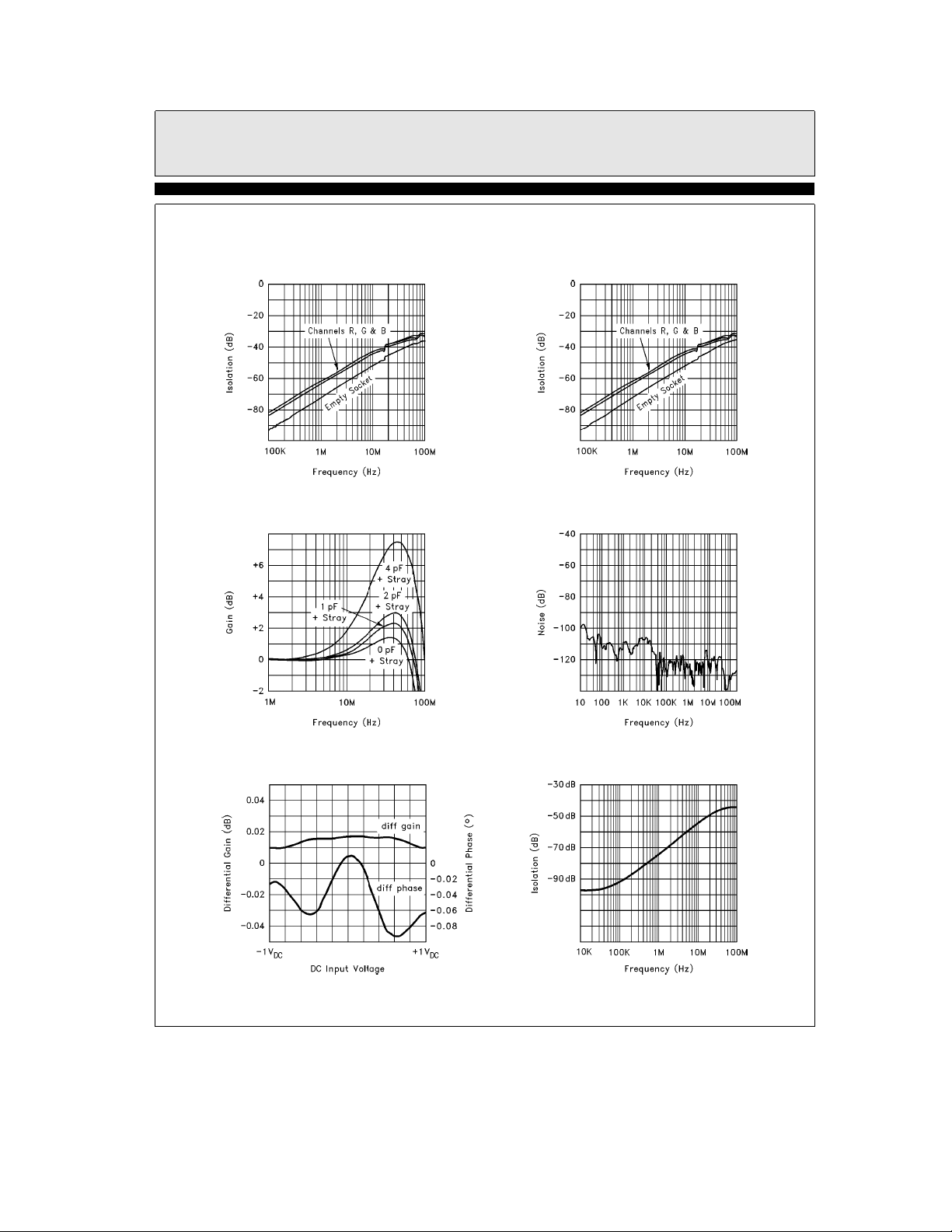
Typical Performance Curves
Disabled
Isolation Test atg5V
CinÐvs Peaking Voltage Noise
Ð Contd.
Disabled
Isolation Test atg15V
Differential Gain & Phase
at 3.58 MHz
EL4393 MUX Channel
Channel Isolation
4393– 11
5
Page 6

EL4393C
Triple 80 MHz Video Amplifier w/Disable
Typical Performance Curves
Supply Current
vs Supply Voltage
Small Signal Pulse Response
Ð Contd.
Maximum Power Dissipation
vs Ambient TemperatureÐ
16-Pin PDIP
Maximum Power Dissipation
vs Ambient TemperatureÐ
16-Pin SOL
Large Signal Pulse Response
4393– 4
Enable/Disable
a
with
VE Voltage Output
4393– 5
4393– 7
4393– 6
Enable/Disable
b
with
VE Voltage Output
4393– 8
6
Page 7

EL4393C
Triple 80 MHz Video Amplifier w/Disable
Typical Application for EL4393,
and General Rules for PCB
Layout
The figure shows two EL4393’s configured as a
2:1 RGB multiplexer, and cable driver, driving
75X, back terminated cables. Each channel of the
EL4393 is configured to give a gain of two, to
make up for the losses of the back terminating
resistor.
In this example, the Disable pins of each RGB
section are driven by a complementary TTL ‘‘select’’ signal. Larger multiplexers can be assembled, with a 1-of-n TTL decoder selecting each
RGB triplet.
The circuit gives channel isolations of typically
better than
dB/decade slope, extending down to better than
b
90 dB at frequencies below 100 kHz.
The schematic does not show things like power
supply decoupling, or pcb layout, grounding and
signal returns, but these will all affect the overall
performance of the circuit, and care should be
taken with these aspects.
b
50 dB at 10 MHz, and with a 20
It is recommended that the V
each be decoupled by a 0.1 mF NPO or X7R dielectric ceramic capacitors to ground within 0.1
inch of the part, and in parallel with the 0.1 mF,
A47mF tantalum capacitor, also to ground. The
47 mF capacitors should be within 0.25 inch of
their power pins. The ground plane should be underneath the package, but cut away from the
b
In
inputs. Care should be taken with the center
channel feedbackÐit must be kept away from
any of the in
the package. Route the G-out line between the
pin 3 ground and the pin 4 In
the package is essential. Otherwise, loop the Gout trace around all the other circuitry, to its Rf
resistor. The Rf and if used, Rg resistors should
be on the input side of the package, to minimize
trace length on the In
The digital input disables are on the output side
of the package, so that a good ground plane down
the center of the board underneath the package
will isolate any fast edges from the sensitive inputs.
a
or inbpins, if it has to go under
b
pins.
and VEEpins
CC
b
if going under
7
Page 8

EL4393C
Triple 80 MHz Video Amplifier w/Disable
Typical Application Circuit
8
4393– 2
Page 9

EL4393C
Triple 80 MHz Video Amplifier w/Disable
EL4393C Macromodel
* Revision A, July 1993
* Enhancements include PSRR, CMRR, and Slew Rate Limiting
* Connections:
*
*
*
*
*
*subckt EL4393/EL 32746
*
*Input Stage
*
e1100301.0
vis 10 9 0V
h2 9 12 vxx 1.0
r121150
l1111229nH
iinp 3 0 0.2 mA
iinm2010mA
*
*Slew Rate Limiting
*
h1 13 0 vis 600
r2 13 14 1K
d1 14 0 dclamp
d2 0 14 dclamp
*
* High Frequency Pole
*
e2 30 0 14 0 0.00166666666
l5 30 17 1.2 mH
c51701pF
r5 17 0 500
*
* Transimpedance Stage
*
g10181701.0
rol 18 0 250k
cdp 18 0 2.2 pF
*
a
input
b
Input
l
ll
lll
llll
a
Vsupply
b
Vsupply
Putput
lllll
* Output Stage
*
q141819qp
q271820qn
q371921qn
q442022qp
r7 21 6 4
r8 22 6 4
ios1 7 19 2.5 mA
ios2 20 4 2.5 mA
*
* Error Terms
*
ivos0232mA
vxx 23 0 0V
e4240301.0
e5250701.0
e6260401.0
r9 24 23 1K
r10 25 23 1K
r11 26 33 1K
*
* Models
*
.model qn npn (is
.model qp pnp (is
.model dclamp d (is
.ends
e5eb
15 bfe100 tfe0.2nS)
e5eb
15 bfe100 tfe0.2nS)
e1eb
30 ibve0.266 bve1.5 ne4)
TABWIDE
TABWIDE
TDis3.6in
TDis5.3in
9
Page 10

EL4393C
Triple 80 MHz Video Amplifier w/Disable
EL4393C Macromodel
Ð Contd.
4393– 9
Simplified Schematic of One Channel of EL4393
10
4393– 10
Page 11

BLANK
11
Page 12

EL4393C
Triple 80 MHz Video Amplifier w/Disable
EL4393CJanuary 1996 Rev B
General Disclaimer
Specifications contained in this data sheet are in effect as of the publication date shown. Elantec, Inc. reserves the right to make changes
in the circuitry or specifications contained herein at any time without notice. Elantec, Inc. assumes no responsibility for the use of any
circuits described herein and makes no representations that they are free from patent infringement.
WARNING Ð Life Support Policy
Elantec, Inc. products are not authorized for and should not be
used within Life Support Systems without the specific written
consent of Elantec, Inc. Life Support systems are equipment in-
Elantec, Inc.
1996 Tarob Court
Milpitas, CA 95035
Telephone: (408) 945-1323
(800) 333-6314
Fax: (408) 945-9305
European Office: 44-71-482-4596
tended to support or sustain life and whose failure to perform
when properly used in accordance with instructions provided can
be reasonably expected to result in significant personal injury or
death. Users contemplating application of Elantec, Inc. products
in Life Support Systems are requested to contact Elantec, Inc.
factory headquarters to establish suitable terms & conditions for
these applications. Elantec, Inc.’s warranty is limited to replacement of defective components and does not cover injury to persons or property or other consequential damages.
Printed in U.S.A.12
 Loading...