

Page 1
EL4390C
Triple 80 MHz Video Amplifier with DC Restore
EL4390C November 1994, Rev A
Features
# 80 MHzb3 dB bandwidth for
gains of 1 to 10
# 800 V/ms slew rate
# 15 MHz bandwidth flat to 0.1 dB
# Excellent differential gain and
phase
# TTL/CMOS compatible DC
restore function
# Available in 16 lead P-DIP, 16
lead SOL
Applications
# RGB drivers requiring DC
restoration
# RGB multiplexers requiring DC
restoration
# RGB building blocks
# Video gain blocks requiring DC
restoration
# Sync and color burst processing
Ordering Information
Part No. Temp. Range Package Outline
EL4390CNb40§Ctoa85§C 16-Pin P-DIP MDP0031
EL4390CMb40§Ctoa85§C 16-Lead SOL MDP0027
General Description
The EL4390C is three wideband current-mode feedback amplifiers optimized for video performance, each with a DC restore
amplifier. The DC restore function is activated by a common
TTL/CMOS compatible control signal while each channel has a
separate restore reference.
Each amplifier can drive a load of 150X at video signal levels.
The EL4390C operates on supplies as low as
g
4V up tog15V.
Being a current-mode feedback design, the bandwidth stays relatively constant at approximately 80MHz over the
gain range. The EL4390C has been optimized for use with
1300X feedback resistors.
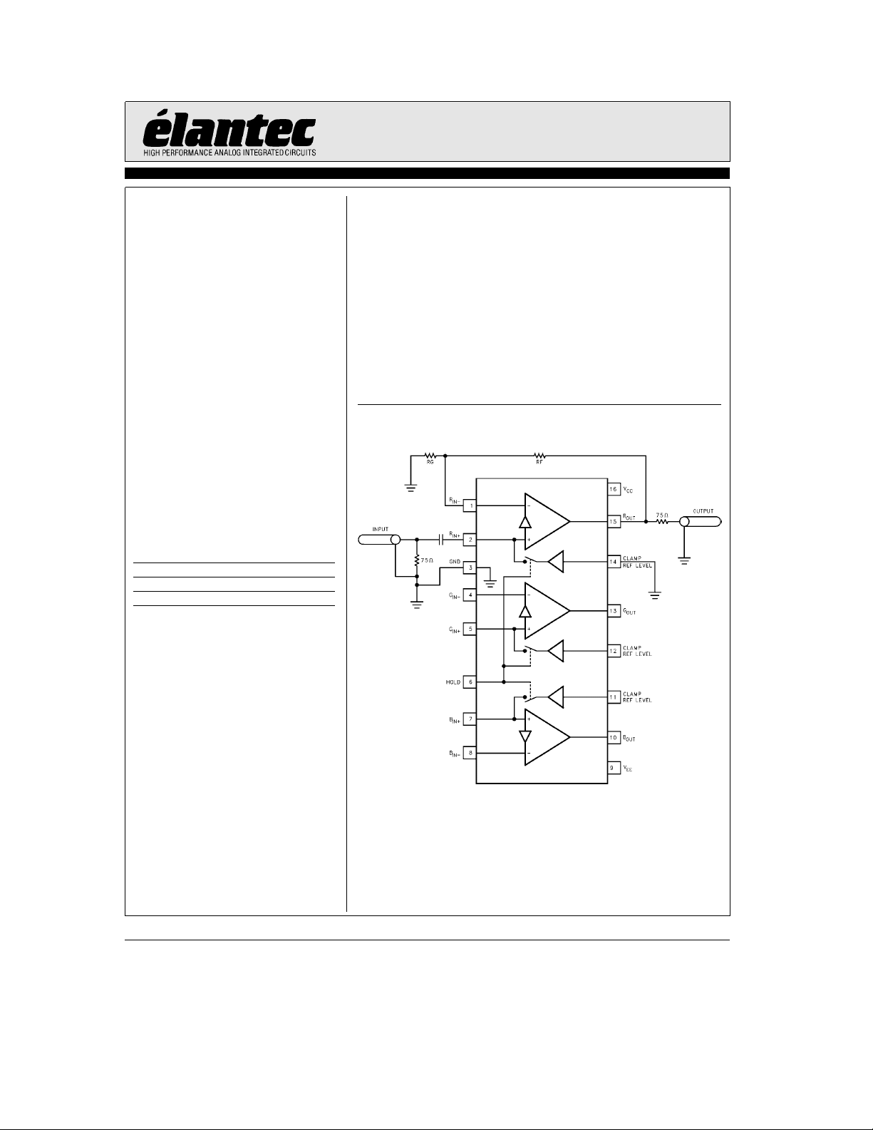
Connection Diagram
Ý
g
1tog10
4390– 1
Note: All information contained in this data sheet has been carefully checked and is believed to be accurate as of the date of publication; however, this data sheet cannot be a ‘‘controlled document’’. Current revisions, if any, to these
specifications are maintained at the factory and are available upon your request. We recommend checking the revision level before finalization of your design documentation.
©
1994 Elantec, Inc.
Page 2

EL4390C
Triple 80 MHz Video Amplifier with DC Restore
Absolute Maximum Ratings
Voltage between V
Voltage at V
Voltage at V
Voltage between V
Current into V
Important Note:
All parameters having Min/Max specifications are guaranteed. The Test Level column indicates the specific device testing actually
performed during production and Quality inspection. Elantec performs most electrical tests using modern high-speed automatic test
equipment, specifically the LTX77 Series system. Unless otherwise noted, all tests are pulsed tests, therefore T
Test Level Test Procedure
I 100% production tested and QA sample tested per QA test plan QCX0002.
II 100% production tested at T
III QA sample tested per QA test plan QCX0002.
IV Parameter is guaranteed (but not tested) by Design and Characterization Data.
V Parameter is typical value at T
a
S
aa
S
bb
S
IN
a
and V
IN
ba
and V
S
a
T
and V
IN
MAX
IN
b
and T
b
A
per QA test plan QCX0002.
MIN
Open Loop DC Electrical Characteristics
Parameter Description Temp Min Typ Max
e
(T
25§C)
A
g
Internal Power Dissipation See Curves
33V
Operating Ambient Temp. Range
18V
Operating Junction Temperature 150
18V
Storage Temperature Range
6V
5mA
e
25§C and QA sample tested at T
e
25§C for information purposes only.
A
e
25§C,
A
Supplies atg15V, Loade1KX
b
40§Ctoa85§C
b
65§Ctoa150§C
e
e
T
J
C
Test
Level
§
TA.
Units
Amplifier Section (not restored)
V
OS
a
I
B
b
I
B
Input Offset Voltage
a
I
Input Bias Current
IN
b
I
Input Bias Current
IN
ROLTransimpedance (Note 1)
b
R
IN
b
I
N
Resistance
CMRR Common-Mode Rejection Ratio (Note 2)
PSRR Power Supply Rejection Ratio (Note 4)
V
O
I
SC
I
SY
Output Voltage Swing; R
Short-Circuit Current
Supply Current (Quiescent)
e
1kX
L
a
25§C 2 15 II mV
a
25§C 0.2 5 II mA
a
25§C1065IImA
a
25§C 100 220 II kX
a
25§C50 VX
a
25§C50 56 II dB
a
25§C50 70 II dB
a
25§C
a
25§C 45 70 100 II mA
a
25§C10 20 32 II mA
g
g
12
13 II V
Restoring Section
VOS, COMP Composite Input Offset Voltage (Note 3)
I
B
I
OUT
a
,
R
Restore I
Restoring Current Available
a
Input Bias Current
N
PSRR Power Supply Rejection Ratio (Note 4)
G
OUT
Conductance
ISY, RES Supply Current, Restoring
VIL, RES RES Logic Low Threshold
VIH, RES RES Logic High Threshold
a
25§C 8 35 II mV
a
25§C 0.2 5 II mA
a
25§C2 4 II mA
a
25§C50 70 II dB
a
25§C 8 V mA/V
a
25§C10 23 37 II mA
a
25§C 1.0 1.4 II V
a
25§C 1.4 1.8 II V
C
TDis4.1in
2
Page 3
EL4390C
Triple 80 MHz Video Amplifier with DC Restore
Open Loop DC Electrical Characteristics
Parameter Description Temp Min Typ Max
Supplies atg15V, Loade1KX Ð Contd.
Test
Level
Restoring Section
IIL, RES RES Input Current, Logic Low
IIH, RES RES Input Current, Logic High
Note 1: For current feedback amplifiers, A
e
g
Note 2: V
Note 3: Measured from V
Note 4: V
10V for V
CM
is measured at V
OS
e
S
to amplifier output, while restoring.
CL
e
S
g
15V.
g
4.5V and V
VOL
e
S
ROL/R
e
a
25§C 2 10 II mA
a
25§C 0.5 3 II mA
b
.
IN
g
16V, both supplies are changed simultaneously.
Closed Loop AC Electrical Characteristics
Supplies atg15V, Loade150X and 15 pF, T
Parameter Description Min Typ Max
Amplifier Section
SR Slew Rate (Note 5) 800 V V/ms
SR Slew Rate w/g5V Supplies (Note 5) 550 V V/ms
BW Bandwidth,b3dB, A
g
5V Supplies,b3dB 72 V MHz
BW Bandwidth,b0.1 dB 20 V MHz
g
5V Supplies,b0.1dB 14 V MHz
dG Differential Gain at 3.58 MHz 0.02 V %
g
at
5V Supplies (Note 6) 0.02 V %
di Differential Phase at 3.58 MHz 0.03 V (§)
g
at
5V Supplies (Note 6) 0.06 V (§)
Restoring Section
T
RE
T
RD
Time to Enable Restore 35 V ns
Time to Disable Restore 35 V ns
Note 5: SR is measured at 20% to 80% of 4V pk-pk square wave, with A
b
Note 6: DC offset from
Note 7: Test fixture was designed to minimize capacitance at the I
capacitance to ground at this very sensitive pin. See application notes for further details.
0.714V toa0.714V, AC amplitude is 286m Vp-p, equivalent to 40 ire.
e
25§C (See note 7 re: test fixture)
A
Test
Level
e
1 95 V MHz
V
e
e
5, R
F
820X,R
V
b
input. A ‘‘good’’ fixture should have less than 2 pF of stray
N
e
200X.
G
Units
TDis0.9inTDis2.7in
Units
3
Page 4
EL4390C
Triple 80 MHz Video Amplifier with DC Restore
Table 1. Charge Storage Capacitor Value vs. Droop and Charging Rates
Cap Value Droop in Charge in Charge in
(nF) 60mS (mV) 2mS (mV) 4mS (mV)
10 30 400 800
22 13.6 182 364
47 6.4 85 170
100 3.0 40 80
220 1.36 18 36
These numbers represent the worst case bias current, and the worst case charging current. Note that to
get the full (2mA
a
) charging current, the clamp input must havel250mV of error voltage.
Note that the magnitude of the bias current will decrease as temperature increases.
The basic droop formula is :
V (droop)
e
c
I
(Line timebCharge time) / capacitor value
a
B
and the basic charging formula is:
V (charge)
Where I
I
OUT
e
is:
OUT
e
(Clamp voltagebINavoltage) / 120
I
OUT
c
Charge time / capacitor value
4
Page 5
Triple 80 MHz Video Amplifier with DC Restore
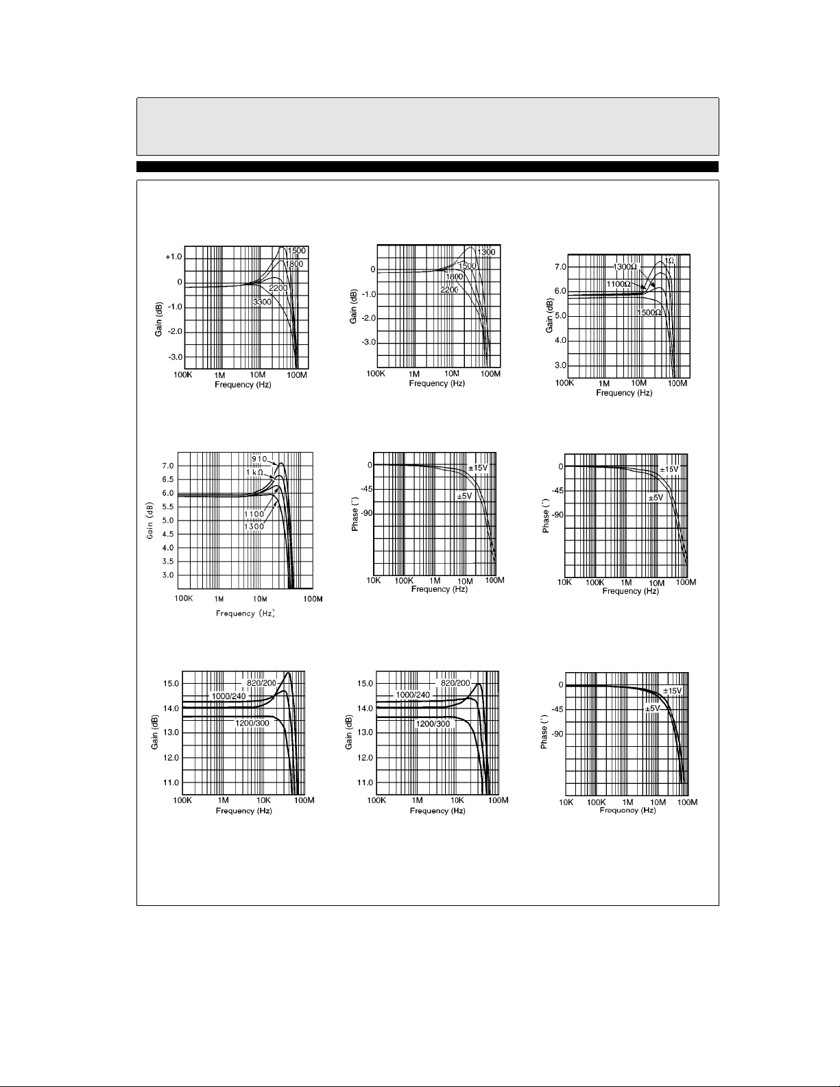
Typical Performance Curves
Gain Flatness
for Various R
e
V
S
g
15V, A
F
e
0dB
V
Gain Flatness
for Various R
e
g
V
5V, A
S
EL4390C
F
e
0dB
V
Gain Flatness
for Various R
e
g
15V, A
V
S
and RGValues
F
e
6dB
V
Gain Flatness
for Various R
e
g
5V, A
V
S
Gain Flatness
e
g
15V, A
V
S
as Shown
R
F/RG
and RGValues
F
e
6dB
V
e
14 dB,
V
4390– 2
4390– 6
Phase Shift
e
e
F
e
S
F/RG
V
R
G
g
5V, A
as Shown
2,
e
for A
R
Gain Flatness
V
R
1300X
V
e
14 dB,
4390– 3
4390– 5
Phase Shift for A
e
e
R
e
S
V
e
200X,V
G
g
e
5 dB, R
1000X
5V and V
S
R
F
at V
Phase Shift
for A
R
G
4390– 4
e
2,
V
e
g
15V
S
4390– 7
e
820X,
F
e
g
5V
4390– 8
4390– 9
4390– 10
5
Page 6

EL4390C
Triple 80 MHz Video Amplifier with DC Restore
Typical Performance Curves
Gain Flatness
e
V
S
R
F/RG
Differential Phase
at V
S
g
5V, A
as Shown
e
g
15V
e
20 dB,
V
4390– 11
Ð Contd.
Gain Flatness
e
g
5V, A
V
S
e
680X,R
R
F
Differential Gain
e
g
at V
S
5V
e
26 dB,
V
e
36X
G
4390– 12
Differential Gain
e
g
at V
Differential Phase
at V
15V
S
e
g
5V
S
4390– 17
Frequency Response
for Various C
e
R
F
R
G
LOAD,VS
e
1300X
e
4390– 18
g
15V,
4390– 13
Frequency Response
for Various C
e
R
F
LOAD,VS
e
R
1300X
G
6
e
4390– 19
g
5V,
4390– 14
4390– 20
Crosstalk,
Channel R and B to Channel G,
e
V
S
g
5V, R
e
1300X
F
4390– 15
Page 7

EL4390C
Triple 80 MHz Video Amplifier with DC Restore
Typical Performance Curves
Crosstalk,
Channel R and G to Channel B,
e
V
S
Phase Shift at I
during Restore,
e
75X and 150X,V
R
S
g
5V, R
e
1300X
F
4390– 16
a
Pin
N
e
g
5V
S
Ð Contd.
a
I
Input Impedance
N
during HOLD, V
I
Restoring vs Clamp,
OUT
Voltage at V
S
a
I
Input Impedance
e
g
5V
S
4390– 21
e
g
5V
N
during SAMPLE, V
Pulse Response with A
e
R
R
F
G
e
1300X at V
S
e
g
5V
4390– 22
e
2,
V
e
g
5V
S
4390– 23
Output during DC-Restoration,
Showing DC Droop
e
e
R
G
1300X,V
R
F
e
g
5V
S
4390– 26
4390– 24
Output during DC-Restoration,
e
e
R
G
1300X,V
R
F
e
g
5V
S
4390– 27
7
Pulse Response with A
R
at V
F
e
820X and R
e
g
S
15V
e
G
V
200X
4390– 25
e
5,
4390– 28
Page 8

EL4390C
Triple 80 MHz Video Amplifier with DC Restore
Typical Performance Curves
Maximum Power Dissipation
vs Ambient TemperatureÐ
16-Pin PDIP
Ð Contd.
4390– 29
Maximum Power Dissipation
vs Ambient TemperatureÐ
16-Pin SOL
4390– 30
Simplified Schematic of One Channel of EL4390
8
4390– 31
Page 9

EL4390C
Triple 80 MHz Video Amplifier with DC Restore
Applications Information
Circuit Operation
Each channel of the EL4390 contains a current
feedback amplifier and a TTL/CMOS compatible
clamp circuit. The current that the clamp can
source or sink into the non-inverting input is approximately:
So, when the non-inverting input is at the same
voltage as the clamp reference, no current will
flow, and hence no charge is added to the capacitor. When there is a difference in voltage, current
will flow, in an attempt to cancel the error AT
THE NON-INVERTING input. The amplifier’s
offset voltage and (I
cancelled with this loop. It is purely a method of
adding a controlled DC offset to the signal.
As well as the offset voltage error, which goes up
with gain, and the I
with gain, there is also the I
the amplifier is capacitively coupled, this small
current is slowly integrated and shows up as a
very slow ramp voltage. Table below shows the
output voltage drift in 60mS for various values of
coupling capacitor, all assuming the very worst
I
a
B
Table 1. Charge Storage Capacitor Value vs.
Cap Value Droop in Charge in Charge in
e
I
(V
CLAMP
b
V
) / 120
a
IN
c
RF) DC errors are not
b
B
c
RFerror which drops
b
B
error term. Since
a
B
current.
Droop and Charging Rates
(nF) 60mS (mV) 2mS (mV) 4mS (mV)
10 30 400 800
22 13.6 182 364
47 6.4 85 170
100 3.0 40 80
220 1.36 18 36
In normal circuit operation, the picture content
will also cause a slow change in voltage across the
capacitor, so at every back porch time period,
these error terms can be corrected.
When a signal source is being switched, eg. from
two different surveillance cameras, it is recommended to synchronize the switching with the
vertical blanking period, and to drive the HOLD
pin (pin 6) low, during these lines. This will ensure that the system has been completely restored, regardless of the average intensity of the
two pictures.
Application Hints
Figures1&2shows a three channel DC-restoring
system, suitable for R-G-B or Y-U-V component
video, or three synchronous composite signals.
Figure 1 shows the amplifiers configured for noninverting gain, and Figure 2 shows the amplifiers
configured for inverting gains. Note that since
the DC-restoring function is accomplished by
clamping the amplifier’s non-inverting input,
during the back porch period, any signal on the
non-inverting input will be distorted. For this
reason, it is recommended to use the inverting
configuration for composite video, since this
avoids the color burst being altered during the
clamp time period.
Since all three amplifiers are monolithic, they
run at the same temperature, and will have very
similar input bias currents. This can be used to
advantage, in situations where the droop voltage
needs to be compensated, since a single trim circuit can be used for all three channels. A 560KX
or similar value resistor helps to isolate each signal. See Figure 2. The advantage of compensating for the droop voltage, is that a smaller capacitor can be used, which allows a larger level restoration within one line. See Table 1 for values of
capacitor and charge/droop rates.
9
Page 10

EL4390C
Triple 80 MHz Video Amplifier with DC Restore
Applications Information
Ð Contd.
Figure 1
10
4390– 32
Page 11

EL4390C
Triple 80 MHz Video Amplifier with DC Restore
Applications Information
Ð Contd.
Figure 2
11
4390– 33
Page 12

EL4390C
Triple 80 MHz Video Amplifier with DC Restore
Applications Information
Ð Contd.
Figure 3
12
4390– 34
Page 13

EL4390C
Triple 80 MHz Video Amplifier with DC Restore
Applications Information
In Figure 3, one of the three channels is used,
together with a low-offset op-amp, to automatically trim the bias current of the other two channels. The two remaining channels are shown in
the non-inverting configuration, but could equally well be set to provide inverting gains. Two
DC-restored channels are typically needed in fader applications. See the EL4094 and EL4095 for
suitable, monolithic video faders.
Layout and Dissipation Considerations
As with all high frequency circuits, the supplies
should be bypassed with a 0.1mF ceramic capacitor very close to the supply pins, and a 4.7mF
tantalum capacitor fairly close, to handle the
high current surges. While a ground plane is recommended, the amplifier will work well with a
‘‘star’’ grounding scheme. The pin 3 ground is
only used for the internal bias generator and the
reference for the TTL compatible ‘‘HOLD’’ input.
As with all current feedback capacitors, all stray
capacitance to the inverting inputs should be
kept as low as possible, to avoid unwanted peaking at the output. This is especially true if the
value of Rf has already been reduced to raise the
bandwidth of the part, while tolerating some
peaking. In this situation, additional capacitance
on the inverting input can lead to an unstable
amplifier.
Ð Contd.
Since there are three amplifiers all in one package, and each amplifier can sink or source typically more than 70mA, some care is needed to
avoid excessive die temperatures. Sustained, DC
currents, of over 30mA, are not recommended,
due to the limited current handling capability of
the metal traces inside the IC. Also, the short circuit protection can be tripped with currents as
low as 45mA, which is seen as excessive distortion in the output waveform. As a quick rule of
thumb, both the SOL and DIP 16 pin packages
can dissipate about 1.4 watts at 25
g
15V supplies and a worst case quiescent current
of 32mA, yields 0.96 watts, before any load is
driven.
Dissipation of the EL4390 can be reduced by lowering the supply voltage. Although some performance is degraded at lower supplies, as seen in
the characteristic curves, it is often found to be a
useful compromise. The bandwidth can be recovered, by reducing the value of R
propriate.
C, and with
§
, and RGas ap-
F
13
Page 14

EL4390C
Triple 80 MHz Video Amplifier with DC Restore
14
Page 15

EL4390C
Triple 80 MHz Video Amplifier with DC Restore
15
Page 16

EL4390C
Triple 80 MHz Video Amplifier with DC Restore
EL4390CNovember 1994, Rev A
General Disclaimer
Specifications contained in this data sheet are in effect as of the publication date shown. Elantec, Inc. reserves the right to make changes
in the circuitry or specifications contained herein at any time without notice. Elantec, Inc. assumes no responsibility for the use of any
circuits described herein and makes no representations that they are free from patent infringement.
WARNING Ð Life Support Policy
Elantec, Inc. products are not authorized for and should not be
used within Life Support Systems without the specific written
consent of Elantec, Inc. Life Support systems are equipment in-
Elantec, Inc.
1996 Tarob Court
Milpitas, CA 95035
Telephone: (408) 945-1323
(800) 333-6314
Fax: (408) 945-9305
European Office: 44-71-482-4596
tended to support or sustain life and whose failure to perform
when properly used in accordance with instructions provided can
be reasonably expected to result in significant personal injury or
death. Users contemplating application of Elantec, Inc. products
in Life Support Systems are requested to contact Elantec, Inc.
factory headquarters to establish suitable terms & conditions for
these applications. Elantec, Inc.’s warranty is limited to replacement of defective components and does not cover injury to persons or property or other consequential damages.
Printed in U.S.A.16
 Loading...