

Page 1
EL4332C
Triple 2:1 300 MHz Mux-Amp AV =2
EL4332C
Features
•3 ns A-B switching
• 300 MHz bandwidth
• Fixed gain of 2, for cable driving
• > 650V/µs slew rate
• TTL/CMOS compatible switch
Applications
• RGB multiplexing
• Picture-in-picture
•Cable driving
• HDTV processing
• Switched gain amplifiers
• ADC input multiplexer
Ordering Information
Part No. Temp. Range Package Outline #
EL4332CS -40°C to 85°C SO16 MDP0027
Demo Board
A demo PCB is available for this product. Request “EL4332/1 Demo Board.”
General Description
The EL4332C is a triple very h igh spee d 2:1 Mu ltip le xe r-Ampli fie r. It
is intended primarily for component video multiplexing and is especially suited for pixel switchin g. The amplifiers ha ve the ir gain set to 2
internally, which reduces the need for many external components. The
gain-of-2 facilitates driving back terminated cables. All three amplifiers are switched simultaneously from their A to B inputs by the
TTL/CMOS compatible, common A/B control pin.
A -3 dB bandwidth of 300 MHz together with 3 ns multiplexing time
enable the full performance of the fastest component video systems to
be realized.
The EL4332C runs fro m st an dard ±5V s uppl ie s, an d is a vai lable in the
narrow 16-pin small outline package.
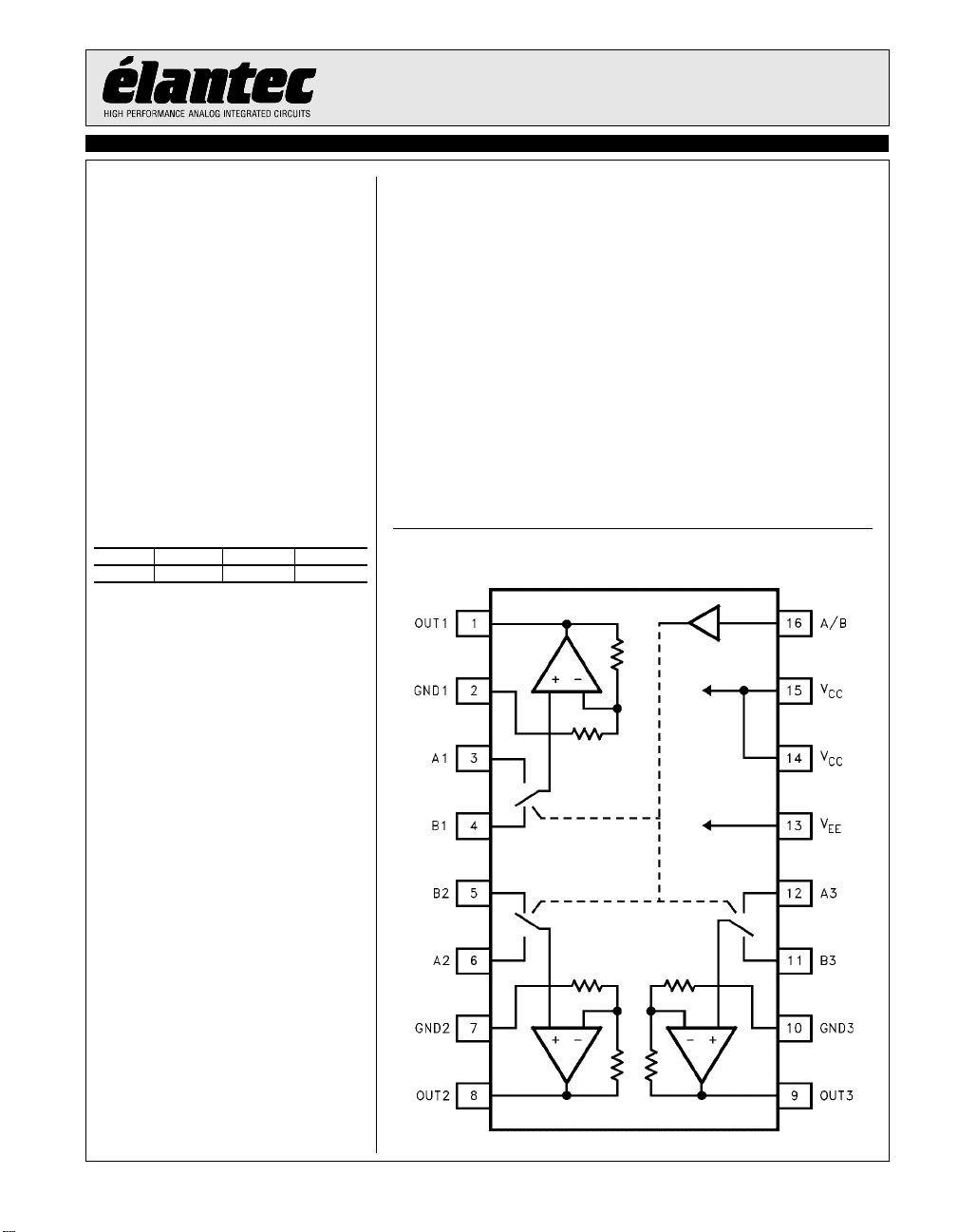
Connection Diagrams
© 1995 Elantec, Inc.
November 12, 1999
Page 2
EL4332C
Triple 2:1 300 MHz Mux-Amp AV =2
EL4332C
Absolute Maximum Ratings (T
VCC to V
EE
to any GND 12V
V
CC
to any GND 12V
V
EE
Continuous Output Current 45 mA
Any Input V
= 25 °C)
A
- 0.3V to VCC + 0.3V
EE
Input Current, Any Input 5 mA
14V
Power Dissipation See Curves
Operating Temperature -40°C to 85°C
Junction Temperature 170°C
Storage Temperature -60°C to +150°C
Important Note:
All parameters having Min/Max specifications are guaranteed. The Test Level column indicates the specific device testing actually performed during
production and Quality inspection. Elantec performs most electrical tests using modern high-speed automatic test equipment, specifically the LTX77
Series system. Unless otherwise noted, all tests are pulsed tests, therefor T
= TC = TA.
J
Test Level Test Procedure
I 100% production tested and QA sample tested per QA test plan QCX0002.
II 100% production tested at T
= 25°C and QA sample tested at TA = 25°C, T
A
MAX
and T
per QA test plan QCX0002.
MIN
III QA sample tested per QA test plan QCX0002.
IV Parameter is guaranteed (but not tested) by Design and Characterization Data.
V Parameter is typical value at T
= 25°C for information purposes only.
A
DC Electrical Characteristics
VCC = +5V, VEE = -5V, Temperature = 25°C, RL = ×
Parameter Description Min Typ Max
V
OS
dV
OS
R
IN
I
B
dI
B
A
V
dA
V
C
IN
Input Referred Offset Voltage 8 20 II mV
Input Referred Offset Voltage Delta
[1]
28II mV
Input Resistance 30 VkΩ
Input Bias Current -7 -30 II µA
Input Bias Current Delta
[1]
0.5 4.0 II µA
Gain 1.94 2.00 2.06 II V/V
[1]
Gain Delta
0.5 2.5 II %
Input Capacitance 3.3 VpF
PSRR Power Supply Rejection Ratio 50 70
V
O
Output Voltage Swing into 500Ω load ±2.7 ±3.6 II V
Output Voltage Swing into 150Ω load +3/-2.7
I
OUT
Xtalk
Xtalk
V
IH
V
IL
I
IL
I
IH
I
S
Current Output, Measured with 75W Load
Crosstalk from Non-selected Input (at DC) -70 -100 III dB
AB
Crosstalk from one Amplifier to another Amplifier -70 -100 VdB
CH-CH
Input Logic High Level 2.0 II V
Input Logic Low Level 0.8 II V
Logic Low Input Current (VIN = 0V) -0.3 -40 -80 II µA
Logic High Input Current (VIN = 0V) -3 0 3 II µA
Total Supply Current 38 48 60 II mA
[2]
30 40 II mA
1. Each channel’s A- input to its B-input.
2. There is no short circuit prot ection on any output.
Test Level Units
II dB
VV
2
Page 3
EL4332C
Triple 2:1 300 MHz Mux-Amp AV =2
AC Electrical Characteristics
VCC = +5V, VEE = -5V, Temperature = 25°C, RL = 150Ω, CL = 3 pF.
Parameter Description Min Typ Max
BW -3 dB Bandwidth 300
BW 0.1dB ±0.1 dB Bandwidth 105
DG Differential Gain at 3.58 MHz 0.04
DP Differential Phase at 3.58 MHz 0.08
Pkg Peaking with Nominal Load 0.2
SR Slew Rate (4V Square Wave, Measured 25%–75%) 650
t
s
T
SW
OS Overshoot, V
ab 10M Input to Input Isolation at 10 MHz 60 VdB
I
SO
I
ch-ch 10M Channel to Channel Isolation at 10 MHz 61 VdB
SO
Settling Time to 0.1% of Final Value 13 Vns
Time to Switch Inputs 3 Vns
= 4 V
OUT
P-P
100M Input to Input Isolation at 100 MHz 40
100M Channel to Channel Isolation at 100 MHz 50
8 V%
Test Level Units
VMHz
VMHz
V%
V °
VdB
VV/µs
VdB
VdB
EL4332C
Pin Descriptions
Pin Name Function
A1, A2, A3 “A” inputs to amplifiers 1, 2 and 3 respectively
B1, B2, B3 “B” inputs to amplifiers 1, 2 and 3 respectively
GND1, GND2, GND3 These are the individual ground pins for each channel.
Out1, Out2, Out3 Amplifier outputs. Note: there is no short circuit protection on any output.
V
CC
V
EE
A/B Common input select pin, a logic high selects the “A” inputs, logic low selects the “B” inputs. CMOS/TTL compatible.
Positive power supply. Typically +5V.
Negative power supply. Typically -5V.
3
Page 4
EL4332C
Triple 2:1 300 MHz Mux-Amp AV =2
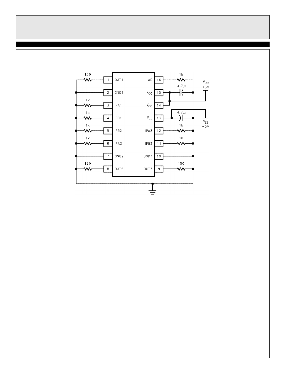
EL4332C
Burn In Schematic
4
Page 5
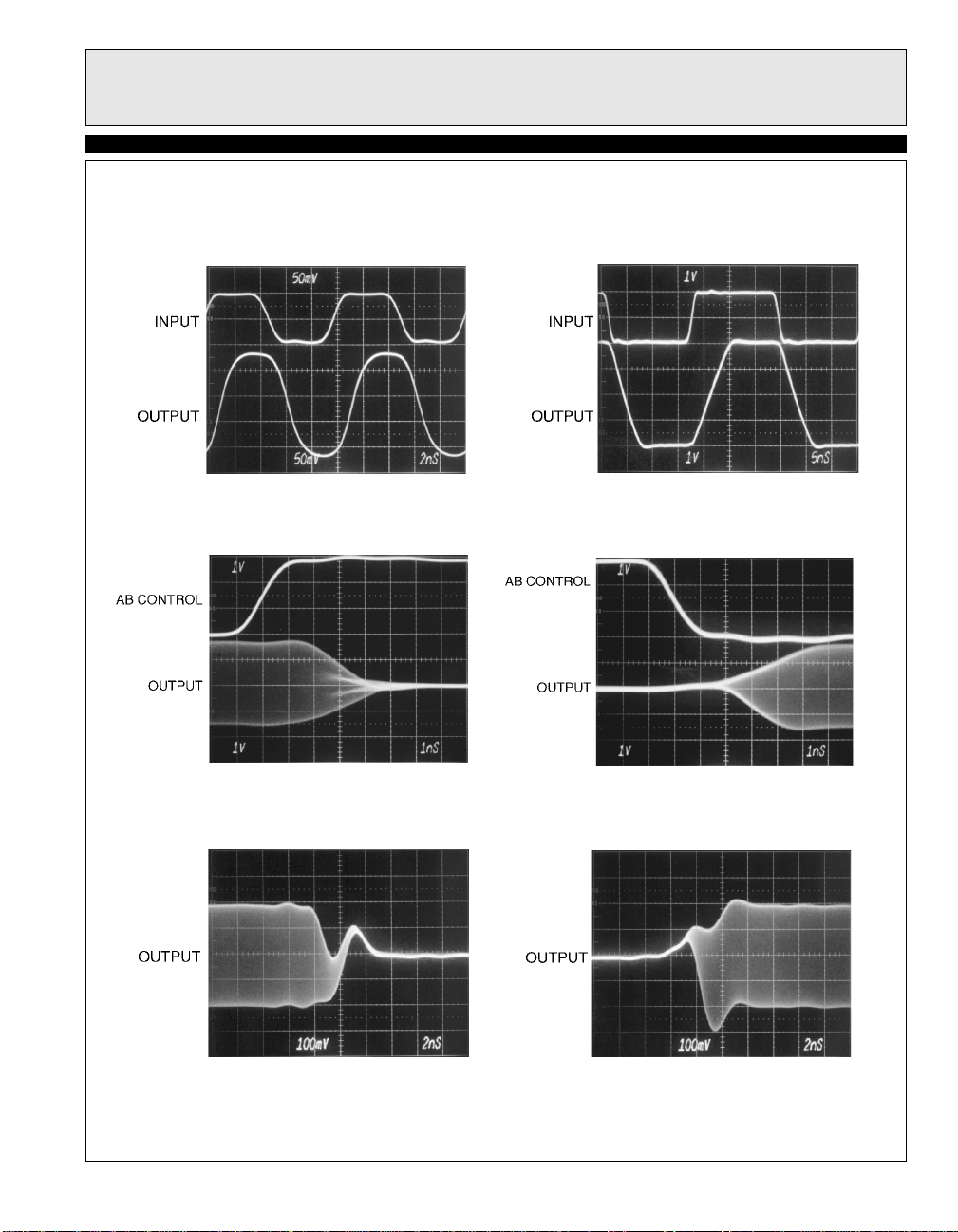
Typical Performance Curves
Small Signal Transient Response Large Signal Transient Response
EL4332C
EL4332C
Triple 2:1 300 MHz Mux-Amp AV =2
Switching to Ground from a Large
Signal Uncorrelated Sine Wave
Switching to Ground from a Small
Signal Uncorrelated Sine Wave
Switching from Ground to a Large
Signal Uncorrelated Sine Wave
Switching from Ground to a Small
Signal Uncorrelated Sine Wave
5
Page 6
EL4332C
Triple 2:1 300 MHz Mux-Amp AV =2
EL4332C
Switching Glitch
(Inputs at Ground)
Switching from Ground to a
Family of DC Levels
Switching from a Family of DC
Levels to Ground
Channel A/B Switching Delay
Gain vs Frequency Gain vs Frequency
6
Page 7

Triple 2:1 300 MHz Mux-Amp AV =2
-3 dB BW vs Supply Voltage Bandwidth vs Die Temperature
EL4332C
EL4332C
Frequency Response with Capacitive
Loads
A-Input to B–Input Isolation Channel-Channel Isolation
Input Voltage Noise over Frequency
7
Page 8

EL4332C
Triple 2:1 300 MHz Mux-Amp AV =2
EL4332C
Output Swing vs Supply Voltage
Supply Current vs Supply Voltage
Slew Rate vs Supply Voltage
Slew Rate vs Die Temperature
A-Input to B–Input Isolation
Maximum Power Dissipation
8
Page 9

EL4332C
Triple 2:1 300 MHz Mux-Amp AV =2
EL4332C
Applications
Figure 1 shows a typical use for the EL4332C. The circuit is a component video (R,G,B or Y,U,V)
multiplexer. Since the gain of the internal amplifiers has
been set to 2, the o nly ext ra compon ents n eeded are th e
supply decoupling capacitors and the back terminati ng
resistors, if transmission lines are to be driven. The
EL4332 can drive backmatched 50Ω or 75Ω loads.
Figure 1. Typical Connection for a 2:1 Component Video Multiplexer
9
Page 10

EL4332C
Triple 2:1 300 MHz Mux-Amp AV =2
EL4332C
Grounds
It will be noticed that each mux-amp channel has its own
separate ground pin. These ground pins have been kept
separate to keep the channel separation inside the chip as
large as possible. The feedback resistors use these
ground pins as their reference. The resistors total 400Ω,
so there is a significant signal current flowing from these
pins to ground.
The ground pins should all be connected togeth er, to a
ground plane underneath the chip. 1 oz. copper for the
ground plane is highly recommended.
Further notes and recommended practices for high speed
printed cir cuit b oard la yout c an b e f oun d i n th e t u tor ial s
in the Elantec databooks.
Supplies
Supply bypass ing sho uld be as phys ically near th e power
pins as possible. Chip capacitors should be used to minimize lead inductance. Note that larger values of
capacitor tend to have larger internal inductances. So
when designing for 3 transmission lines or similar moderate loads, a 0.1 µF ceramic capacitor right next to the
power pin in parallel with a 22 µF tantalum capacitor
placed as close to the 0.1 µF is recommended. For lighter
loadings, or if not all the channels are being used, a single 4.7 µF capacitor has been found quite adequate.
Note that component video signals do tend to have a
high level of signal correlation. This is especially true if
the video sig nal ha s b een d er ive d from 3 sy nchr on ous ly
clocked DACs. Thi s correspond s to all three chan nels
drawing large slew currents simultaneous ly from the
supplies. Thus, pr oper bypassing is critical.
current, typically < 30 µA, for a logic “low”. If left to
float, it will be a logic “high”.
Figure 2. Simplified Logic Input Stage
The input PNP transistors have sufficient gain that a
simple level shift circuit (see Figure 3) can be used to
provide a simple interface with Emitter Coupled Logic.
Typically, 200 mV is enough to switch from a solid
logic “low” to a “high.”
Logic Inputs
The A/B select, logic input, is internally referenced to
ground. It is set at 2 diode drops above ground, to give a
threshold of about 1.4V (see Figure 2). The PNP input
transistor requires that the driving gate be able to sink
Figure 3. Adapting the Select Pin
for ECL Logic Levels
The capacitor Cff is only in the network to prevent the
A/B pin’s capacitance from slowing the control signal.
The network shown level shifts the ECL le vels, -0.7V to
-1.5V to +1.6V and +1.1V respectiv el y. T he te rm inatin g
resistor, Rtt, is required since the open emitter of the
ECL gate can no t si nk curre nt. If a -2 V rail is n ot bei ng
10
Page 11

EL4332C
Triple 2:1 300 MHz Mux-Amp AV =2
EL4332C
used, a 220Ω to 330Ω resistor to the -5.2V rail would
have the same effect.
Expanding the Multiplexer
In Figure 4, a 3:1 multiplexer circuit is shown. T he
expansion to mo re in pu ts is ve ry st rai ght for ward . Sinc e
the EL4332C has a fixed gain of 2, interstag e attenua tors
may be required as shown in Figure 3. The truth table for
the 3:1 multiplexer select lines is:
XY Mux Output
0 0 R3, G3, B3 0 1 R2, G2, B2 1 X R1, G1, B1
When interstage attenuators are used, the values should
be kept down in the region of 50Ω–300Ω. This is to prevent a combination of circuit board stray capacitance
and the EL4332C’s input capacitance form ing a signifi-
cant pole. For example, if instead of 100Ω as shown,
resistor s of 1 kΩ had been used, and assuming 3 pF of
stray and 3 pF of input capacitance, a pole wou ld be
formed at about 53 MHz.
Figure 4. Typical Connection for a 3:1 Component Video Multiplexer
11
Page 12

EL4332C
Triple 2:1 300 MHz Mux-Amp AV =2
EL4332C
A Bandwidth Selectable Circuit
In Figure 5, a circuit is shown that allows three signals
to be either low pass filtered or full bandwidth.
This could be useful where an inp ut signal is frequent ly
noisy. The component val ues shown
give a Butterworth LPF respon se, with a -3 dB frequency of 50 MHz. Note agai n, the resistor values are
low, so that stray capacitance does not affect the desired
cut-off frequency.
Figure 5. Switched 50 MHz Low Pass Filter for High/Low Resolution Monitors
12
Page 13

Triple 2:1 300 MHz Mux-Amp AV =2
EL4332 Macromodel
* EL4332 Macromodel
* Revision A, April 1996
****************************************************************************
*Applications Hints. The EL4332 has two V
*pins. The V
*but the ground pins (GND1, GND2, and GND3 (nodes 2, 7, and 10, respectively)
*must be connected to ground (node 0) using a le-6W resistor. Alternatively,
* nodes 2, 7, and 10 may be connected to ground through a 25
* with a 4 nH inductor to simulate package and PCB parasitics.
****************************************************************************
* Connections:
* OUT1
* | GND1
* | | A1
* | | | B1
* | | | | B2
* | | | | | A2
* | | | | | | GND2
* | | | | | | | OUT2
* | | | | | | | |
* | | | | | | | |
* 1 2 3 4 5 6 7 8
*
* OUT3
* | GND3
* | | B3
* | | | A3
* | | | | V
* | | | | | V
* | | | | | | V
* | | | | | | | A/B
* | | | | | | | |
* | | | | | | | |
* 9 10 11 12 13 14 15 16
************A B Switch ***************
Rshort 14 15 le-12
rshort1 15 0 100 Meg
Isw 14 110 1.5 mA
vref 111 0 1.6V
q1 101 16 110 qp
q2 102 111 110 qp
R1 101 13 500
R2 102 13 500
Rd1 107 0 100
Esw 107 0 table {v(102, 101)*100} (0,0) (1,1)
*
************Amplifier #1 *************
q131 103 3 112 qp
q141 104 114 113 qp
q151 105 4 115 qp
q161 106 117 116 qp
Ia11 14 112 1 mA
Ia21 14 113 1 mA
Ib11 14 115 1 mA
Ib21 14 116 1 mA
Rga1 112 113 275
Rgb1 115 116 275
R31 103 13 275
R41 104 13 275
R51 105 13 275
R61 106 13 275
R71 1 114 400
pins (pins 14 and 15 are internally shorted together in the model,
CC
EE
CC
pins, one VEE pin, and three ground
CC
Ω resistor in parallel
CC
EL4332C
EL4332C
13
Page 14

EL4332C
Triple 2:1 300 MHz Mux-Amp AV =2
EL4332C
R81 114 2 400
R911 117 400
R110 117 2 400
Ediff1 108 0 value {(v(104,103)*v(107))+(v(106,105)*(1-v(107)))}
rdiff1 108 0 1K
*
*Compensation Section
*
ga1 0 134 108 0 1m
rh1 134 0 5 Meg
cc1 134 0 0.6 pF
*
*Poles
*
ep1 141 0 134 0 1.0
rpa1 141 142 200
cpa1 142 0 0.75 pF
rpb1 142 143 200
cpb1 143 0 0.75 pF
*
*Output Stage
*
i011 15 150 1.0 mA
i021 151 13 1.0 mA
q71 13 143 150 qp
q81 15 143 151 qn
q91 15 150 152 qn
q101 13 151 153 qp
ros11 152 1 2
ros21 153 1 2
*
************Amplifier #2***********
q231 203 6 212 qp
q241 204 214 213 qp
q251 205 5 215 qp
q261 206 217 216 qp
Ia12 14 212 1 mA
Ia22 14 213 1 mA
Ib12 14 215 1 mA
Ib22 14 216 1 mA
Rga2 212 213 275
Rgb2 215 216 275
R231 203 13 275
R241 204 13 275
R251 205 13 275
R261 206 13 275
R271 8 214 400
R281 214 7 400
R291 8 217 400
R210 217 7 400
Ediff2 208 0 value {(v(204,203)*v(107))+(v(206,205)*(1-v(107)))}
rdiff2 208 0 1K
*
* Compensation Section
*
ga2 0 234 208 0 1m
rh2 234 0 5 Meg
cc2 234 0 0.6 pF
*
* Poles
*
ep2 241 0 234 0 1.0
rpa2 241 242 200
cpa2 242 0 0.75 pF
14
Page 15

Triple 2:1 300 MHz Mux-Amp AV =2
rpb2 242 243 200
cpb2 243 0 0.75 pF
*
*Output Stage
*
i0 12 15 250 1.0 mA
i022 251 13 1.0 mA
q271 13 243 250 qp
q281 15 243 251 qn
q291 15 250 252 qn
q201 13 251 253 qp
ros12 252 8 2
ros22 253 8 2
*
************Amplifier #3 ************
q331 303 12 312 qp
q341 304 314 313 qp
q351 305 11 315 qp
q361 306 317 316 qp
Ia13 14 312 1 mA
Ia23 14 313 1 mA
Ib13 14 315 1 mA
Ib23 14 316 1 mA
Rga3 312 313 275
Rgb3 315 316 275
R331 303 13 275
R341 304 13 275
R351 305 13 275
R361 306 13 275
R371 9 314 400
R381 314 10 400
R391 9 317 400
R310 317 10 400
Ediff3 308 0 value {( v(304,303)*(v(107))+(v(306,305)*(1-v(107)))}
rdiff3 308 0 1K
*
* Compensation
*
ga3 0 334 308 01m
rh3 334 0 5 Meg
cc3 334 0 0.6 pF
*
* Poles
*
ep3 341 0 3340 1.0
rpa3 341 342 200
cpa3 342 0 0.75 pF
rpb3 342 343 200
cpb3 343 0 0.75 pF
*
* Output Stage
*
i013 15 350 1.0 mA
i023 351 13 1.0 mA
q371 13 343 350 qp
q381 15 343 351 qn
q391 15 350 352 qn
q301 13 351 353 qp
ros13 352 9 2
ros23 353 9 2
*
* Power Supply Current
*
ips 15 13 22 mA
EL4332C
EL4332C
15
Page 16

EL4332C
Triple 2:1 300 MHz Mux-Amp AV =2
EL4332C
*
*Models
*
.model qp pnp(is=1.5e-16 bf=300 tf=0.01 ns)
.model qn npn(is=0.8e-18 bf=300 tf=0.01 ns)
.ends
16
Page 17

EL4332C
Triple 2:1 300 MHz Mux-Amp AV =2
EL4332C
General Disclaimer
Specifications contained in this data sheet are in effect as of the publicat ion date shown. Elantec, Inc. re serves the r ight to make changes in th e circuitry or specifications cont ained herein at a ny time without notice. Elante c, Inc. assumes no res ponsibili ty for t he us e of any circuits described
herein and makes no representations that they are free from patent infringement.
WARNING - Life Support Policy
Elantec, Inc. products are not authorized for and should not be used
within Life Support Systems without the specific written consent of
Elantec, Inc. Life Support systems are equipment intend ed to sup-
Elantec, Inc.
1996 Tarob Court
Milpitas, CA 95035
Telephone: (408) 945-1323
(800) 333-6314
Fax: (408) 945-9305
European Office: 44-71-482-4596
port or sustain life and whose failure to perform when properly used
in accordance with instructions provided can be reasonably
expected to result in significant personal injury or death. Users contemplating applicatio n of Elantec, In c. Products in Li fe Support
Systems are requested to contact Elantec, Inc. factory headquarters
to establish suitable terms & conditions for these applications. Elantec, Inc. ’s warranty is limited to replacement of defective
components and does not cov er injury to per sons or prop erty or
other consequential damages.
November 12, 1999
17
Printed in U.S.A.
 Loading...