

Page 1
EL4101C - Preliminary
500MHz Video Front End - 4:1MUX + DC-Restore
EL4101C - Preliminary
Features
• 4:1 multiplexer with monitor out
• DC-restore amplifier
• ±5V operation
• 500MHz bandwidth
Applications
• HDTV/DTV analog inputs
• Video projectors
• Computer monitors
• Set top boxes
• Security video
• Broadcast video equipment
Ordering Information
Part No. Package Tape & Reel Outline #
EL4101CU 24-Pin QSOP MDP0040
General Description
The EL4101C VFE (Video Front End) is designed to perform the basic
input processing functions in an analog video system as well as provide
analog input processing for digital video systems. The EL4101C VFE
contains a 4:1 MUX input and a DC-restore amplifier. The MUX input
can be used to select which input to use. The DC-restore allows the
input signal to be positioned to the correct voltage level for either analog or digital processing. A buffered output of the MUX selection is
also available for use as a monitor output.
With a 500MHz bandwidth and only 40mA supply current, the
EL4101C is ideal for use in portable and fixed projectors, as well as
HDTV, DTV and other high performance video applications.
The EL4101C is available in the 24-pin QSOP package and is specified
for operation over the full -40°C to +85°C temperature range.
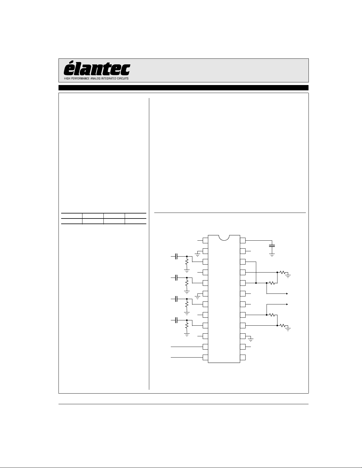
Connection Diagram
SIG0
SIG1
SIG2
SIG3
HPULSE
+5V
1
HOLD
2
GNDL2
3
IN0
4
VS1+
5
IN1
6
GNDI
7
IN2
8
-5V
VS1-
9
IN3
CAP
DCREF
DCFDBK
VFDBK
VOUT
VS2+
VS2-
MOUT
MFDBK
24
23
DCV
22
21
20
19
+5V
18
-5V
17
16
0.33µF
R
GV
R
FV
Video Out
RLV=150Ω
Monitor Out
R
RLM=150Ω
FM
R
GM
10
N.C.
11
LOGICD0
LOGICD1
Note: Pin #6 should be a good high frequency ground
Note: All information contained in this data sheet has been carefully checked and is believed to be accurate as of the date of publication; however, this data sheet cannot be a “controlled document”. Current revisions, if any, to these
specifications are maintained at the factory and are available upon your request. We recommend checking the revision level before finalization of your design documentation.
© 2001 Elantec Semiconductor, Inc.
D0
12
D1
GNDL
PDWN
N.C.
15
14
LOGICPD
13
August 9, 2001
Page 2
EL4101C - Preliminary
500MHz Video Front End - 4:1MUX + DC-Restore
Absolute Maximum Ratings (T
Values beyond absolute maximum ratings can cause the device to be prematurely damaged. Absolute maximum ratings are stress ratings only
and functional device operation is not implied.
Supply Voltage (VS+ to VS-) 11V
EL4101C - Preliminary
Input Voltage VS- - 0.3V, VS+ +0.3V
= 25°C)
A
Storage Temperature Range -65°C to +150°C
Ambient operating Temperature -40°C to +85°C
Operating Junction Temperature 125°C
Power Dissipation See Curves
Important Note:
All parameters having Min/Max specifications are guaranteed. Typ values are for information purposes only. Unless otherwise noted, all tests are at the
specified temperature and are pulsed tests, therefore: TJ = TC = TA.
Electrical Characteristics
VS1+ = VS2+ = 5V, VS1- = VS2- = -5V, R
Parameter Parameter Description Conditions Min Typ Max Unit
Supply
IS1+ Positive Supply Current 1 25 mA
IS- Negative Supply Current 38 mA
IS2+ Positive Supply Current 2 VIN = 0, IL = 0 15 mA
I
+ Positive Supply Current 1 in Standby Standby 3.8 mA
S1S
ISS- Negative Supply Current in Standby Standby 2 mA
I
+ Positive Supply Current 2 in Standby Standby 236 µA
S2S
Input
I
B
I
BO
V
IH
V
IL
I
IL
I
IH
t
SH
Input Bias Current VIN = 0V -22.4 -2.2 6.1 µA
Input Bias Current Drift with Temp. VIN = 0V TBD nA/°C
Input High Voltage 2 V
Input Low Voltage 0.8 V
Low Input Current for D0, D1, PDWN, HOLD VIN = 0V 25 48 75 µA
High Input Current for D0, D1, PDWN, HOLD VIN =5V 0 - 10 µA
Sample and Hold Delay Time 12 ns
Output
V
OSM
V
OS
δV
OS
V
OH
V
OL
I
SC
Output Offset Voltage - Monitor VIN = 0V -400 18 420 mV
DC-restore Offset Voltage Auto-zero on, DC
Output Offset Voltage Drift - Video Auto-zero on TBD µV/°C
Output Voltage Swing, Pos. AV = +1, monitor & video outputs 3.44 3.5 V
Output Voltage Swing, Neg. AV = +1, monitor & video outputs -3.43 -3.5 V
Output Short Circuit Current RL = 10Ω, source or sink 65 100 140 mA
AC Performance
SR Slew Rate - Video Out (20%-80%) V
SRM Slew Rate - Monitor Out (20%-80%) V
OS Output Overshoot, Video V
OSM Output Overshoot, Monitor V
t
t
V
t
V
V
I
I
S
SM
REF
SD
OHS
OSB
CCL
DC
Settling Time to 1%, Video Hold mode 10 ns
Settling Time to 1%, Monitor 10 ns
DC-restore -Reference Voltage Range VIN = -2V to +2V -2 - 2 V
DC-restore - Settling Time to 1% Sample mode on 2.5 µs
DC-restore - Video Output Hold Step S - H transition -0.5 mV
DC-restore - Offset vs. Black Level Sample mode on -1 -0.6 1 mV/V
DC-restore - Charge Current Limit, I
DC-restore - Droop Current, I
= RGV = RFM = RGM =375, R
FV
CAP
CAP
= RLM = 150Ω, CLV = CLM = 3p, CH = 0.33n, GAIN = 2.
LV
= 0 -5 - 5 mV
REF
OUT
OUT
OUT
OUT
= 4V
= 4V
= 1V
= 1V
P-P
P-P
P-P
P-P
1000 2100 4500 V/µs
1250 2100 3900 V/µs
TBD %
TBD %
Sample mode on 210 260 345 µA
Hold mode on -30 - 30 nA
2
Page 3

EL4101C - Preliminary
500MHz Video Front End - 4:1MUX + DC-Restore
Electrical Characteristics
VS1+ = VS2+ = 5V, VS1- = VS2- = -5V, R
Parameter Parameter Description Conditions Min Typ Max Unit
BW 3dB Bandwidth, Video Out 500 MHz
BWM 3dB Bandwidth, Monitor Out 1000 MHz
0.1BW ±0.1dB Flat Bandwidth, Video Out 25 MHz
0.1BWM ±0.1dB Flat Bandwidth, Monitor Out 18 MHz
Vp Peaking, Video 2.4 dB
Vpm Peaking, Monitor 4.5 dB
dP Diff. Phase @3.58MHz, Video TBD °
dG Diff. Gain @3.58MHz, Video TBD %
dPM Diff. Phase @3.58MHz, Monitor TBD °
dPG Diff. Gain @3.58MHz, Monitor TBD %
e
n
e
nm
1. Total unwanted output normalized by wanted (or expected) output; add -10dB to get channel-to-channel isolation
Noise Voltage at Input for VOUT TBD nV/√Hz
Noise Voltage at Input for MOUT TBD nV/√Hz
[1]
Crosstalk
Crosstalk
@10MHz 3 channel hostile -45 dB
[1]
@100MHz 3 channel hostile -20 dB
= RGV = RFM = RGM =375, R
FV
= RLM = 150Ω, CLV = CLM = 3p, CH = 0.33n, GAIN = 2.
LV
EL4101C - Preliminary
Parallel Programming Truth Table
Inputs
PDWN D1 D0
0 0 0 IN0 Selected
0 0 1 IN1 Selected
0 1 0 IN2 Selected
0 1 1 IN3 Selected
1 X X Standby - Powered Down
State
3
Page 4

EL4101C - Preliminary
500MHz Video Front End - 4:1MUX + DC-Restore
Pin Descriptions
Pin Number Pin Name Pin Type Pin Description
EL4101C - Preliminary
1 HOLD Logic Input Hold pulse for DC-restore function
2 GNDL2 Logic Ground Logic ground for “hold” buffer
3 IN0 High Frequency Signal Video input #0
4 VS1+ Power Positive power pin for quiet supply currents
5 IN1 High Frequency Signal Video input #1
6 GNDI Analog Signal Reference voltage for attenuation function
7 IN2 High Frequency Signal Video input #2
8 VS1- Power Negative power pin for quiet supply currents
9 IN3 High Frequency Signal Video input #3
10 No connection
11 D0 Logic Input Parallel control bit #0
12 D1 Logic Input Parallel control bit #1
13 No connection
14 PDWN Logic Input Power down input to put chip in low current standby mode
15 GNDL Logic Ground Logic ground for D0, D1, PWDN buffers
16 MFDBK High Frequency Signal Monitor amplifier feedback
17 MOUT High Frequency Signal Monitor amplifier output
18 VS2- Power Negative power pin for heavy, pulsatile supply currents
19 VS2+ Power Positive power pin for heavy, pulsatile supply currents
20 VOUT High Frequency Signal Video amplifier output
21 VFDBK High Frequency Signal Video amplifier feedback
22 DCFDBK Analog Signal Input to sample circuit
23 DCREF Analog Signal Reference DC voltage representing black level
24 CAP Analog Signal Sample storage capacitor for DC-restore circuit
4
Page 5

Block Diagram (Gain of 1)
EL4101C - Preliminary
EL4101C - Preliminary
500MHz Video Front End - 4:1MUX + DC-Restore
Input Video
Input Video
Input Video
Input Video
VS+
IN0
IN1
IN2
IN3
D0
D1
GNDL GND GNDL2 VS- P
M
FDBK
+
+
-
DWN
M
OUT
V
OUT
V
FDBK
DC
DC
HOLD
CAP
FDBK
REF
+
-
750Ω
C
750Ω
H
5
Page 6

EL4101C - Preliminary
500MHz Video Front End - 4:1MUX + DC-Restore
EL4101C - Preliminary
General Disclaimer
Specifications contained in this data sheet are in effect as of the publication date shown. Elantec, Inc. reserves the right to make changes in the circuitry or specifications contained herein at any time without notice. Elantec, Inc. assumes no responsibility for the use of any circuits described
herein and makes no representations that they are free from patent infringement.
WARNING - Life Support Policy
Elantec, Inc. products are not authorized for and should not be used
within Life Support Systems without the specific written consent of
Elantec, Inc. Life Support systems are equipment intended to sup-
Elantec Semiconductor, Inc.
675 Trade Zone Blvd.
Milpitas, CA 95035
Telephone: (408) 945-1323
(888) ELANTEC
Fax: (408) 945-9305
European Office: 44-118-977-6020
Japan Technical Center: 81-45-682-5820
port or sustain life and whose failure to perform when properly used
in accordance with instructions provided can be reasonably
expected to result in significant personal injury or death. Users contemplating application of Elantec, Inc. Products in Life Support
Systems are requested to contact Elantec, Inc. factory headquarters
to establish suitable terms & conditions for these applications. Elantec, Inc.’s warranty is limited to replacement of defective
components and does not cover injury to persons or property or
other consequential damages.
August 9, 2001
6
Printed in U.S.A.
 Loading...