

Page 1
EL4095C
Video Gain Control/Fader/Multiplexer
EL4095C August 1996 Rev D
Features
# Full function video fader
# 0.02%/0.02
phase
differential gain/
§
@
100% gain
# 25 ns multiplexer included
# Output amplifier included
# Calibrated linear gain control
g
#
5V tog15V operation
# 60 MHz bandwidth
# Low thermal errors
Applications
# Video faders/wipers
# Gain control
# Graphics overlay
# Video text insertion
# Level adjust
# Modulation
Ordering Information
Part No. Temp. Range Package Outline
EL4095CNb40§Ctoa85§C 14 Pin P-DIP MDP0031
EL4095CSb40
Ctoa85§C SO-14 MDP0027
§
General Description
The EL4095C is a versatile variable-gain building block. At its
core is a fader which can variably blend two inputs together and
an output amplifier that can drive heavy loads. Each input appears as the input of a current-feedback amplifier and with external resistors can separately provide any gain desired. The
output is defined as:
e
V
OUT
A*V
(0. 5VaV
INA
GAIN
)aB*V
INB
(0.5V–V
where A and B are the fed-back gains of each channel.
Additionally, two logic inputs are provided which each override
the analog V
control and force 100% gain for one input
GAIN
and 0% for the other. The logic inputs switch in only 25 ns and
provide high attenuation to the off channel, while generating
very small glitches.
Signal bandwidth is 60 MHz, and gain-control bandwidth
20 MHz. The gain control recovers from overdrive in only
70 ns.
The EL4095C operates from
g
5V tog15V power supplies, and
is available in both 14-pin DIP and narrow surface mount packages.
Ý
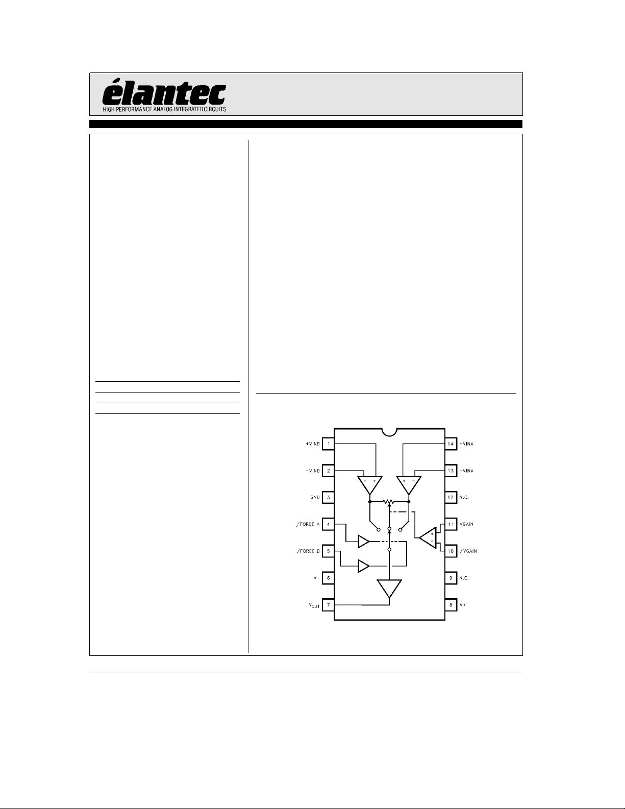
Connection Diagram
14-Pin DIP, SO
GAIN
),
Top View
Manufactured under U.S. Patent No. 5,321,371, 5,374,898
Note: All information contained in this data sheet has been carefully checked and is believed to be accurate as of the date of publication; however, this data sheet cannot be a ‘‘controlled document’’. Current revisions, if any, to these
specifications are maintained at the factory and are available upon your request. We recommend checking the revision level before finalization of your design documentation.
©
1992 Elantec, Inc.
4095– 1
Page 2
EL4095C
Video Gain Control/Fader/Multiplexer
Absolute Maximum Ratings
V
a
S
V
S
a
V
a
I
IN
V
GAIN
V
GAIN
Important Note:
All parameters having Min/Max specifications are guaranteed. The Test Level column indicates the specific device testing actually
performed during production and Quality inspection. Elantec performs most electrical tests using modern high-speed automatic test
equipment, specifically the LTX77 Series system. Unless otherwise noted, all tests are pulsed tests, therefore T
Test Level Test Procedure
Supply Voltage
Voltage between V
, Input Voltage (V
INA
V
INB
Current IntobV
Input Voltage V
INA
S
a
,bV
and V
INB
b
S
to (V
Input Voltage V
I 100% production tested and QA sample tested per QA test plan QCX0002.
II 100% production tested at T
III QA sample tested per QA test plan QCX0002.
IV Parameter is guaranteed (but not tested) by Design and Characterization Data.
V Parameter is typical value at T
T
MAX
and T
MIN
A
per QA test plan QCX0002.
e
(T
25§C)
A
a
18V
V
a
33V
b)b
0.3V
S
a
)a0.3V
S
5mA
g
5V
GAIN
b
to V
S
S
e
25§C and QA sample tested at T
e
25§C for information purposes only.
A
FORCE
I
OUT
T
A
T
J
T
ST
Internal Power Dissipation See Curves
a
Input Voltage
Output Current
Operating Temperature Range
b
1V toa6V
g
b
40§Ctoa85§C
35 mA
Operating Junction Temperature 0§Ctoa150§C
Storage Temperature Range
e
25§C,
A
b
65§Ctoa150§C
e
e
T
J
C
TA.
Open Loop DC Electrical Characteristics
e
g
V
S
Parameter Description
V
OS
I
a
B
I
b
B
CMRR Common Mode Rejection 65 80 I dB
b
CMRR
PSRR Power Supply Rejection Ratio 65 95 I dB
b
IPSR
R
OL
R
b
IN
V
IN
V
O
I
SC
V
IH
V
IL
I
FORCE
I
FORCE
e
15V, T
25§C, V
A
ground unless otherwise specified
GAIN
Input Offset Voltage 1.5 5 I mV
a
VINInput Bias Current 5 10 I mA
b
VINInput Bias Current 10 50 I mA
b
VINInput Bias Current
Common Mode Rejection
b
VINInput Current
Power Supply Rejection Ratio
Transimpedance 0.2 0.4 I MX
b
VINInput Resistance 80 V X
a
VINRange (Vb)a3.5 (Va)b3.5 I V
Output Voltage Swing (Vb)a2(V
Output Short-Circuit Current 80 125 160 I mA
Input High Threshold at
Force A or Force B Inputs
Input Low Threshold at
Force A or Force B Inputs
, High Input Current of Force A
or Force B, V
FORCE
, Low Input Current of Force A
or Force B, V
FORCE
Limits Test
Min Typ Max
Level
Units
0.5 1.5 I mA/V
0.2 2 I mA/V
a
b
)
2I V
2.0 I V
0.8 I V
b
e
5V
b
e
0V
440
50 I mA
b
650 I mA
TDis 0.7inTDis 4.0in
2
Page 3
EL4095C
Video Gain Control/Fader/Multiplexer
Open Loop DC Electrical Characteristics
e
g
V
S
Parameter Description
Feedthrough, Feedthrough of Deselected Input to Output,
Forced Deselected Input at 100% Gain Control
V
GAIN
V
GAIN
NL, Gain Gain Control Non-linearity,
RIN, VG Impedance between V
NL, A
A
A
I
S
e
15V, T
25§C, unless otherwise specified
A
, 100% Minimum Voltage at
V
for 100% Gain
GAIN
, 0% Maximum Voltage at
V
for 0% Gain
GAIN
e
g
V
e
1 Signal Non-linearity, V
V
e
0.5 Signal Non-linearity, V
V
e
0.25 Signal Non-linearity, V
V
0.5V
IN
Supply Current 17 21 I mA
GAIN
IN
IN
IN
and V
e
e
e
g
g
g
GAIN
1V, V
1V, V
1V, V
e
0.55V
GAIN
e
0V 0.03 V %
GAIN
eb
GAIN
0.25V 0.07 0.4 I %
Closed Loop AC Electrical Characteristics
e
g
V
S
noted
Parameter Description
SR Slew Rate; V
BW Bandwidth
dG Differential Gain; AC Amplitude of 286 mV
di Differential Phase; AC Amplitude of 286 mV
T
S
T
FORCE
BW, Gain
T
REC
15V, A
V
ea
e
1, R
F
Measured at
e
R
1kX,R
IN
fromb3V toa3V
OUT
b
2V anda2V
L
e
500X,C
at 3.58 MHz on DC Offset ofb0.7V, 0V anda0.7V
at 3.58 MHz on DC Offset ofb0.7V, 0V anda0.7V
Settling Time to 0.2%; V
Propagation Delay from V
Output Signal Enabled or Disabled Amplitude
b
3 dB Gain Control Bandwidth,
Amplitude 0.5 V
V
GAIN
fromb2V toa2V
OUT
e
FORCE
P-P
, Gain Gain Control Recovery from Overload;
fromb0.7V to 0V
V
GAIN
e
15 pF, C
L
A
V
A
V
A
V
A
V
A
V
A
V
A
V
A
V
IN
b
3 dB 60 MHz
b
1 dB 30 V MHz
b
0.1 dB 6 MHz
p-p
e
100% 0.02 V %
e
50% 0.07 %
e
25% 0.07 %
p-p
e
100% 0.02 V
e
50% 0.05
e
25% 0.15
e
100% 100 V ns
e
25% 100 ns
1.4V to 50%
Ð Contd.
Limits Test
Min Typ Max
60 75 I dB
0.45 0.5 0.55 I V
b
be
2 pF, T
Min Typ Max
0.55
b
0.5
b
0.45 I V
24 I%
4.5 5.5 6.5 I kX
k
0.01 V %
e
A
25§C, A
e
100% unless otherwise
V
Limits Test
330 V V/ms
25 V ns
20 V MHz
70 V ns
Level
Level
Units
TDis 2.4inTDis 3.8in
Units
§
§
§
3
Page 4
EL4095C
Video Gain Control/Fader/Multiplexer
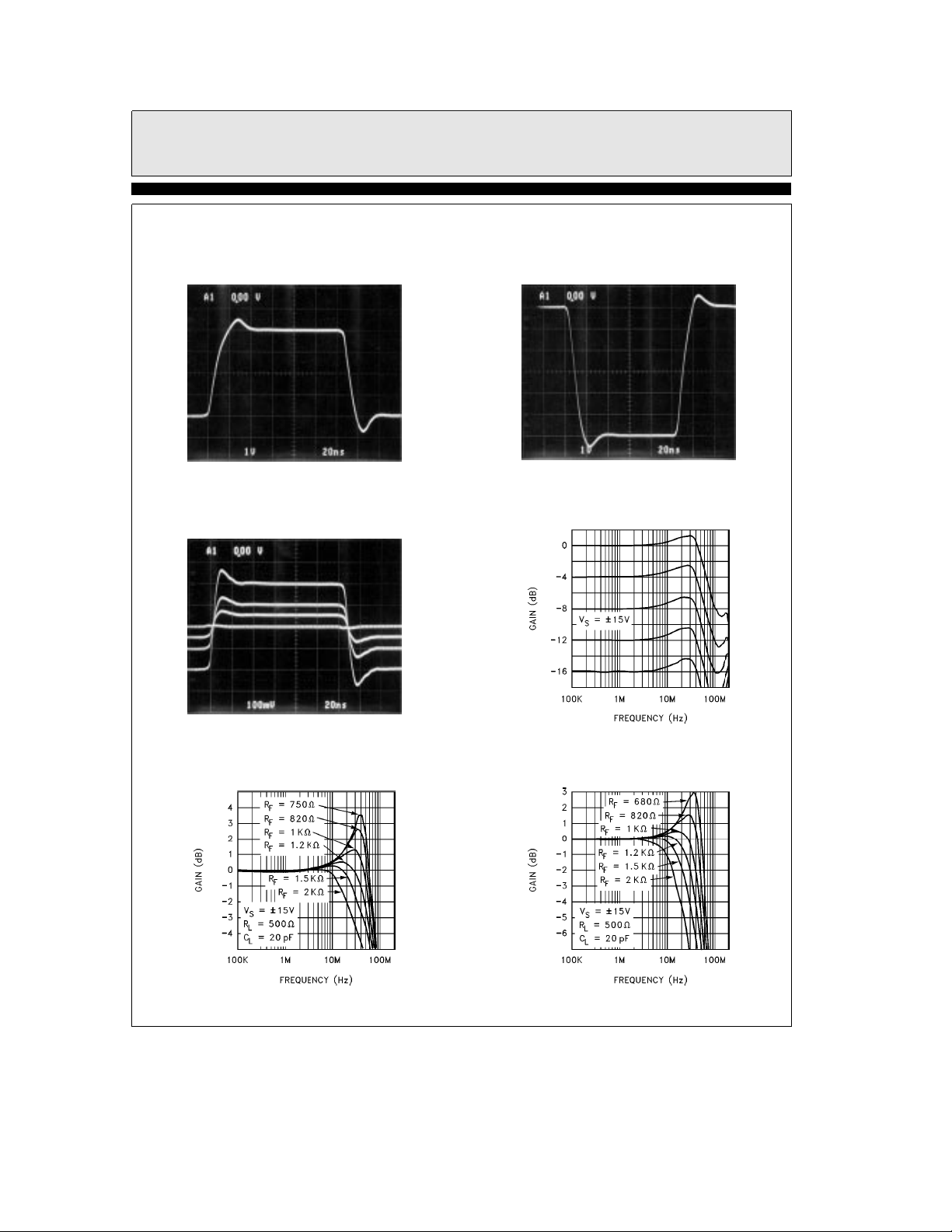
Typical Performance Curves
Large-Signal Pulse
Response Gain
ea
1
Small-Signal Pulse Response
for Various Gains
4095– 6
Large-Signal Pulse
V
ea
1
eb
1
Response Gain
Frequency Response for Different
Gains-A
4095– 7
Frequency Response with Different
Values of R
b
Gainea1
F
4095– 8
4095– 10
4095– 9
Frequency Response with Different
Values of R
b
Gaineb1
F
4095– 11
4
Page 5
EL4095C
Video Gain Control/Fader/Multiplexer
Typical Performance Curves
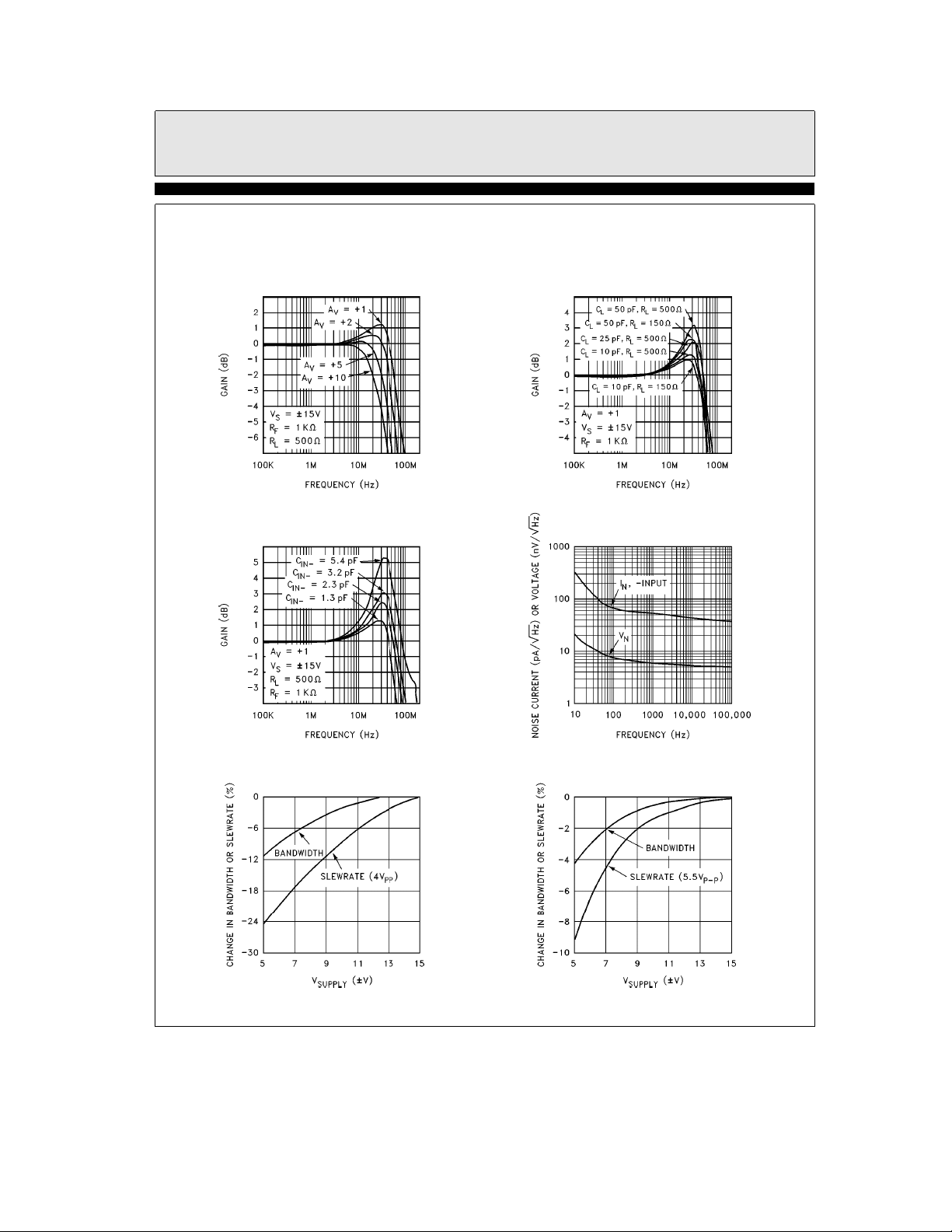
Frequency Response with Different Gains Load Capacitances and Resistances
Frequency Response with Various
Values of Parasitic C
b
IN
Ð Contd.
Frequency Response with Various
Input Noise Voltage and
Current vs Frequency
Change in Bandwidth and Slewrate with
Supply Voltage
b
Gainea1
Change in Bandwidth and Slewrate with
Supply VoltagebGaineb1
4095– 12
5
Page 6
EL4095C
Video Gain Control/Fader/Multiplexer
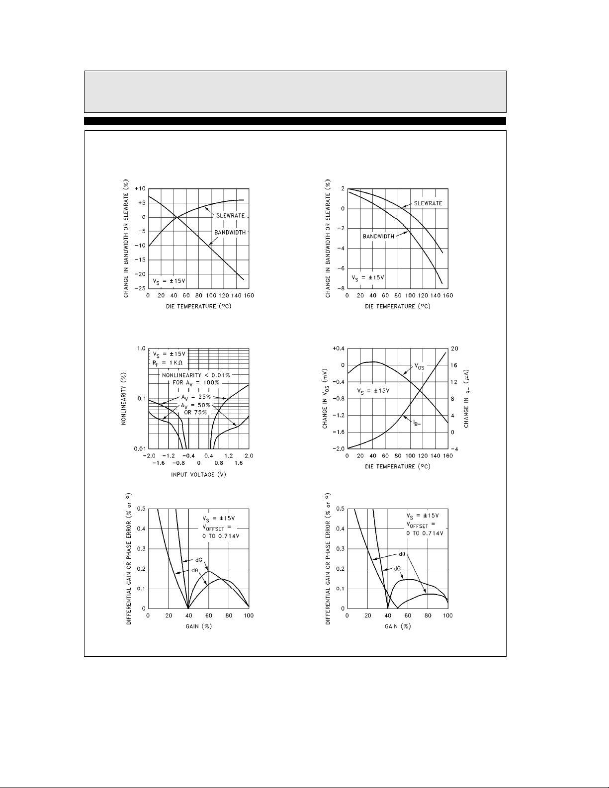
Typical Performance Curves
Change in Bandwidth and Slewrate
with TemperaturebGainea1
DC Nonlinearity vs Input Voltage
b
Gainea1
Ð Contd.
Change in Bandwidth and Slewrate
with TemperaturebGaineb1
Change in VOSand IB- vs die Temperature
Differential Gain and Phase Errors vs
Gain Control Setting
b
Gainea1
Differential Gain and Phase Errors vs
Gain Control SettingbGaineb1
4095– 13
6
Page 7
EL4095C
Video Gain Control/Fader/Multiplexer
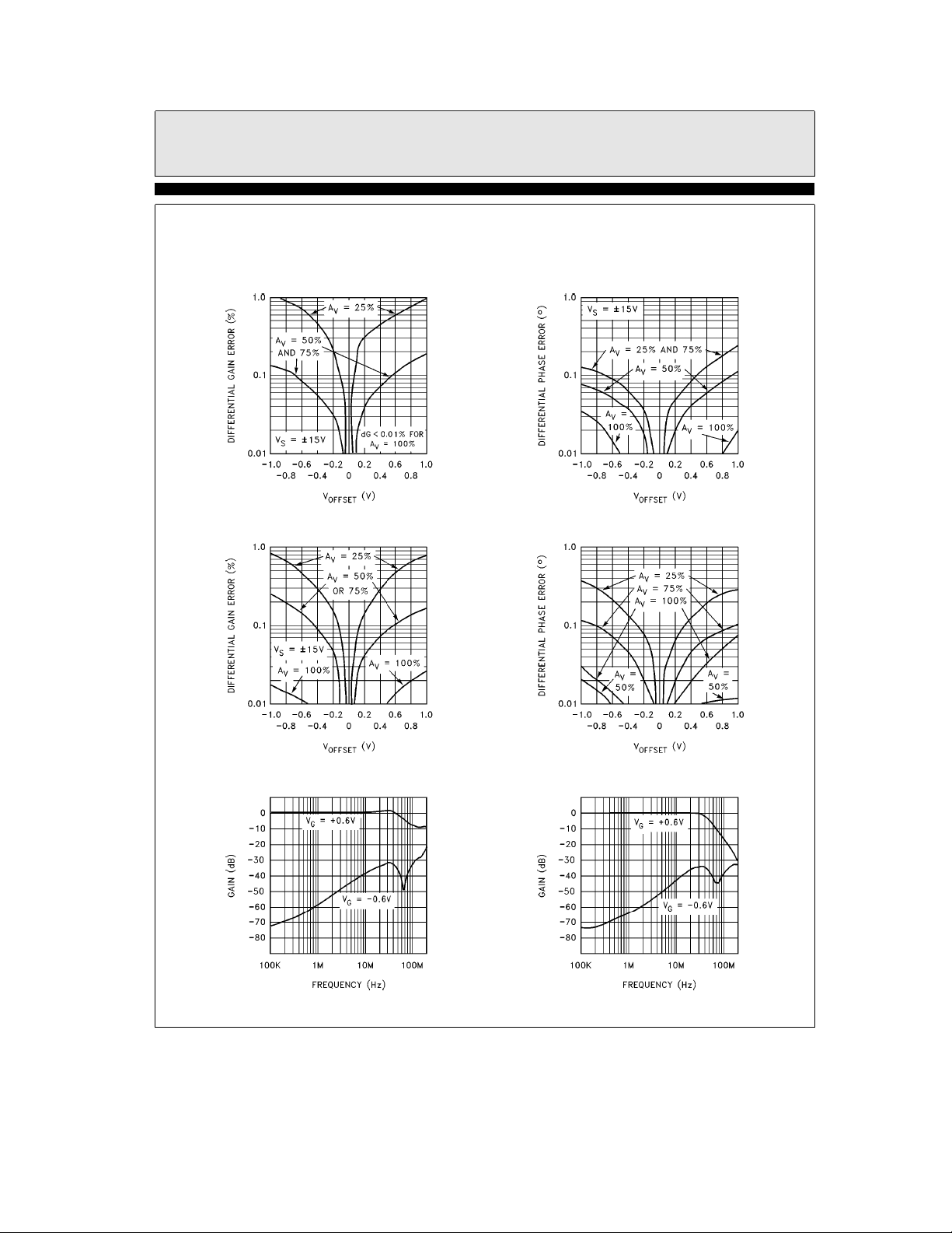
Typical Performance Curves
Differential Phase Error vs
DC OffsetbGainea1
Differential Phase Error vs
DC Offset
b
Gaineb1
Ð Contd.
Differential Phase Error vs
DC OffsetbGainea1
Differential Phase Error vs
DC OffsetbGaineb1
Attenuation over
Frequency
b
Gainea1
Attenuation over
FrequencybGaineb1
4095– 14
7
Page 8
EL4095C
Video Gain Control/Fader/Multiplexer
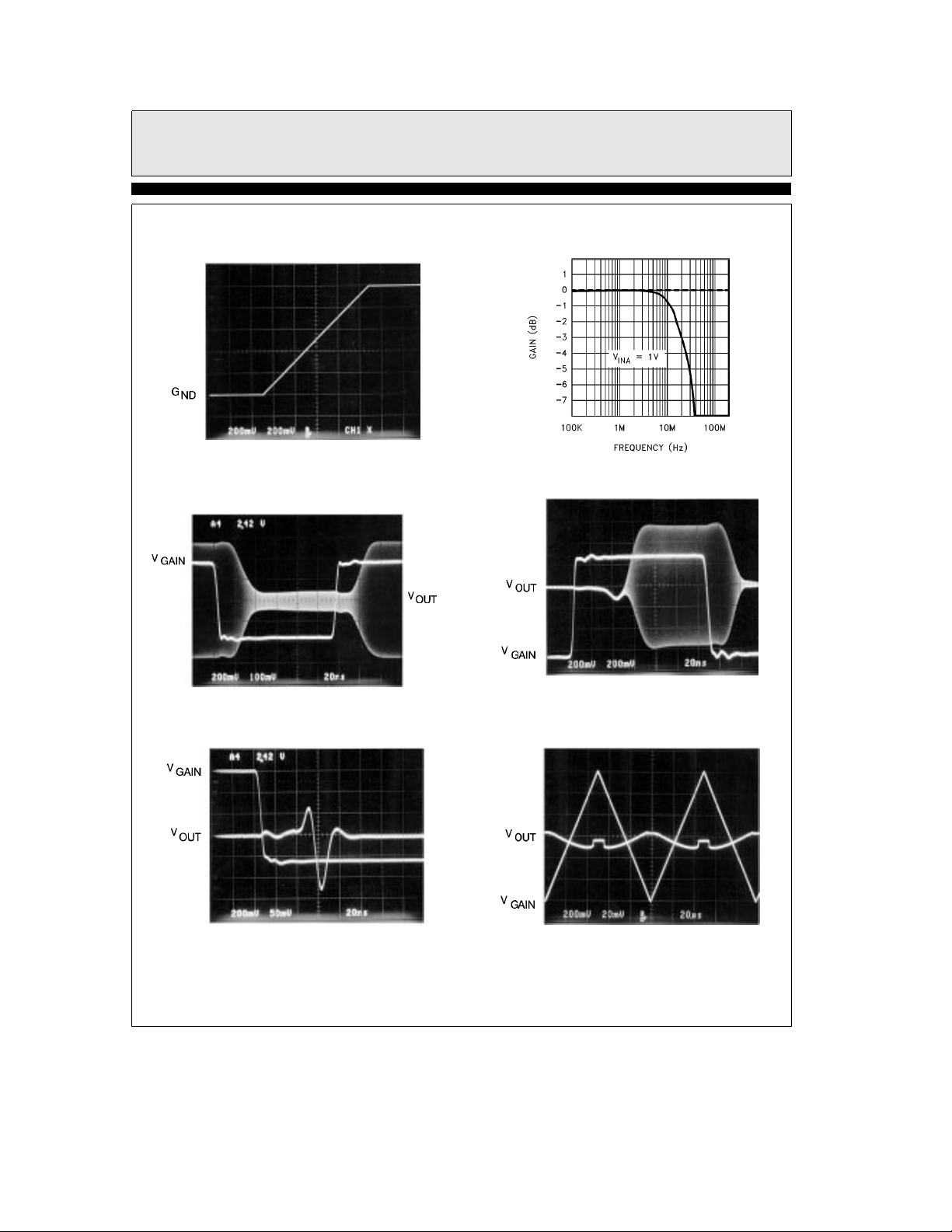
Typical Performance Curves
Gain vs VG(1 VDCat V
Gain Control Response to a Non-Overloading
Step, Constant Sinewave at V
INA
INA
)
Ð Contd.
4095– 15
Gain Control Gain vs Frequency
V
Overload Recovery Delay
GAIN
4095– 16
V
Overload Recovery
GAIN
ResponseÐNo AC Input
4095– 17
4095– 19
4095– 18
Cross-Fade Balanceb0V on
A
and BIN; Gain
IN
8
ea
1
4095– 20
Page 9

EL4095C
Video Gain Control/Fader/Multiplexer
Typical Performance Curves
Change in V
V
of Gain Control
0%
vs Supply Voltage
and
100%
Force Response
Ð Contd.
Change in V
V
of Gain Control
0%
vs V
GAIN
100%
Offset
and
Change in V
V
of Gain Control
0%
vs Die Temperature
100%
and
Force-Induced Output Transient
4095– 21
Supply Current vs Supply Voltage
4095– 22
4095– 24
4095– 23
Package Power Dissipation
vs Ambient Temperature
4095– 25
9
Page 10

EL4095C
Video Gain Control/Fader/Multiplexer
Test Circuit, A
V
ea
1
4095– 26
10
Page 11

EL4095C
Video Gain Control/Fader/Multiplexer
Applications Information
The EL4095 is a general-purpose two-channel
fader whose input channels each act as a currentfeedback amplifier (CFA) input. Each input can
have its own gain factor as established by external resistors. For instance, the Test Circuit shows
two channels each arranged as
traditional single feedback resistor R
from V
The EL4095 can be connected as an inverting
amplifier in the same manner as any CFA:
to thebVINof each channel.
OUT
a
1 gain, with the
connected
F
EL4095C In Inverting Connection
Frequency Response
Like other CFA’s, there is a recommended feedback resistor, which for this circuit is 1 KX. The
value of RF sets the closed-loop
width, and has only a small range of practical
variation. The user should consult the typical
performance curves to find the optional value of
R
for a given circuit gain. In general, the band-
F
width will decrease slightly as closed-loop gain is
increased; R
bandwidth loss. Too small a value of R
cause frequency response peaking and ringing
during transients. On the other hand, increasing
R
will reduce bandwidth but improve stability.
F
can be reduced to make up for
F
b
3 dB band-
will
F
4095– 27
11
Page 12

EL4095C
Video Gain Control/Fader/Multiplexer
Applications Information
Stray capacitance at each
b
VINterminal should
Ð Contd.
absolutely be minimized, especially in a positivegain mode, or peaking will occur. Similarly, the
load capacitance should be minimized. If more
than 25 pF of load capacitance must be driven, a
load resistor from 100X to 400X can be added in
parallel with the output to reduce peaking, but
some bandwidth degradation may occur. A
‘‘snubber’’ load can alternatively be used. This is
a resistor in series with a capacitor to ground,
150X and 100 pF being typical values. The advantage of a snubber is that it does not draw DC
load current. A small series resistor, low tens of
ohms, can also be used to isolate reactive loads.
Distortion
The signal voltage range of theaVINterminals
is within 3.5V of either supply rail.
One must also consider the range of error currents that will be handled by the
nals. Since the
b
VINof a CFA is the output of a
buffer which replicates the voltage at
ror currents will flow into the
b
VINtermi-
a
b
VIN, er-
VINterminal.
When an input channel has 100% gain assigned
to it, only a small error current flows into its negative input; when low gain is assigned to the
channel the output does not respond to the channel’s signal and large error currents flow.
Here are a few idealized examples, based on a
gain of
a
1 for channels A and B and R
e
1kX
F
for different gain settings:
Gain V
100% 1V 0 0 1 mA 1V
INAVINB
75% 1V 0
50% 1V 0
25% 1V 0
0% 1V 0
I(bV
)I(bV
INA
b
250 mA 750 mA 0.75V
b
500 mA 500 mA 0.5V
b
750 mA 250 mA 0.25V
b
1mA 0 0V
INB
)V
OUT
Thus, eitherbVINcan receive up to 1 mA error
current for 1V of input signal and 1 kX feedback
resistors. The maximum error current is 3 mA for
the EL4095, but 2 mA is more realistic. The major contributor of distortion is the magnitude of
error currents, even more important than loading
effects. The performance curves show distortion
versus input amplitude for different gains.
If maximum bandwidth is not required, distortion can be reduced greatly (and signal voltage
range enlarged) by increasing the value of R
and any associated gain-setting resistor.
100% Accuracies
When a channel gain is set to 100%, static and
gain errors are similar to those of a simple CFA.
The DC output error is expressed by
a
V
, OffseteVOS* A
OUT
V
b
(I
)*RF.
B
The input offset voltage scales with fed-back
gain, but the bias current into the negative input,
b
I
, adds an error not dependent on gain. Gener-
B
ally, I
b
dominates up to gains of about seven.
B
The fractional gain error is given by
E
GAIN
a
(R
F
a
AVRIN)/R
AV*R
IN
OL
b
)R
F
e
The gain error is about 0.3% for a gain of one,
and increases only slowly for increasing gain.
b
R
is the input impedance of the input stage
IN
buffer, and R
is the transimpedance of the am-
OL
plifier, 80 kX and 350 kX respectively.
Gain Control Inputs
The gain control inputs are differential and may
be biased at any voltage as long as V
than 2.5V below V
a
and 3V above Vb. The dif-
GAIN
is less
ferential input impedance is 5.5 kX, and a common-mode impedance is more than 500 kX. With
zero differential voltage on the gain inputs, both
signal inputs have a 50% gain factor. Nominal
calibration sets the 100% gain of V
a
0.5V of gain control voltage, and 0% atb0.5V
of gain control. V
that of V
at V
INB
;a0.5V of gain control sets 0% gain
INA
andb0.5V gain control sets 100% V
’s gain is complementary to
INB
INA
input at
INB
gain. The gain control does not have a completely abrupt transition at the 0% and 100% points.
There is about 10 mV of ‘‘soft’’ transfer at the
gain endpoints. To obtain the most accurate
100% gain factor or best attenuation of 0% gain,
it is necessary to overdrive the gain control input
by about 30 mV. This would set the gain control
voltage range as
b
0.565 mV toa0.565V, or
30 mV beyond the maximum guaranteed 0% to
100% range.
F
12
Page 13

EL4095C
Video Gain Control/Fader/Multiplexer
Applications Information
Ð Contd.
In fact, the gain control internal circuitry is very
complex. Here is a representation of the terminals:
Representation of Gain Control
Inputs V
G
and V
G
4095– 28
For gain control inputs betweeng0.5V
g
(
90 mA), the diode bridge is a low impedance
and all of the current into V
through V
. When gain control inputs exceed
G
flows back out
G
this amount, the bridge becomes a high impedance as some of the diodes shut off, and the V
impedance rises sharply from the nominal 5.5 KX
to over 500 KX. This is the condition of gain control overdrive. The actual circuit produces a
much sharper overdrive characteristics than does
the simple diode bridge of this representation.
The gain input has a 20 MHz
and 17 ns risetime for inputs to
b
3 dB bandwidth
g
0.45V. When
the gain control voltage exceeds the 0% or 100%
values, a 70 ns overdrive recovery transient will
occur when it is brought back to linear range. If
quicker gain overdrive response is required, the
Force control inputs of the EL4095 can be used.
Force Inputs
The Force inputs completely override the V
setting and establish maximum attainable 0%
and 100% gains for the two input channels. They
are activated by a TTL logic low on either of the
FORCE
pins, and perform the analog switching
very quickly and cleanly. FORCEA
gain on the A channel and 0% on the B channel.
FORCEB
fined output state when FORCEA
does the reverse, but there is no de-
and FORCEB
are simultaneously asserted.
The Force inputs do not incur recovery time penalties, and make ideal multiplexing controls. A
typical use would be text overlay, where the A
channel is a video input and the B channel is
digitally created text data. The FORCEA
is set low normally to pass the video signal, but
released to display overlay data. The gain control
can be used to set the intensity of the digital
overlay.
Other Applications Circuits
The EL4095 can also be used as a variable-gain
G
single input amplifier. If a 0% lower gain extreme is required, one channel’s input should
simply be grounded. Feedback resistors must be
connected to both
b
VINterminals; the EL4095
will not give the expected gain range when a
channel is left unconnected.
This circuit gives
a
0.5 toa2.0 gain range, and
is useful as a signal leveller, where a constant
output level is regulated from a range of input
amplitudes:
GAIN
causes 100%
input
13
Page 14

EL4095C
Video Gain Control/Fader/Multiplexer
Application Information
Ð Contd.
Leveling Circuit with 0.5sA
s
2
V
Here the A input channel is configured for a gain
a
of
2 and the B channel for a gain ofa1 with
its input attenuated by (/2. The connection is virtuous because the distortions do not increase
monotonically with reducing gain as would the
simple single-input connecton.
For video levels, however, these constants can
4095– 29
give fairly high differential gain error. The problem occurs for large inputs. Assume that a
‘‘twice-size’’ video input occurs. The A-side stage
sees the full amplitude, but the gain would be set
to 100% B-input gain to yield an overall gain of
14
Page 15

EL4095C
Video Gain Control/Fader/Multiplexer
could be increased together in value to re-
R
Application Information
(/2 to produce a standard video output. The
b
VINof the A side is a buffer output that reproduces the input signal, and drives R
Into the two resistors 2.1 mA of error current
flows for a typical 1.4V of input DC offset, creating distortion in a A-side input stage. R
Reduced-Gain Leveler for Video Inputs and Differential Gain and Phase Performance (see text)
Ð Contd.
and RFA.
GA
GA
and
FA
duce the error current and distortions, but increasing R
would be to simply attenuate the input signal
magnitude and restore the EL4095 output level
to standard level with another amplifier so:
would lower bandwidth. A solution
FA
4095– 30
4095– 31
15
Page 16

EL4095C
Video Gain Control/Fader/Multiplexer
Application Information
Although another amplifier is needed to gain the
output back to standard level, the reduced error
currents bring the differential phase error to less
than 0.1
A useful technique to reduce video distortion is to
DC-restore the video level going into the EL4095,
and offsetting black level to
entire video span encompasses
over the entire input range.
Ê
EL4095 Connected as a Four-Quadrant Multiplier
Ð Contd.
b
0.35V so that the
g
0.35V rather
than the unrestored possible span of
standard-sized signals). For the preceding leveler
circuit, the black level should be set more toward
b
0.7V to accommodate the largest input, or
made to vary with the gain control itself (large
gain, small offset; small gain, larger offset).
The EL4095 can be wired as a four quadrant multiplier:
g
0.7V (for
4095– 32
16
Page 17

EL4095C
Video Gain Control/Fader/Multiplexer
Application Information
The A channel gains the input by
channel by
Y input can be optimized by introducing an offset between channel A and B. This is easily done
by injecting an adjustable current into the summing junction (
channel.
b
1. Feedthrough suppression of the
b
VINterminal) of the B input
Ð Contd.
a
1 and the B
Variable Peaking Filter
The two input channels can be connected to a
common input through two dissimilar filters to
create a DC-controlled variable filter. This circuit
provides a controlled range of peaking through
rolloff characteristics:
4095– 33
4095– 34
17
Page 18

EL4095C
Video Gain Control/Fader/Multiplexer
Applications Information
Ð Contd.
The EL4095 is connected as a unity-gain fader,
with an LRC peaking network connected to the
A-input and an RC rolloff network connected to
the B-input. The plot shows the range of peaking
controlled by the V
input. This circuit
GAIN
would be useful for flattening the frequency response of a system, or for providing equalization
ahead of a lossy transmission line.
Noise
The electrical noise of the EL4095 has two components: the voltage noise in series with
5nV
Hz wideband, and there is a current noise
0
injected into
b
VINof 35 pA0Hz. The output
a
VINis
noise will be
e
V
n, out
0
(A
#
V
V
n, input
2
a
)
(I
n, input
#
RF)2,
and the input-referred noise is
V
n, input-referred
e
0
(V
n, input
2
a
)
(I
#
n, input
RF/AV)
2
where AVis the fed-back gain of the EL4095.
Here is a plot of input-referred noise vs A
Input-Referred Noise vs Closed-Loop Gain
:
V
package has a thermal resistance of 65
can thus dissipate 1.15W at a 75
C/W, and
§
C ambient tem-
§
perature. The device draws 20 mA maximum
supply current, only 600 mW at
g
15V supplies,
and the circuit has no dissipation problems in
this package.
The SO-14 surface-mount package has a
105
C/W thermal resistance with the EL4095,
§
and only 714 mW can be dissipated at 75
C ambi-
§
ent temperature. The EL4095 thus can be operated with
g
15V supplies at 75§C, but additional
dissipation caused by heavy loads must be considered. If this is a problem, the supplies should
be reduced to
g
5V tog12V levels.
The output will survive momentary short-circuits to ground, but the large available current
will overheat the die and also potentially destroy
the circuit’s metal traces. The EL4095 is reliable
within its maximum average output currents and
operating temperatures.
EL4095C Macromodel
This macromodel is offered to allow simulation of
general EL4095 behavior. We have included
these characteristics:
Small-signal frequency response Signal path DC distoritons
Output loading effects V
Input impedance V
Off-channel feedthrough
Output impedance over 100% gain error
frequency
b
VINcharacteristics and
sensitivity to parasitic
capacitance
I-V characteristics
GAIN
overdrive recovery
GAIN
delay
FORCE
operation
4095– 35
Thus, for a gain of three or more the fader has a
noise as good as an op-amp. The only trade-off is
that the dynamic range of the input is reduced by
the gain due to the nonlinearity caused by
gained-up output signals.
Power Dissipation
Peak die temperature must not exceed 150§C.
This allows 75
75
C ambient. The EL4095 in the 14-pin PDIP
§
C internal temperature rise for a
§
These will give a good range of results of various
operating conditions, but the macromodel does
not behave identically as the circuit in these areas:
Temperature effects Manufacturing tolerances
Signal overload effects Supply voltage effects
Signal and V
Current-limit Noise
Video and high-frequency Power supply interactions
distortions
Glitch and delay from
FORCE
18
operating range Slewrate limitations
G
inputs
Page 19

EL4095C
Video Gain Control/Fader/Multiplexer
EL4095C Macromodel
Ð Contd.
4095– 36
19
Page 20

EL4095C
Video Gain Control/Fader/Multiplexer
EL4095C Macromodel
Ð Contd.
4095– 37
20
Page 21

EL4095C
Video Gain Control/Fader/Multiplexer
EL4095C Macromodel
Ð Contd.
The EL4095 Macromodel Schematic
4095– 38
21
Page 22

EL4095C
Video Gain Control/Fader/Multiplexer
EL4095C Macromodel
Ð Contd.
4095– 39
22
Page 23

BLANK
23
Page 24

EL4095C
Video Gain Control/Fader/Multiplexer
EL4095CAugust 1996 Rev D
General Disclaimer
Specifications contained in this data sheet are in effect as of the publication date shown. Elantec, Inc. reserves the right to make changes
in the circuitry or specifications contained herein at any time without notice. Elantec, Inc. assumes no responsibility for the use of any
circuits described herein and makes no representations that they are free from patent infringement.
WARNING Ð Life Support Policy
Elantec, Inc. products are not authorized for and should not be
used within Life Support Systems without the specific written
consent of Elantec, Inc. Life Support systems are equipment in-
Elantec, Inc.
1996 Tarob Court
Milpitas, CA 95035
Telephone: (408) 945-1323
(800) 333-6314
Fax: (408) 945-9305
European Office: 44-71-482-4596
tended to support or sustain life and whose failure to perform
when properly used in accordance with instructions provided can
be reasonably expected to result in significant personal injury or
death. Users contemplating application of Elantec, Inc. products
in Life Support Systems are requested to contact Elantec, Inc.
factory headquarters to establish suitable terms & conditions for
these applications. Elantec, Inc.’s warranty is limited to replacement of defective components and does not cover injury to persons or property or other consequential damages.
Printed in U.S.A.24
 Loading...