

Page 1

EL4094C
Video Gain Control/Fader
EL4094C August 1996, Rev D
Features
# Complete video fader
# 0.02%/0.04
phase
differential gain/
§
@
100% gain
# Output amplifier included
# Calibrated linear gain control
g
#
5V tog15V operation
# 60 MHz bandwidth
# Low thermal errors
Applications
# Video faders/wipers
# Gain control
# Video text insertion
# Level adjust
# Modulation
Ordering Information
Part No. Temp. Range Package Outline
EL4094CNb40§Ctoa85§C 8-Pin P-DIP MDP0031
EL4094CSb40§Ctoa85§C 8-Pin SO MDP0027
General Description
The EL4094C is a complete two-input fader. It combines two
inputs according to the equation:
e
V
OUT
where V
GAIN
voltages and ranges from
MHz bandwidth at
distortion performance. The EL4094C is the same circuit as the
EL4095, but with feedback resistors included on-chip to implement unity-gain connection. An output buffer is included in
both circuits.
The gain-control input is also very fast, with a 20 MHz smallsignal bandwidth and 70 ns recovery time from overdrive.
The EL4094C is compatible with power supplies from
g
15V, and is available in both the 8-pin plastic DIP and SO-8.
Connection Diagram
Ý
V
(0.5VaVg)aV
INA
INB
is the difference between V
b
b
0.5V toa0.5V. It has a wide 60
3 dB, and is designed for excellent video
(0.5VbVg),
and V
GAIN
GAIN
g
pin
5V to
4094– 1
Manufactured under U.S. Patent No. 5,321,371, 5,374,898
Note: All information contained in this data sheet has been carefully checked and is believed to be accurate as of the date of publication; however, this data sheet cannot be a ‘‘controlled document’’. Current revisions, if any, to these
specifications are maintained at the factory and are available upon your request. We recommend checking the revision level before finalization of your design documentation.
©
1993 Elantec, Inc.
Page 2
EL4094C
Video Gain Control/Fader
Absolute Maximum Ratings
a
V
V
V
V
V
S
S
INA
GAIN
GAIN
Voltage between V
Voltage between V
, Input Voltage (V
V
INB
Input Voltage V
Input Voltage V
a
S
a
S
and GND
b
and V
S
to (V
(T
b
S
a
S
GAIN
b
S
e
25§C)
A
a
18V
a
33V
)b0.3V
)a0.3V
g
5V
to V
S
I
Output Current
OUT
Internal Power Dissipation See Curves
T
Operating Ambient Temp. Range
A
T
Operating Junction Temperature 150§C
J
T
Storage Temperature Range
ST
a
b
g
35 mA
b
40§Ctoa85§C
65§Ctoa150§C
Important Note:
All parameters having Min/Max specifications are guaranteed. The Test Level column indicates the specific device testing actually
performed during production and Quality inspection. Elantec performs most electrical tests using modern high-speed automatic test
e
equipment, specifically the LTX77 Series system. Unless otherwise noted, all tests are pulsed tests, therefore T
e
T
TA.
J
C
Test Level Test Procedure
I 100% production tested and QA sample tested per QA test plan QCX0002.
II 100% production tested at T
T
and T
III QA sample tested per QA test plan QCX0002.
MAX
per QA test plan QCX0002.
MIN
e
25§C and QA sample tested at T
A
e
25§C,
A
IV Parameter is guaranteed (but not tested) by Design and Characterization Data.
V Parameter is typical value at T
e
25§C for information purposes only.
A
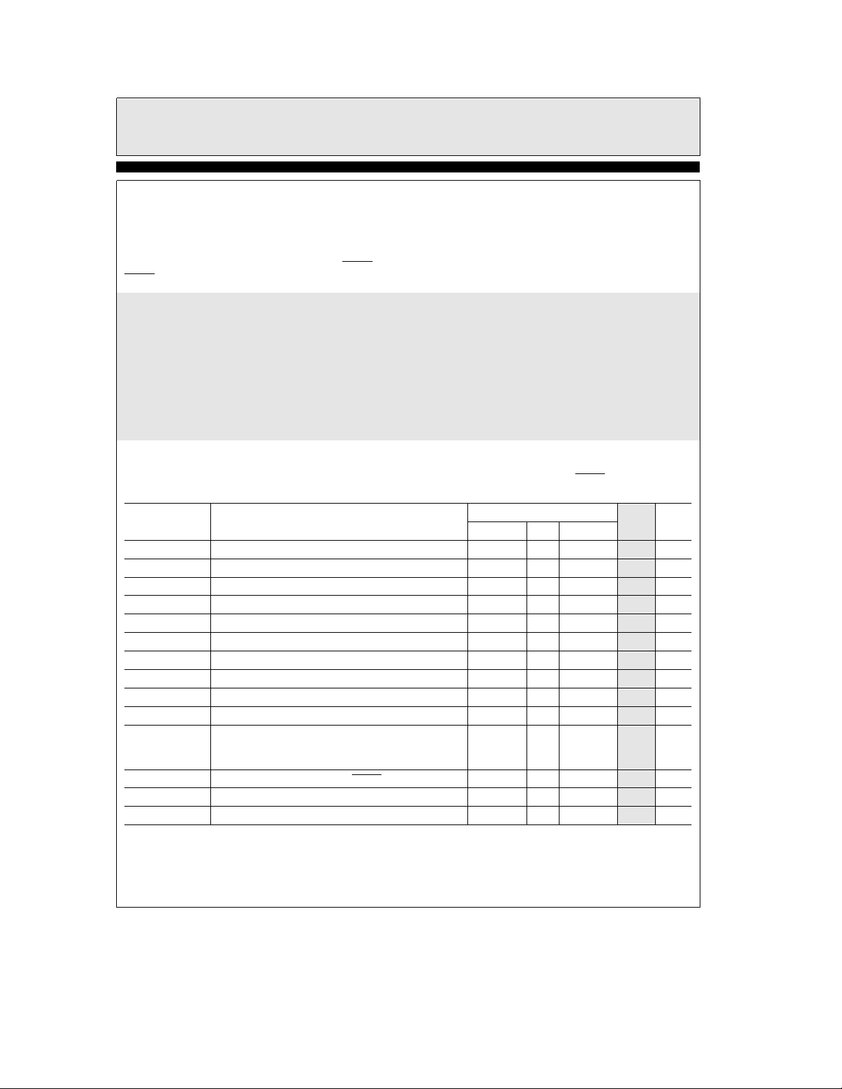
Open Loop DC Electrical Characteristics
e
g
V
S
otherwise specified
Parameter Description
V
OS
I
a
B
PSRR Power Supply Rejection Ratio 60 80 I dB
EG Gain Error, 100% Setting
V
IN
V
O
I
SC
V
GAIN
V
GAIN
NL, Gain Gain Control Non-linearity, V
NL, A
A
A
R
GAIN
I
S
F
T
5V, T
e
25§C, V
A
GAIN
ea
0.6V to measure channel A, V
Input Offset Voltage 4 30 I mV
VINInput Bias Current 2 10 I mA
VINRange (Vb)a2.5 (Va)b2.5 I V
Output Voltage Swing (Vb)a2.5 (Va)b2.5 I V
Output Short-Circuit Current 50 95 150 I mA
, 100% Minimum Voltage at V
, 0% Maximum Voltage at V
e
1 Signal Non-linearity, V
V
e
0.5 Signal Non-linearity, V
V
e
0.25 Signal Non-linearity, V
V
Resistance between V
Supply Current 12 14.5 19 I mA
Off-Channel Feedthrough
eb
GAIN
0.6V to measure channel B, V
GAIN
Limits
Min Typ Max
b
for 100% Gain 0.45 0.5 0.55 I V
GAIN
GAIN
IN
IN
IN
GAIN
for 0% Gain
e
IN
e
0tog1V, V
e
0tog1V, V
e
0tog1V, V
and V
b
g
0.5V 1.5 4 I %
e
0.55V 0.01 V %
GAIN
e
0V 0.05 V %
GAIN
eb
GAIN
GAIN
0.25V 0.2 0.5 I %
4.6 5.5 6.6 I kX
0.55
b
b
0.5
0.5
b
0.8 I %
b
0.45 I V
b
75
50 I dB
e
0V, unless
Test
Level
Units
TDis 0.6inTDis 3.3in
2
Page 3
EL4094C
Video Gain Control/Fader
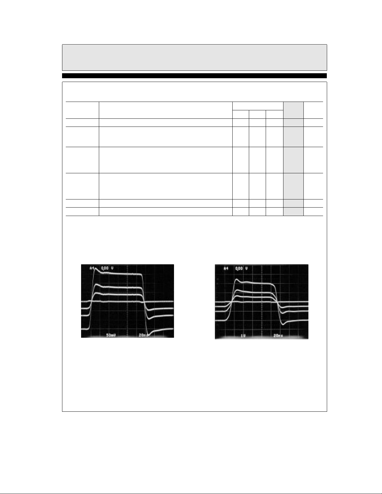
Closed Loop AC Electrical Characteristics
e
g
V
S
Parameter Description
SR Slew Rate; V
BW Bandwidth,b3 dB 45 60 III MHz
dG Differential Gain, AC amplitude of 286 mV
di Differential Phase, AC ampitude of 286 mV
BW, GAIN
T
REC
Typical Performance Curves
e
15V, C
, GAIN Gain Control Recovery from Overload; V
15 pF, T
L
at 3.58 MHz on DC offset ofb0.7, 0, anda0.7V A
at 3.58 MHz on DC offset ofb0.7, 0, anda0.7V A
b
e
A
OUT
b
b
3 dB Gain Control Bandwidth, V
e
25§C, A
1 dB 35 V MHz
0.1 dB 6 V MHz
100% unless otherwise noted
V
fromb3V toa3V measured atb2V anda2V 370 500 V V/ms
GAIN
Limits
Min Typ Max
p-p
Amplitude 0.5 V
GAIN
e
100% 0.02 V %
V
e
A
50% 0.20 V %
V
e
A
25% 0.40 V %
V
p-p
e
100% 0.04 V (§)
V
e
A
50% 0.20 V (§)
V
e
A
25% 0.20 V (§)
V
p-p
fromb0.6V to 0V 70 V ns
20 V MHz
Level
Test
Units
TDis 2.6in
Small-Signal Step
Response for Gain
25%, and 0%. V
e
100%, 50%,
g
5V
S
4094– 2
Large-Signal Step
Response for Gain
25%, and 0%. V
3
e
100%, 50%,
g
12V
S
4094– 3
Page 4
EL4094C
Video Gain Control/Fader
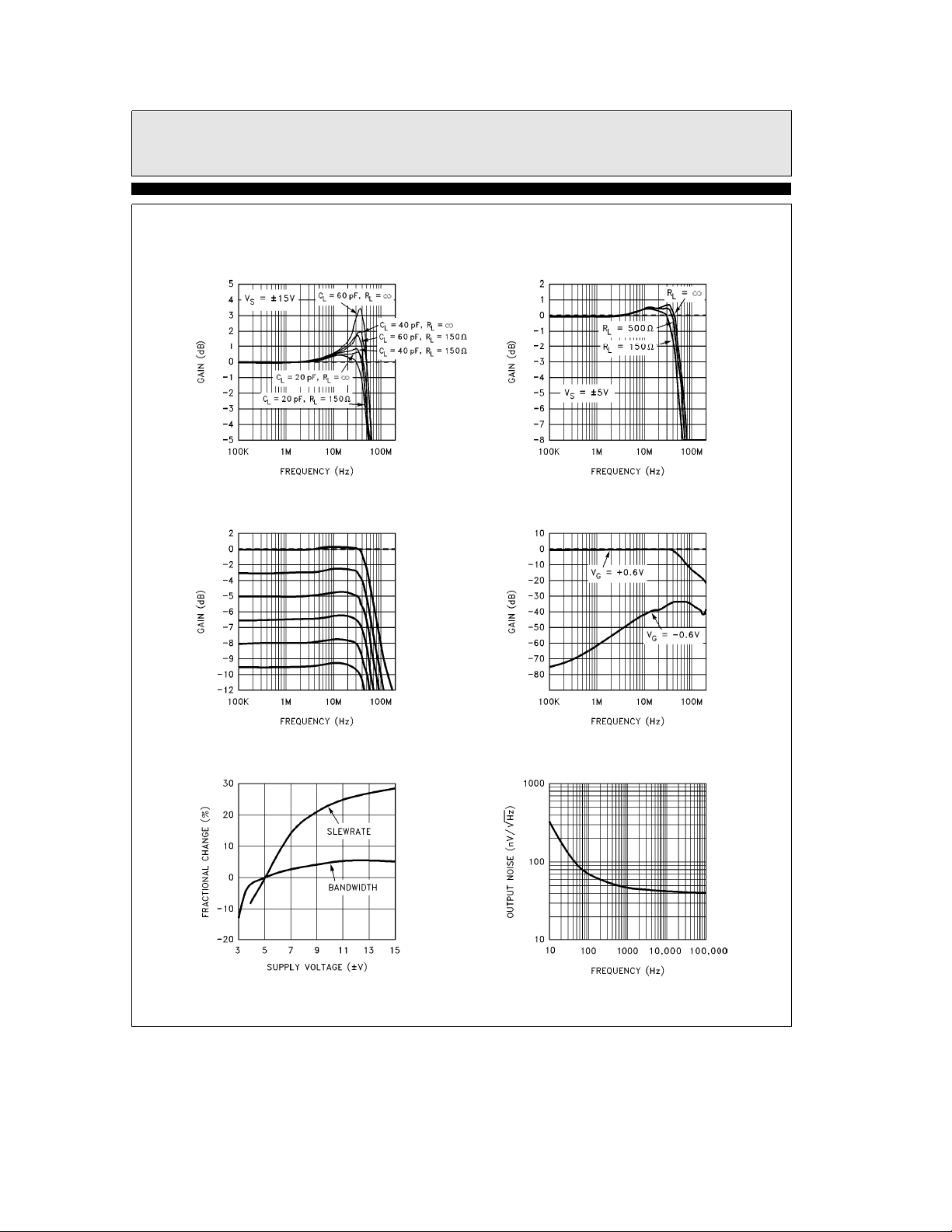
Typical Performance Curves
Frequency Response vs
Capacitive Loading
Frequency Response vs Gain Over Frequency
Ð Contd.
Frequency Response vs
Resistive Loading
Off-Channel Isolation
Change in Slewrate and
Bandwidth with Supply Voltage
Output Noise Over Frequency
4094– 4
4
Page 5

EL4094C
Video Gain Control/Fader
Typical Performance Curves
Change in 100% Gain Error,
Supply Current, Slewrate and
Bandwidth over Temperature
Differential Gain Error vs
V
for Gaine100%,
offset
75%, 50% and 25%. F
e
3.58 MHz
Ð Contd.
Nonlinearity vs V
e
Gain
100%, 75%, 50% and 25%
Differential Phase Error vs
V
for Gaine100%,
offset
75%, 50% and 25%. F
for
IN
e
3.58 MHz
Differential Gain Error vs
V
for Gaine100%,
offset
75%, 50% and 25%. F
e
3.58 MHz
Differential Phase Error vs
V
for Gaine100%,
offset
75%, 50% and 25%. F
e
3.58 MHz
4094– 5
5
Page 6

EL4094C
Video Gain Control/Fader
Typical Performance Curves
Differential Gain and
Phase Error vs Gain
Gain vs VG.1VDCat V
INA
Ð Contd.
Differential Gain and
Phase Error vs Gain
Cross-Fade Balance. V
INA
4094– 6
e
e
V
INB
0V
Gain Control Response to
a Non-Overloading Step,
Constant Sinewave at V
INA
4094– 7
4094– 9
4094– 8
V
Overload Recovery Response
GAIN
4094– 10
6
Page 7

EL4094C
Video Gain Control/Fader
Typical Performance Curves
Gain Control Gain vs Frequency Gain Control vs /VGOffset
Change in V(100%) and V(0%) of Gain
Control vs Supply Voltage
Ð Contd.
Change in V(100%) and V(0%) of
Change in V(100%) and V(0%) of Gain
Control vs Die Temperature
Supply Current vs Supply Voltage Ambient Temperature
7
Maximum Dissipation vs
4094– 11
Page 8

EL4094C
Video Gain Control/Fader
Applications Information
The EL4094 is a self-contained and calibrated
fader subsystem. When a given channel has
100% gain the circuit behaves as a current-feedback amplifier in unity-gain connection. As such,
video and transfer distortions are very low. As
the gain of the input is reduced, a 2-quadrant
multiplier is gradually introduced into the signal
path and distortions increase with reducing gain.
The input impedance also changes with gain setting, from about 1 MX at 100% gain down to
16 kX at zero gain. To maximize gain accuracy
and linearity, the inputs should be driven from
source impedances of 500X or less.
Linearity
The EL4094 is designed to work linearly with
g
2V inputs, but lowest distortion occurs atg1V
levels and below. Errors are closer to those of a
good current-feedback amplifier above 90% gain.
Low-frequency linearity is 0.1% or better for
gains 25% to 100% and inputs up to 1V. NTSC
differential gain and phase errors are better than
0.3% and 0.3
These distortions are not strongly affected by
supply voltage nor output loading, at least down
to 150X. For settling to 0.1%, however, it is best
to not load the output heavily and to run the
EL4094 on the lowest practical supply voltages,
so that thermal effects are minimized.
Gain Control Inputs
The gain control inputs are differential and may
be biased at any voltage as long as /V
than 2.5V below V
ferential input impedance is 5.5 kX, and the common-mode impedance is more than 500 kX. With
zero differential voltage on the gain inputs, both
signal inputs have a 50% gain factor. Nominal
calibration sets the 100% gain of V
a
0.5V of gain control voltage, and 0% atb0.5V
of gain control. V
that of V
at V
INB
gain. The gain control does not have a completely abrupt transition at the 0% and 100% points.
There is about 10 mV of ‘‘soft’’ transfer at the
gain endpoints. To obtain the most accurate
100% gain factor or best attenuation at 0% gain,
for the 25% to 100% gain range.
§
a
and 3V above Vb. The dif-
’s gain is complementary to
INB
;a0.5V of gain control sets 0% gain
INA
GAIN
INA
input at
andb0.5V gain control sets 100% V
is less
INB
it is necessary to overdrive the gain control input
by 30 mV or more. This would set the gain con-
b
trol voltage range as
0.565V toa0.565V, or
30 mV beyond the maximum guaranteed 0% to
100% range. In fact, the gain control inputs are
very complex. Here is a representation of the terminals:
Representation of Gain Control
Inputs V
and /V
G
G
For gain control inputs betweeng0.5V
g
(
90 mA), the diode bridge is a low impedance
and all of the current into Vg flows back out
through/V
. When gain control inputs exceed
g
this amount, the bridge becomes a high impedance as some of the diodes shut off, and the V
impedance rises sharply from the nominal 5.5KX
to about 500KX. This is the condition of gain
control overdrive. The actual circuit produces a
much sharper overdrive characteristic than does
the simple diode bridge of this representation.
The gain input has a 20 MHz
and 17 ns risetime for inputs to
b
3 dB bandwidth
g
0.45V. When
the gain control voltage exceeds the 0% or 100%
values, a 70 ns overdrive recovery transient will
occur when it is brought back to linear range. If
quicker gain overdrive response is required, the
Force control inputs of the EL4095 can be used.
Output Loading
The EL4094 does not work well with heavy capacitive loads. Like all amplifier outputs, the output impedance becomes inductive over frequency
resonating with a capacitive load. The effective
output inductance of the EL4094 is about 350
nH. More than 50 pF will cause excessive frequency response peaking and transient ringing.
The problem can be solved by inserting a lowvalue resistor in series with the load, 22X or
more. If a series resistance cannot be used, then
adding a 300X or less load resistor to ground or a
‘‘snubber’’ network may help. A snubber is a re-
8
4094– 12
g
Page 9

EL4094C
Video Gain Control/Fader
Applications Information
sistor in series with a capacitor, 150X and 100 pF
being typical values. The advantage of a snubber
is that it does not draw DC load current.
Unterminated coaxial line loads can also cause
resonances, and they should be terminated either
at the far end or a series back-match resistor installed between the EL4094 and the cable.
The output stage can deliver up to 140 mA into a
short-circuit load, but it is only rated for a continuous 35 mA. More continuous current can
cause reliability problems with the on-chip metal
interconnect. Video levels and loads cause no
problems at all.
Ð Contd.
Noise
The EL4094 has a very simple noise characteristic: the output noise is constant (40 nV/
wideband) for all gain settings. The input-referred noise is then the output noise divided by
the gain. For instance, at a gain of 50% the input
noise is 40 nV/
S
Hz/0.5, or 80 nV/SHz.
S
Hz
Bypassing
The EL4094 is fairly tolerant of power-supply
bypassing, but best multiplier performance is obtained with closely connected 0.1 mF ceramic capacitors. The leaded chip capacitors are good, but
neither additional tantalums nor chip components are necessary. The signal inputs can oscillate locally when connected to long lines or unterminated cables.
Power Dissipation
Peak die temperature must not exceed 150§C. At
this temperature, the epoxy begins to soften and
becomes unstable, chemically and mechanically.
This allows 75
75
C ambient. The EL4094 in the 8-pin PDIP
§
package has a thermal resistance of 87
can thus dissipate 862 mW at a 75
temperature. The device draws 17 mA maximum
supply current, only 510 mW at
and the circuit has no dissipation problems in
this package.
C internal temperature rise for a
§
/W, and
§
C ambient
§
g
15V supplies,
perature. The EL4094 thus cannot be operated
g
15V supplies at 75§C in the surface-mount
with
package; the supplies should be reduced to
g
to
12V levels, especially if extra dissipation oc-
curs when driving a load.
g
5V
The EL4094 as a Level Adjust
A common use for gain controls is as an input
signal levellerÐa circuit that scales too-large or
too-small signals to a standard amplitude. A typical situation would be to scale a variable video
input by
amplitude. The EL4094 cannot provide more
than 0 dB gain, but it can span the range of 0 dB
to
output up by 6 dB. The simplest way to obtain
the range is to simply ground the B input and
vary the gain of the signal applied to the A input.
The disadvantage of this approach is that linearity degrades at low gains. By connecting the signal to the A input of the EL4094 and the signal
attenuated by 12 dB to the B input, the gain control offers the highest linearity possible at 0 dB
and
tween. The circuit is shown on the following
page.
The EL4095 can be used to provide the required
gains without the extra amplifier. In practice, the
gain control is adjusted to set a standard video
level regardless of the input level. The EL4583
sync-separator has a recovered amplitude output
that can be used to servo the gain control voltage. Here is the curve of differential gain and
phase distortion for varying inputs, with the output set to standard video level:
a
6dBtob6 dB to obtain a standard
b
12 dB with another amplifier gaining the
b
12 dB extremes, and good performance be-
The SO-8 surface-mount package has a 153
thermal resistance with the EL4094, and only
490 mW can be dissipated at 75
C ambient tem-
§
/W
§
Differential Gain and Phase of
4094– 14
Linearized Level Control
9
Page 10

EL4094C
Video Gain Control/Fader
Applications Information
The differential gain error is kept to 0.3% and
the differential phase to 0.15
entire input range.
§
Ð Contd.
or better over the
The EL4094 as an Adjustable Filter
Equalizers are used to adjust the delay or frequency response of systems. A typical use is to
compensate for the high-frequency loss of a cable
system ahead of the cable so as to create a flat
response at the far end. A generalized scheme
with the EL4094 is shown below.
For an adjustable preemphasis filter, for instance,
filter A might be an all-pass filter to compensate
for the delay of filter B, a peaking filter. Fading
the gain from A to B provides a variable amount
of peaking, but constant delay.
The EL4094 as a Phase Modulator
To make a phase modulator, filter A might be a
leading-phase network, and filter B a lagging network. The wide bandwidth of the gain-control input allows wideband phase modulation of the
carrier applied to the main input. Of course, the
carrier and gain inputs must not be digital but be
reasonably clean sinewaves for the modulation to
be accurate.
a
6dBtob6 dB Linearized Level Control
General Adjustable Equalizer
10
4094– 13
4094– 15
Page 11

EL4094C
Video Gain Control/Fader
EL4094C Macromodel
This macromodel is offered to allow simulation of
general EL4094 behavior. We have included
these characteristics:
Small-signal frequency response
Output loading effects
Input impedance
Off-channel feedthrough
Output impedance over frequency
Signal path DC distortions
V
V
100% gain error
These will give a good range of results for various
operating conditions, but the macromodel does
not behave identically as the circuit in these areas:
Temperature effects
Signal overload effects
Signal and /V
Current-limit
Video and high-frequency distortions
Supply voltage effects
Slewrate limitations
Noise
Power supply interactions
The macromodel’s netlist is based on the Pspice
simulator (copywritten by the Microsim Company). Other simulators may not support the
POLY function, which is used to implement multiplication as well as square-low nonlinearities.
******
******
* V
*
*
*
*
*
.subckt EL4094subckt (1 4 6 7 8)
***
I-V characteristics
GAIN
overdrive recovery delay
GAIN
operating range
G
INB
l
ll
lll
llll
V
OUT
/V
G
V
G
V
lllll
R
810 0 290k
OL
Ccomp 810 0 3.5p
G1 10 0 810 0
R
OUT
L
OUT
RL
OUT
r1 10 910 10
c1 910 911 300p
r2 911 0 90
***
*** Input channel A
***
R
INA
ra 11 0 1k
Cfeedthrougha 23 8 130p
Rfeedthrougha 8 22 1.0
Ela 23 22 1 0 1.0
Rspice3 23 22 1E12
G1a 11 0 POLY(1) (22, 910) 0.0 0.001
G2a 810 0 POLY(2) (11,0) (13, 0) 0.0 0.0 0.0 0.0 0.001
***
***Input channel B
***
R
INB
rb 20 0 1k
Cfeedthroughb 24 1 130p
Rfeedthroughb 1 25 1.0
E1b 24 25 8 0 1.0
Rspice4 24 25 1E12
G1b 20 0 POLY(1) (25, 910) 0.0 0.001
G2b 810 0 POLY(2) (20,0) (19, 0) 0.0 0.0 0.0 0.0 0.001
***
***Gain control
***
Rspice1 13 0 1E12
Rspice2 18 0 1E12
R10 14 0 1E7
C10 14 0 8E
D1 14 15 Dclamp
D2 16 14 Dclamp
.model Dclamp D (TT
V1 15 0 4999.3
V2 0 16 4999.3
V3 13 17 0.5
V4 19 18 0.5
G1014076
INA
G1176140
E101701401E
E11180140
***
.ends
******
b
10
10 0 0.1
10 4 350.200n
10480
22 910 16k
25 910 16k
b
16
b
0.001
b2Eb
b1Eb
b
e
200n)
8
4
4
b3Eb
b3Eb
TABWIDE
6
6
TABWIDE
TDis 1.3in
TDis 6.8in
11
Page 12

EL4094C
Video Gain Control/Fader
EL4094CAugust 1996, Rev D
EL4094C Macromodel
Ð Contd.
4094– 16
EL4094 Macromodel Schematic
General Disclaimer
Specifications contained in this data sheet are in effect as of the publication date shown. Elantec, Inc. reserves the right to make changes
in the circuitry or specifications contained herein at any time without notice. Elantec, Inc. assumes no responsibility for the use of any
circuits described herein and makes no representations that they are free from patent infringement.
WARNING Ð Life Support Policy
Elantec, Inc. products are not authorized for and should not be
used within Life Support Systems without the specific written
consent of Elantec, Inc. Life Support systems are equipment in-
Elantec, Inc.
1996 Tarob Court
Milpitas, CA 95035
Telephone: (408) 945-1323
(800) 333-6314
Fax: (408) 945-9305
European Office: 44-71-482-4596
tended to support or sustain life and whose failure to perform
when properly used in accordance with instructions provided can
be reasonably expected to result in significant personal injury or
death. Users contemplating application of Elantec, Inc. products
in Life Support Systems are requested to contact Elantec, Inc.
factory headquarters to establish suitable terms & conditions for
these applications. Elantec, Inc.’s warranty is limited to replacement of defective components and does not cover injury to persons or property or other consequential damages.
Printed in U.S.A.12
 Loading...