

Page 1
EL4093C
300 MHz DC-Restored Video Amplifier
EL4093C January 1996 Rev B
Features
# High accuracy DC restoration for
video
# Low supply current of 9.5 mA
typ.
# 300 MHz bandwidth
# 1500V/ms slew rate
# 0.04% differential gain and 0.02
differential phase into 150X for
NTSC
# 1.5 mV max. restored DC offset
# Sample and hold amplifier with
fast enable and low leakage
# TTL-compatible HOLD logic
input
Applications
# Input amplifier in video
equipment
# Restoration amplifier in video
mixers
Ordering Information
Part No. Temp. Range Package Outline
EL4093CN -40§Ctoa85§C 16-pin P-DIP MDP0031
EL4093CS -40§Ctoa85§C 16-Lead SOIC MDP0027
General Description
The EL4093C is a complete DC-restored video amplifier subsystem, featuring low power consumption and high slew rate. It
contains a current feedback amplifier and a sample and hold
amplifier designed to stabilize video performance. When the
HOLD logic input is low, the sample and hold may be used as a
general purpose op amp to null the DC offset of the video amplifier. When the HOLD input goes high the sample and hold
§
stores the correction voltage on the hold capacitor to maintain
DC correction during the subsequent video scan line.
The sample and hold amplifier contains a current output stage
that greatly simplifies its connection to the video amplifier. Its
high output impedance also helps to preserve video linearity at
low supply voltages. For ease of interfacing, the HOLD input is
TTL-compatible. This device has an operational temperature of
b
40§Ctoa85§C and is packaged in plastic 16-pin DIP and 16-
lead SOIC.
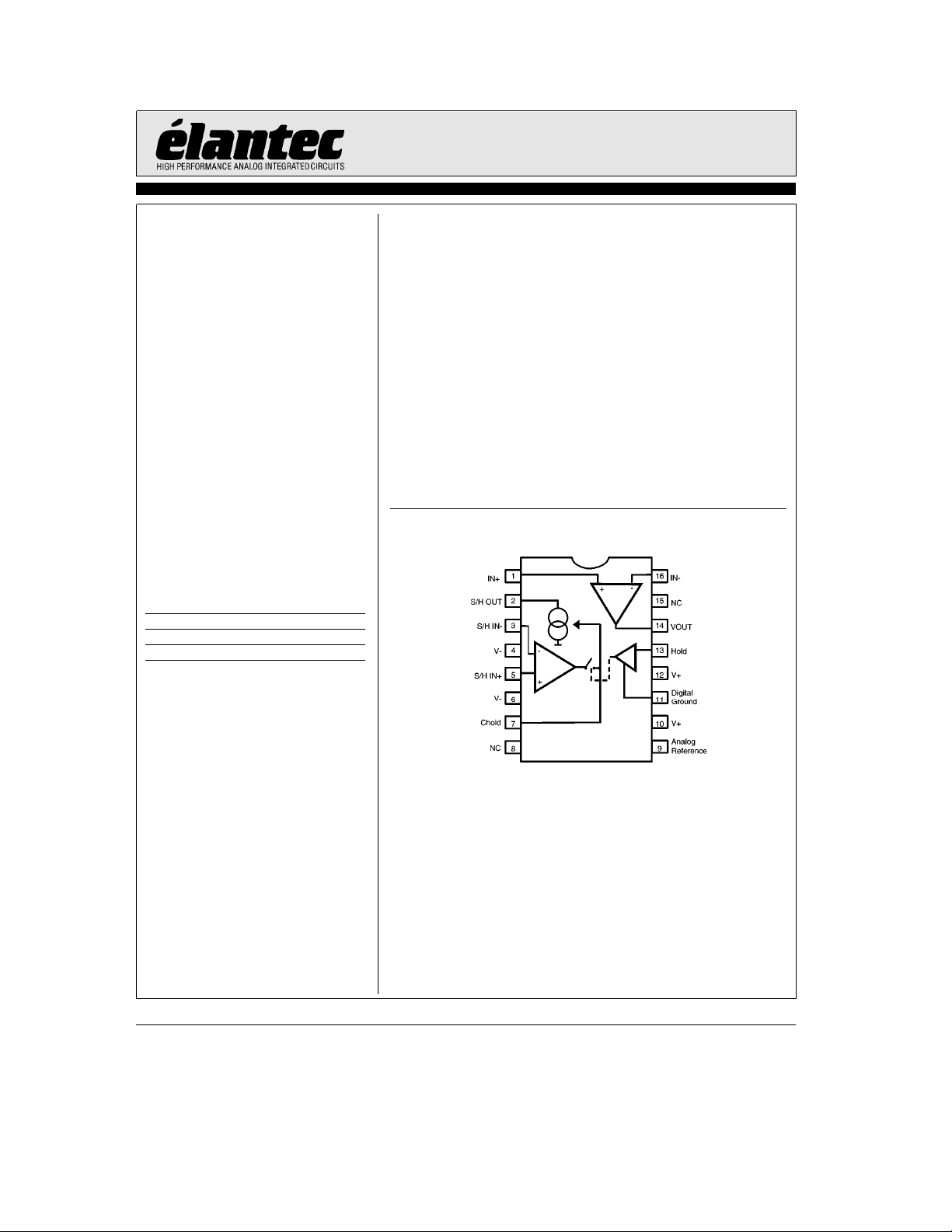
Connection Diagram
Ý
Demo Board
A demo PCB is available for this
product. Request ‘‘EL4093 Demo
Board.’’
44093– 1
Note: All information contained in this data sheet has been carefully checked and is believed to be accurate as of the date of publication; however, this data sheet cannot be a ‘‘controlled document’’. Current revisions, if any, to these
specifications are maintained at the factory and are available upon your request. We recommend checking the revision level before finalization of your design documentation.
©
1995 Elantec, Inc.
Page 2
EL4093C
300 MHz DC-Restored Video Amplifier
Absolute Maximum Ratings
g
g
b
65§Ctoa150§C
e
TA.
C
Units
Units
10 mA
6mA
8V
I
S/H amplifier output current
OUT2
I
Maximum current into other pins
IN
P
Maximum Power Dissipation See Curves
D
b
T
Operating Ambient Temperature Rangeb40§Ctoa85§C
A
T
Operating Junction Temperature 150§C
J
T
Storage Temperature Range
ST
e
T
J
e
25§C,
A
Power supplies atg5V, T
e
25§C
A
Test
Level
V
Vato VbSupply Voltage 12.6V
S
V
Voltage at HOLD input
HOLD
V
Voltage at any other input Vato V
IN
DVINDifference between Sample and Hold inputs
I
Video amplifier output current
OUT1
Important Note:
All parameters having Min/Max specifications are guaranteed. The Test Level column indicates the specific device testing actually
performed during production and Quality inspection. Elantec performs most electrical tests using modern high-speed automatic test
equipment, specifically the LTX77 Series system. Unless otherwise noted, all tests are pulsed tests, therefore T
Test Level Test Procedure
I 100% production tested and QA sample tested per QA test plan QCX0002.
II 100% production tested at T
III QA sample tested per QA test plan QCX0002.
IV Parameter is guaranteed (but not tested) by Design and Characterization Data.
V Parameter is typical value at T
T
MAX
and T
b
(DGND
0.7) to (DGNDa5.5V)
per QA test plan QCX0002.
MIN
g
g
30 mA
e
25§C and QA sample tested at T
A
e
25§C for information purposes only.
A
Open-Loop DC Electrical Characteristics
Parameter Description Min Typ Max
I
S,HOLD
I
S,SAMPLE
Total Supply current in HOLD mode 9.5 11.5 I mA
Total Supply current in SAMPLE mode 8.5 10.5 I mA
Video Amplifier Section (Not Restored)
Parameter Description Min Typ Max
V
OS
I
a
B
I
b
B
R
OL
V
O
I
SC
Input Offset Voltage 10 110 I mV
Non-Inverting Input Bias Current 10 25 I mA
Inverting Input Bias Current 15 50 I mA
Transimpedance
e
g
V
OUT
Output Voltage Swing
e
R
150X
L
2.5V, R
e
150X 150 400 I kX
L
g
3
g
3.5 I V
Output Short-Circuit Current 60 100 I mA
Test
Level
TABWIDE
TDis0.7in
TDis1.7in TDis1.7in
2
Page 3
EL4093C
300 MHz DC-Restored Video Amplifier
Open-Loop DC Electrical Characteristics
Power supplies atg5V, T
Sample and Hold Section
Parameter Description Min Typ Max
V
OS
TCV
OS
I
B
I
OS
TCI
OS
V
CM
g
m
CMRR Common Mode Rejection Ratio (V
V
IL
V
IH
V
GND
I
DROOP
I
CHARGE
V
O
I
O
Input Offset Voltage 0.5 1.5 I mV
Average Offset Voltage Drift 6 V mV/§C
Input Bias Current 1 2 I mA
Input Offset Current 10 200 I nA
Average Offset Current Drift 0.1 V nA/§C
Common Mode Input Range
Transconductance (R
HOLD Logic Input Low (referenced to Digital GND) 0.8 I V
HOLD Logic Input High (referenced to Digital GND) 2.0 I V
Digital GND Reference Voltage (Vb)(V
Hold Mode Droop Current 10 70 I nA
Charge Current Available to C
Output Voltage Swing (R
Output Current Swing (R
e
25§C Ð Contd.
A
g
g
2.5
2.8 I V
e
500X) 5 15 I A/V
L
b
2.5V toa2.5V) 70 90 I dB
CM
g
g
5.5
HOLD
e
10kX)
L
e
0X)
L
g
g
8.5 I mA
g
3
3.5 I V
g
4.5
5.5 I mA
Closed-Loop AC Electrical Characteristics
Power supplies atg5V, T
e
25§C, R
A
e
e
R
G
750X,R
F
L
e
150X,C
e
5 pF, C
L
(parasitic)e1.8 pF
b
IN
a
b
)
4.0 I V
Test
Level
Units
Video Amplifier Section
Parameter Description Min Typ Max
BW,b3dB
b
3 dB Small-Signal Bandwidth 300 V MHz
BW,g0.1 dB 0.1 dB Flatness Bandwidth 50 V MHz
Peaking Frequency Response Peaking 0 V dB
SR Slew rate, V
betweenb2V anda2V 1500 V V/ms
OUT
dG Differential Gain Error, Voffset betweenb714 mV anda714 mV 0.04 V %
di Differential Phase Error, Voffset betweenb714 mV anda714 mV 0.02 V
3
Test
Levels
Units
§
TDis1.5in TDis1.5in
Page 4
EL4093C
300 MHz DC-Restored Video Amplifier
Closed-Loop AC Electrical Characteristics
Power supplies atg5V, T
e
25§C, R
A
Sample and Hold Section
Parameter Description Min Typ Max
DI
DT
DT
T
STEP
SH
HS
AC
Change in Sample to Hold Output Current Due to Hold Step 0.1 V mA
Sample to Hold Delay Time 15 V ns
Hold to Sample Delay Time 40 V ns
Settling Time to 1% (DC Restored Amplifier Output) 2.2 V ms
Video Amplifier Input from 0 to 1V
e
e
R
G
750X,R
F
L
e
150X,C
e
5 pF, C
L
HOLD
e
2.2 nF
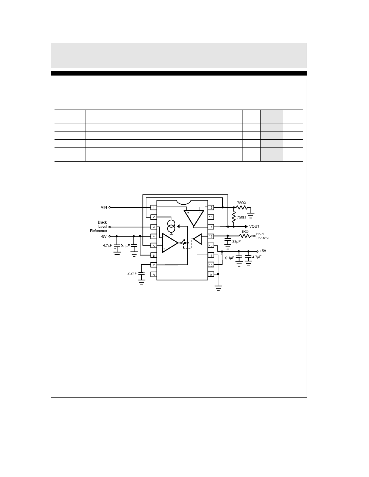
Typical Application
Test
Levels
Units
TDis1.2in
44093– 2
4
Page 5
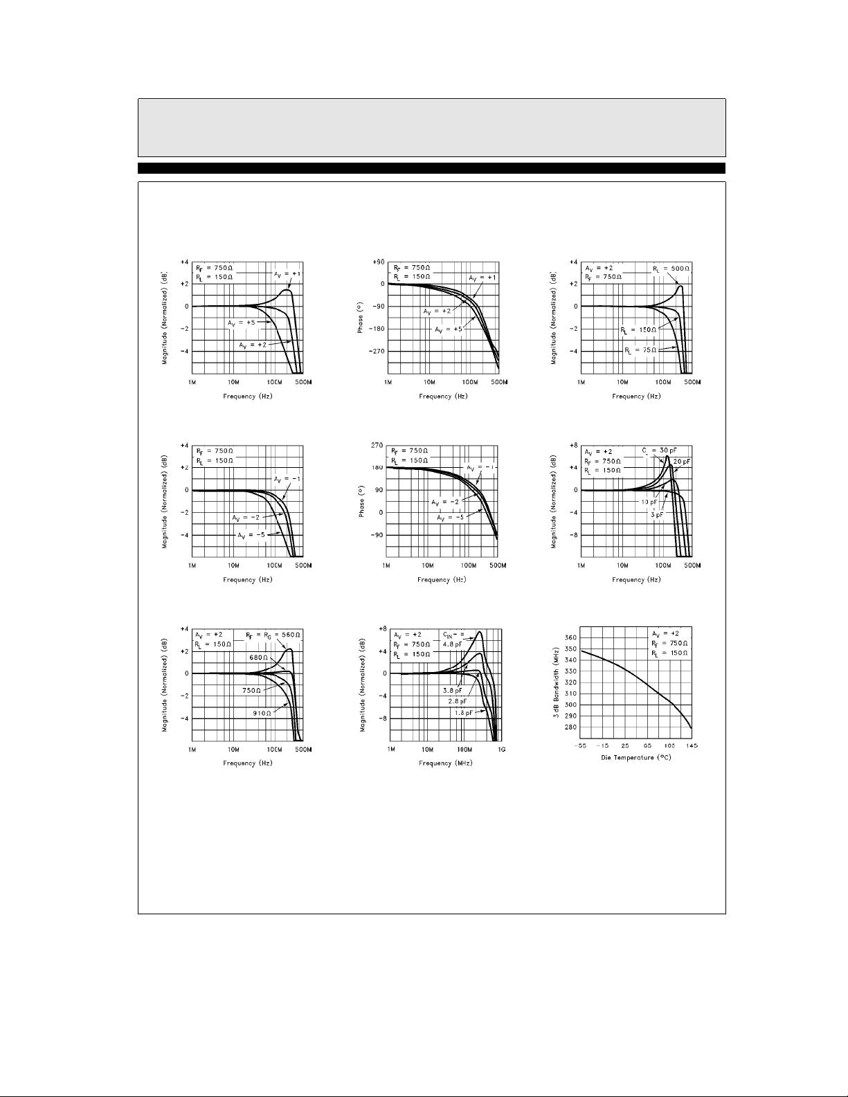
Typical Performance Curves
EL4093C
300 MHz DC-Restored Video Amplifier
Non-inverting Frequency
Response (Gain)
Inverting Frequency
Response (Gain)
Frequency Response for
Various RFand R
G
44093– 4
44093– 7
Non-inverting Frequency
Response (Phase)
Inverting Frequency
Response (Phase)
Frequency Response
for Various C
IN
44093– 5
44093– 8
Frequency Response
for Various R
Frequency Response
for Various C
3 dB Bandwidth vs
Temperature (Video Amp)
L
L
44093– 6
44093– 9
44093– 10
44093– 11
44093– 12
5
Page 6

EL4093C
300 MHz DC-Restored Video Amplifier
Typical Performance Curves
Peaking vs Temperature
(Video Amp)
44093– 13
Voltage and Current
Noise vs Frequency
Input Offset Voltage
vs Die Temperature
(Video Amp, 3 Sample)
Ð Contd.
Output Voltage
Swing vs Frequency
44093– 16
Input Bias Current vs
Temperature (Video Amp)
44093– 14
2nd and 3rd Harmonic
Distortion vs Frequency
Supply Current
vs Temperature
Transimpedance vs
Temperature (Video Amp)
44093– 15
44093– 17
44093– 18
44093– 19
44093– 20
6
Page 7

EL4093C
300 MHz DC-Restored Video Amplifier
Typical Performance Curves
Input Offset Voltage
vs Die Temperature
(Sample & Hold, 3 Samples)
44093– 21
Transconductance vs
Die Temperature
(Sample & Hold)
Droop Current
vs Temperature
(Sample & Hold)
Ð Contd.
Input Bias Current vs
Die Temperature
(Sample & Hold)
44093– 38
Charge Current vs
Temperature
(Sample & Hold)
44093– 22
Transconductance vs
Temperature (Sample & Hold)
Output Current Swing vs
Temperature (Sample & Hold)
Hold Step (DI
vs Temperature
OUT
44093– 23
44093– 25
)
44093– 26
44093– 27
44093– 28
7
Page 8

EL4093C
300 MHz DC-Restored Video Amplifier
Typical Performance Curves
Differential Gain and
Phase vs DC Input
Voltage at 3.58 MHz
44093– 29
Small-Signal Step Response
Ð Contd.
Differential Gain and
Phase vs DC Input
Voltage at 3.58 MHz
Slew Rate vs Die
Temperature (Video Amp)
44093– 30
Large-Signal Step Response
44093– 31
Settling Time vs
Settling Accuracy
(Video Amp)
44093– 34
44093– 32
Maximum Power Dissipation
vs Ambient Temperature,
16-Pin P-DIP Package
44093– 35
8
44093– 33
Maximum Power Dissipation
vs Ambient Temperature,
16-Pin SO Package
44093– 36
Page 9

300 MHz DC-Restored Video Amplifier
Applications Information
Product Description
The EL4093C is a high speed DC-restore system
containing a current feedback amplifier (CFA)
and a sample & hold (S/H) amplifier. The CFA
offers a wide 3 dB bandwidth of 300 MHz and a
slew rate of 1500 V/ms, making it ideal for high
speed video applications such as SVGA. The
CFA’s excellent differential gain and phase at
3.58 MHz also makes it suitable for NTSC applications. Drawing only 9.5 mA on
the EL4093C serves as an excellent choice for
those applications requiring both low power and
high bandwidth.
The connection between the CFA and sample &
hold (the Autozero interface) has been greatly
simplified. The output of the sample & hold is a
high impedance current source, allowing direct
connection to the CFA inverting input for autozero purposes. In addition, special circuitry
within the sample & hold provides a charge current of 8.5 mA in sample mode, resulting in a
sample hold current ratio (ratio of charging current to droop current) of approx. 1,000,000.
Theory of Operation
In video applications, DC restoration moves the
backporch or black level to a fixed DC reference.
The EL4093C uses a CFA in feedback with a
sample & hold to provide DC restoration. Figure
1 shows how the two are connected to provide
this function; the S/H compares the output of
the CFA to a DC reference, and any difference
between them causes an output current from the
S/H. This ‘‘autozero’’ current is fed to the CFA
inverting input, the effect of which is to move the
CFA output towards the reference voltage. This
autozero mechanism settles when the CFA output is one V
here refers to the S/H offset voltage).
away from the reference (the V
OS
g
5V supplies,
OS
EL4093C
Figure 1
The autozero mechanism is typically active for
only a short period of each video line. Figure 2
shows a NTSC video signal along with the
EL4581C back porch output. The back porch signal is used to drive the HOLD input of the
EL4093C, and we see that the EL4093C is in
sample mode for only 3.5 ms of each line. It is
during this time that the autozero mechanism attempts to drive the CFA output towards the reference voltage, at the same time putting a correction voltage onto the hold capacitor C
During the rest of the line (60 ms) the EL4093C is
in hold mode, but DC correction is maintained by
the voltage on C
HOLD
.
44093– 3
HOLD
.
Figure 2
9
44093– 37
Page 10

EL4093C
300 MHz DC-Restored Video Amplifier
Applications Information
Ð Contd.
Power Supply Bypassing and Printed
Circuit Board Layout
As with any high frequency device, good printed
circuit board layout is necessary for optimum
performance. Ground plane construction is highly recommended. Lead lengths should be as short
as possible. The power supply pins must be well
bypassed to reduce the risk of oscillation. In the
EL4093C there are two sets of supply pins:
a
V
1/Vb1 provide power for the CFA, and
a
V
2/Vb2 are for the S/H amplifier. Good performance can be achieved using only one set of
bypass capacitors, although they must be close to
a
the V
1/V-1 pins since that is where the high
frequency currents flow. The combination of a
4.7 mF tantalum capacitor in parallel with a
0.01 mF capacitor has been shown to work well.
Chip capacitors are recommended for the 0.01 mF
bypass to minimize lead inductance.
For good AC performance, parasitic capacitance
should be kept to a minimum, especially at the
CFA inverting input. Ground plane construction
should be used, but it should be removed from
the area near the inverting input to minimize any
stray capacitance at that node. Chip resistors are
recommended for R
and RG, and use of sockets
F
should be avoided if possible. Sockets add parasitic inductance and capacitance which will result
in some additional peaking and overshoot.
If the CFA is configured for non-inverting gain,
then one should also pay attention to the trace
leading to the
l
trace (
a
input. The inductance of a long
3’’) can form a resonant network with
the amplifier input, resulting in high frequency
oscillations around 700 MHz. In such cases a
50X– 100X series resistor placed close to the
a
input would isolate this inductance and damp out
the resonance.
Capacitance at the Inverting Input
Any manufacturer’s high-speed voltage or current feedback amplifier can be affected by stray
capacitance at the inverting input. For inverting
gains this parasitic capacitance has little effect
because the inverting input is a virtual ground,
but for non-inverting gains this capacitance (in
conjunction with the feedback and gain resistors)
creates a pole in the feedback path of the amplifier. This pole, if low enough in frequency, has the
same destabilizing effect as a zero in the forward
open-loop response. Hence it is important to minimize the stray capacitance at this node by removing the nearby ground plane. In addition,
since the S/H output connects to this node, it is
important to minimize the trace capacitance.
Good practice here would be to connect the two
pins with a short trace directly underneath the
chip.
Feedback Resistor Values
The EL4093C has been optimized for a gain of
a
2 with R
e
750X. This value of feedback re-
F
sistor givesa3dBbandwidth of 300 MHz at a
gain of
a
2 driving a 150X load. Since the ampli-
fier inside the EL4093C uses current mode feedback, it is possible to change the value of R
to
F
adjust the bandwidth. Shown in the table below
are optimum feedback resistor values for different closed loop gains.
Gain Optimum RF BW (MHz) Peaking (dB)
a
1 910 314 0.2
a
2 750 300 0
a
5 470 294 0.2
b
1 680 300 0
Autozero Interface
The autozero interface refers to the connection
between the S/H output and the CFA inverting
input. This interface has been greatly simplified
compared to that of the EL2090C, in that the
S/H output is a high impedance current source.
The S/H output can be connected directly to the
inverting input, and its high impedance greatly
reduces the interaction between the sample &
hold and the gain setting resistors. Another virtue of this interface is better gain linearity as the
autozero current changes. For example, at an autozero current of 0 mA the output impedance is
about 5 MX, dropping to 1 MX as the autozero
e
current increases to 3 mA. Using R
F
e
R
G
750X, the closed loop gain changes only by
0.025% in this interval.
10
Page 11

EL4093C
300 MHz DC-Restored Video Amplifier
Applications Information
Ð Contd.
Autozero Range
The autozero range is defined as the difference
between the input DC level and the reference
voltage to restore to. The size of this range is a
function of the gain setting resistors used and the
S/H output current swing. For a gain of
a
2 the
optimum feedback resistor is 750X, and the available S/H output current is
g
5.5 mA minimum.
To determine the autozero range for this case, we
refer to Figure 3 below.
Figure 3
4093– 39
Suppose that the input DC level isaVDC, and
that the reference voltage is 0V. We know that in
feedback, the following two conditions will exist
on the CFA: first, its output will be equal to 0V
AZ
IN
b
e
voltage
be
IN
(I
RF
a
(due to autozero), and second, its V
is equal to the V
a
VDC). So we have a potential difference of
a
VDCacross both RFand RG, resulting in a cur-
rent I
RF
e
I
RG
a
voltage (i.e. V
IN
e
VDC/750X that must flow
into each of them. This current I
IRG) must come from the S/H output. Since the
maximum that I
for V
using the following:
DC
can be is 5.5 mA, we can solve
AZ
As another example, consider the case where we
a
RF
0.75V.
a
I
RF
RG
are restoring to a reference voltage of
Using the same reasoning as above, a current I
e
and a current I
(V
b
0.75V)/RFmust flow through RF,
DC
e
VDC/RGmust go into RG.
RG
Again, our boundary condition is that I
s
g
5.5 mA, and we can solve for the allowable
V
values using the following:
DC
b
g
5.5 mA
Hence V
V
e
must be betweena2.4V tob1.7V.
DC
DC
750X
0.75V
a
V
DC
750X
This example illustrates that when the reference
changes, the autozero range also changes. In general, the user should determine the autozero
range for his/her application, and ensure that the
input signal is within this range during the autozero period.
Autozero Loop Bandwidth
The gain-bandwidth product (GBWP) of the autozero loop is determined by the size of the hold
capacitor, the value of R
, and the transconduct-
F
ances (gm’s) of the S/H amplifier. To begin, the
S/H amplifier is modeled as in Figure 4 below.
First, the input stage transconductance is represented by gm1, with the compensation capacitor
given by C
gm1/(2
q
e
#
207 kHz. Next, since the S/H has a current
. This stage’s GBWP is thus
HOLD
C
)e1/(2q#(350X)(2.2 nF))
HOLD
output, its output stage can be modeled as a
transconductance gm2, in this case having a value of 1/(500X). The current from gm2 then flows
through the I to V converter made up of the CFA
and R
to produce a voltage gain. Thus the
F
GBWP of the overall loop is given by:
gm1
GBWP
e
2q#C
(gm2#RF)
HOLD
V
e
g
I
AZ
5.5 mAe2
and see that V
DC
DC
750X
#
J
e
g
2V. This range can easily
accommodate most video signals.
11
Page 12

EL4093C
300 MHz DC-Restored Video Amplifier
Applications Information
With R
tained. Note however that this is the small signal
GBWP. As mentioned earlier, the sample and
hold has special boost circuits built in which provides
These boost circuits turn on when the S/H input
differential voltage exceeds
boosters are turned on, gm1 greatly increases and
the circuit becomes nonlinear. Thus some stability issues are associated with the boosters, and
they will be addressed in a later section.
e
750X, a GBWP of 310 kHz is ob-
F
g
8.5 mA of charge current during full slew.
g
Ð Contd.
50 mV. When the
Charge Injection and Hold Step
Charge injection refers to the charge transferred
to the hold capacitor when switching to the
HOLD mode. The charge should ideally be 0, but
due to stray capacitive coupling and other effects,
is typically 0.1 pC in the EL4093. This charge
changes the hold capacitor voltage by DV
C
stage transconductance (gm2) to produce a
change in S/H output current. This last quantity
is listed as the spec DI
ing the following:
DI
, and this DV is multiplied by the output
HOLD
, and is calculated us-
STEP
DQ
STEP
e
#
C
HOLD
gm2
#
J
e
DQ/
Figure 4
e
For C
HOLD
DI
change in S/H output current flows through R
shifting the CFA output voltage. However, as we
shall soon see, this shift is negligible. Assuming
R
F
give (750X)(100 nA)
CFA output.
has a typical value of 100 nA. This
STEP
e
750X, DI
2.2 nF and gm2e1/(500X),
STEP
4093– 40
is impressed across RFto
e
0.08 mV of change at the
Droop Rate
When the S/H amplifier is in HOLD mode, there
is a small current that leaks from the switch into
the hold capacitor. This quantity is termed the
droop current, and is typically 10 nA in the
EL4093. This droop current produces a ramp in
the hold capacitor voltage, which in turn produces a similar effect at the CFA output. The Droop
Rate at the CFA output can be found using the
equation below:
I
DROOP
e
Droop
Assuming R
drift in the CFA output due to droop current is
about 7 mV/ms. Recall that in NTSC applications, there is about 60 ms between autozero periods. Thus there is 7 mV/ms)(60 ms)
less than 0.1 IRE, of drift over each NTSC scan
line. This drift is negligible in most applications.
12
C
HOLD
e
F
(gm2#RF)
750X and C
HOLD
e
2.2 nF, the
e
0.4 mV, or
,
F
Page 13

EL4093C
300 MHz DC-Restored Video Amplifier
Applications Information
Ð Contd.
Choice of Hold Capacitor
The EL4093 has been designed to work with a
hold capacitor of 2.2 nF. With this value of
C
, the droop rate and hold step are negligi-
HOLD
bly small for most applications. In addition, with
the special boost circuits inside the S/H, fast acquisition is possible even using a hold capacitor
of this size. Figure 5 below shows the input and
output of the DC-restored amplifier while the
S/H is in sample mode. Applying a
a
1V step to
the non-inverting input of the CFA, the output
of the CFA jumps to
a
2V. The S/H, however,
then tries to autozero the system by driving the
CFA output back to the reference voltage. Since
the input differential across the S/H is initially
a
2V, the boost circuits turn on and supply
8.5 mA of charge current to the hold capacitor.
The boost circuit remains on until the CFA output has come to within 50 mV of the reference.
Note that this event took only 320 ns; settling to
within 1% of the final value takes another 2 ms.
Thus for a 1V input step, acquisition takes only
one to two NTSC scan lines.
In the other direction, decreasing C
HOLD
would
increase the droop and hold step but shorten the
acquisition time. There is, however, a caveat to
reducing C
: too small a C
HOLD
HOLD
would
cause the autozero loop to oscillate. The reason is
that when the S/H boost circuit turns on, the
input stage gm increases drastically and the circuit becomes nonlinear. A sufficiently large
C
must be used to suppress the non-lineari-
HOLD
ty and force the loop to settle. For example, it
has been found that a C
1V
oscillation around 10 MHz at the CFA
P-P
of 470 pF results in
HOLD
output.
The minimum recommended value for C
HOLD
2.2 nF. With this value the loop remains stable
over the entire operating temperature range
b
(
40§Ctoa85§C). The greatest instability occurs at low temperatures, where we observe from
the performance curves that the S/H gm’s, and
hence the GBWP, are at their maximum. If the
operating range is restricted to room temperature
or above, then 1.5 nF is sufficient to keep the
loop stable. At this value of C
HOLD
the acquisi-
tion time reduces to about 1.5 ms.
Video Performance and Application
Although the EL4093 is intended for high speed
video applications such as SVGA, it also offers
excellent performance for NTSC, with 0.04% dG
and 0.02
dP at 3.58 MHz. Some application con-
§
siderations, however, are required for handling
NTSC signals.
is
Figure 5. Autozero Mechanism Restores
Amplifier Output to Ground
aftera1V Step at Input
4093– 41
A natural question arises as to whether there are
other C
rection, increasing C
values that can be used. In one di-
HOLD
will further reduce the
HOLD
droop and hold step, but lengthen the acquisition
time. Since the droop and hold step are already
small to begin with, there is no apparent advantage to increasing C
HOLD
.
Referring back to Figure 2, recall that typically,
the autozero interval lies in the back porch portion of video containing the colorburst pulse.
When the S/H compares the video to the reference voltage during this period, the colorburst
(40 IRE
) triggers the S/H boost circuit and
P-P
prevents the autozero loop from settling.
13
Page 14

EL4093C
300 MHz DC-Restored Video Amplifier
Applications Information
Ð Contd.
A remedy for this situation is to attenuate the
colorburst before applying it to the S/H input.
Figure 6 below shows a 3.58 MHz chroma trap
which would notch out the colorburst while preserving the video DC level.
Figure 6. Colorburst Trap for NTSC Applications
4093– 42
One may be tempted to use a RC lowpass filter to
suppress the colorburst, as shown in Figure 7 below. This technique, however, poses several problems. First, to obtain enough attenuation, we
need to set the pole frequency 10 to 20 times lower than 3.58 MHz. This pole, being close to the
auto zero loop pole, would destabilize the system
and cause the loop to oscillate.
Figure 7. Caution: Lowpass Filter Does Not
4093– 43
Work in NTSC Applications
Although we can cancel this pole by introducing
a zero, the RC network introduces a time delay
between the CFA output and the S/H input. This
has undesirable effects in some NTSC applications, as Figure 8 below illustrates. There is only
0.6 ms from the rising edge of sync to the colorburst. If we are autozeroing over the back porch,
the autozero period would begin somewhere in
this 0.6 ms interval. Since the edge of sync is now
delayed by the RC network, autozero begins before the video back porch reaches its final value.
Consequently, the autozero loop performs a correction on every line and never settles.
Figure 8. Lowpass Filter Delays Input to Sample and Hold
14
4093– 44
Page 15

EL4093C
300 MHz DC-Restored Video Amplifier
Applications Information
Ð Contd.
If the video does not contain any AC components
during the autozero level (e.g. RGB video), then
the above networks are not needed and the CFA
output can be connected directly to the S/H input.
Power Dissipation
The EL4093 current feedback amplifier has an
absolute maximum of
g
30 mA output current
drive. This is slightly more than the current required to drive
g
2V into 75X. To see how much
the junction temperature is raised in this worst
case, we refer to the equations below:
T
JMAX
e
T
MAX
a
(i
JA
PD
#
MAX
)
where:
MAX
e
Maximum Ambient Temperature
e
Thermal Resistance of the Package
e
Maximum Power Dissipation of the
T
i
PD
MAX
JA
CFA and S/H amplifier in the Package
PD
for either the CFA or the S/H amplifier
MAX
can be calculated as follows:
e
PD
MAX
(2#V
a
(V
S
S
b
I
#
SMAX
V
OUTMAX
)
)#(V
OUTMAX/RL
)
where:
V
S
I
SMAX
e
Supply Voltage
e
Maximum Supply Current of
Amplifier
V
OUTMAX
e
Maximum Output Voltage of
Application
R
L
e
Load Resistance
For the EL4093, the maximum supply current is
e
11.5 mA on V
case, the CFA output swings
g
5V. Assume that in the worst
S
g
2V into 75X.
Since the S/H has a current output, we assume
that it is at maximum current swing (
g
5.5 mA)
but at a mid-rail output voltage (0V). With the
above assumptions, PD
for the EL4093 is
MAX
223 mW, and using the thermal resistance of a
narrow SO package (120
perature increase of 27
ambient temperature is 85
tion temperature of 112
C/W), this yields a tem-
§
C. Since the maximum
§
C, the resulting junc-
§
C is still below the maxi-
§
mum.
Please note that there is no short-circuit protection on the EL4093 CFA output, and hence the
minimum short circuit current (60 mA) is greater
than the absolute maximum output current.
Maintaining the EL4093 in this state for more
than a few seconds may cause the part to exceed
T
, in addition to metal migration problems.
JMAX
15
Page 16

EL4093C
300 MHz DC-Restored Video Amplifier
EL4093CJanuary 1996 Rev B
General Disclaimer
Specifications contained in this data sheet are in effect as of the publication date shown. Elantec, Inc. reserves the right to make changes
in the circuitry or specifications contained herein at any time without notice. Elantec, Inc. assumes no responsibility for the use of any
circuits described herein and makes no representations that they are free from patent infringement.
WARNING Ð Life Support Policy
Elantec, Inc. products are not authorized for and should not be
used within Life Support Systems without the specific written
consent of Elantec, Inc. Life Support systems are equipment in-
Elantec, Inc.
1996 Tarob Court
Milpitas, CA 95035
Telephone: (408) 945-1323
(800) 333-6314
Fax: (408) 945-9305
European Office: 44-71-482-4596
tended to support or sustain life and whose failure to perform
when properly used in accordance with instructions provided can
be reasonably expected to result in significant personal injury or
death. Users contemplating application of Elantec, Inc. products
in Life Support Systems are requested to contact Elantec, Inc.
factory headquarters to establish suitable terms & conditions for
these applications. Elantec, Inc.’s warranty is limited to replacement of defective components and does not cover injury to persons or property or other consequential damages.
Printed in U.S.A.16
 Loading...