

Page 1
EL4089C
DC Restored Video Amplifier
EL4089C January 1996 Rev B
Features
# Complete video level restoration
system
# 0.02% differential gain and 0.05
differential phase accuracy at
NTSC
# 60 MHz bandwidth
# 0.1 dB flatness to 10 MHz
e
S
g
5V tog15V
# V
# TTL/CMOS hold signal
Applications
# Input amplifier in video
equipment
# Restoration amplifier in video
mixers
Ordering Information
Part No. Temp. Range Package Outline
EL4089CN 0§Ctoa75§C 8-Pin P-DIP MDP0031
EL4089CS 0§Ctoa75§C 8-Lead SO MDP0027
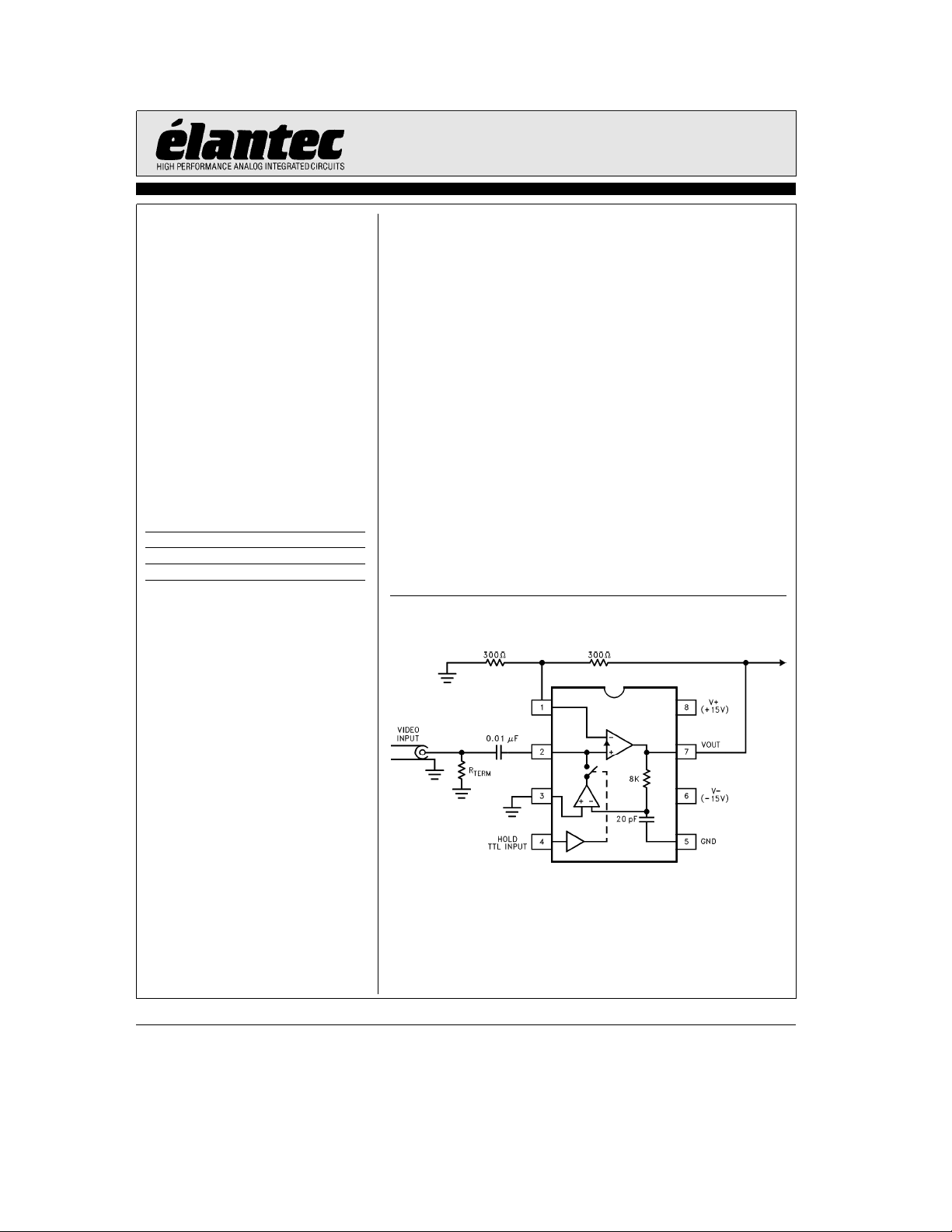
General Description
The EL4089C is an 8-pin complete DC-restored monolithic video amplifier sub-system. It contains a high quality video amplifier and a nulling, sample-and-hold amplifier specifically de-
§
signed to stabilize video performance.
When the HOLD logic input is set to a TTL/CMOS logic 0, the
sample- and-hold amplifier can be used to null the DC offset of
the video amplifer.
When the HOLD input goes to a TTL/CMOS logic l, the correcting voltage is stored on the video amplifier’s input coupling
capacitor. The correction voltage can be further corrected as
need be, on each video line.
The video amplifier is optimized for video performance and low
power. Its current feedback design allows the user to maintain
essentially the same bandwidth over a gain range of nearly 10:1.
The amplifier drives back-terminated 75X lines.
The EL4089C is fabricated in Elantec’s proprietary Comple-
Ý
mentary Bipolar process which produces NPN and PNP transistors with equivalent AC and DC performance. The EL4089C
is specified for operation over 0
Ctoa75§C temperature range.
§
Connection Diagram
DC restoring amplifier with a gain of 2, restoring to ground.
Note: All information contained in this data sheet has been carefully checked and is believed to be accurate as of the date of publication; however, this data sheet cannot be a ‘‘controlled document’’. Current revisions, if any, to these
specifications are maintained at the factory and are available upon your request. We recommend checking the revision level before finalization of your design documentation.
©
1993 Elantec, Inc.
4089– 1
Page 2
EL4089C
DC Restored Video Amplifier
Absolute Maximum Ratings
a
b
Voltage between V
Voltage between V
and GND pins to (V
Current 60 mA
V
OUT
Current into V
Internal Power Dissipation See Curves
Important Note:
All parameters having Min/Max specifications are guaranteed. The Test Level column indicates the specific device testing actually
performed during production and Quality inspection. Elantec performs most electrical tests using modern high-speed automatic test
equipment, specifically the LTX77 Series system. Unless otherwise noted, all tests are pulsed tests, therefore T
Test Level Test Procedure
I 100% production tested and QA sample tested per QA test plan QCX0002.
II 100% production tested at T
III QA sample tested per QA test plan QCX0002.
IV Parameter is guaranteed (but not tested) by Design and Characterization Data.
V Parameter is typical value at T
and V
, S/H
a
IN
and HOLD Pins 5 mA
b
IN
T
,(V
a
IN
MAX
and T
MIN
A
per QA test plan QCX0002.
e
(T
25§C)
A
33V
a
a
)
0.5V
b)b
0.5V
e
25§C and QA sample tested at T
e
25§C for information purposes only.
A
Operating Ambient
Temperature Range 0
Operating Junction Temperature
Plastic DIP or SOL 150
Storage Temperature Range
Ctoa75§C
§
b
65§Ctoa150§C
e
e
T
TA.
J
C
e
25§C,
A
§
Open Loop DC Electrical Characteristics
Provisional Supplies atg15V, Loade1kX;T
Parameter Description Temp Min Typ Max
Amplifier Section (HOLDe5V)
V
OS
a
Ib
b
Ib
R
OL
R
b
IN
Input Offset Voltage
INaInput Bias Current
INbInput Bias Current
Transimpedance (Note 1)
INbResistance
CMRR Common Mode Rejection Ratio
(Note 2)
V
O
I
SC
Output Voltage Swing
Short Circuit Current
a
Only Driven to 0.5V)
(IN
Restore Section
VOS, Comp Composite Input Offset Voltage
(Note 3)
Iba,r Restore InaInput Bias Current
I
OUT
Restoring Current Available
CMRR Common Mode Rejection Ratio
(Note 2)
A
ea
25§C
Test
Level
a
25§C1225IImV
a
25§C15IImA
a
25§C 18 150 II mA
a
25§C 180 800 II kX
a
25§C20 VX
a
25§C44 60 II dB
a
25§C
a
25§C 45 100 II mA
a
25§C37IImV
a
25§C 3 12 II mA
a
25§C 180 300 II mA
a
25§C60 70 II dB
g
g
12
13 II V
Units
C
TD is 3.5in
2
Page 3
EL4089C
DC Restored Video Amplifier
Open Loop DC Electrical Characteristics
Provisional Supplies atg15V, Loade1kX;T
Parameter Description Temp Min Typ Max
A
ea
25§C
Ð Contd.
Test
Level
Restore Section ÐContd.
PSRR Power Supply Rejection Ratio (Note 4)
V
THRESHOLD
HOLD Logic Threshold
IIH, Hold HOLD Input Current@Logic High
I
, Hold HOLD Input Current@Logic Low
IL
a
25§C60 90 II dB
a
25§C 0.8 2.0 II V
a
25§C15IImA
a
25§C 5 15 II mA
Supply Current
Isy, Hold Supply Current (HOLDe5V)
Isy, Sampling Supply Current (HOLDe0V)
a
25§C 4.8 6.0 9.0 II mA
a
25§C 5.0 6.5 11.0 II mA
Closed Loop AC Electrical Characteristics
Provisional Supplies atg15V, Loade150X and 15 pF. Rfand R
g
e
300X;A
Parameter Description Min Typ Max
Amplifier Section
SR Slew Rate (Note 5) 500 V V/ms
SR Slew Rate withg5V Supplies
(Note 5)
BW Bandwidth
g
5V Supplies
BW Bandwidth
g
5V Supplies
dG Differential Gain V
at 3.58 MHz (Note 6) V
dPh Differential Phase V
at 3.58 MHz (Note 6) V
b
3 dB 60 V MHz
b
3 dB 55 V MHz
g
0.1 dB 25 V MHz
g
0.1 dB 23 V MHz
e
g
15V 0.02 V %
S
e
g
5V 0.03 V %
S
e
g
15V 0.05 V
S
e
g
5V 0.06 V
S
Restore Section
SR Restore Amplifier Slew Rate
(Test Circuit) 20% –80%
T
HE
T
HD
Note 1: For current feedback amplifiers, A
Note 2: V
Note 3: Measured from S/H Input to amplifier output, while restoring.
Note 4: V
Note 5: SR measured at 20% to 80% of a 4V pk-pk square wave.
CM
is measured at V
OS
Note 6: DC offset from
Note 7: Test fixture was designed to minimize capacitance at the IN
capacitance to ground at this very sensitive pin. See application notes for further details.
Time to Enable Hold 25 V ns
Time to Disable Hold 40 V ns
e
e
g
10V for V
g
15V.
g
4.5V and V
VOL
e
S
e
S
e
S
b
0.714V througha0.714V, ac amplitude is 286 mVp-p, equivalent to 40 ire.
ROL/R
.
b
IN
g
16V, both supplies are changed simultaneously.
b
e
e
2, T
V
25§C. (See Note 7 about Test Fixture)
A
Test
Level
275 V V/ms
25 V V/ms
input. A ‘‘good’’ fixture should have less than 2 pF of stray
Units
Units
§
§
TD is 3.2in TD is 3.2in
3
Page 4

EL4089C
DC Restored Video Amplifier
Typical Performance Curves
Supply Current vs Temperature
e
g
15V
V
S
Supply Current
vs Supply Voltage
Restoring Current
vs Temperature
Amplifier Output Voltage
vs Die Temperature;
e
g
15V
V
S
4089– 2
4089– 4
Amplifier Input Current
vs Die Temperature
Amplifier Offset Voltage
vs Die Temperature
4089– 3
4089– 5
4089– 6
4089– 7
4
Page 5
EL4089C
DC Restored Video Amplifier
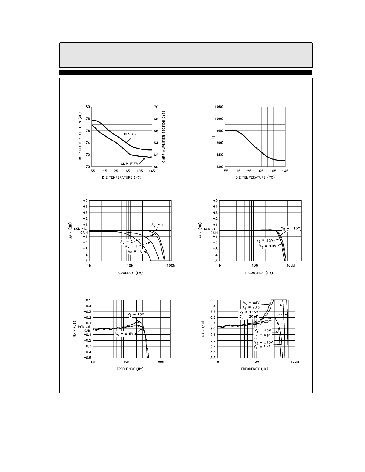
Typical Performance Curves
CMRR for Amplifier and
Restore Section
vs Die Temperature
Relative Frequency Response
for Various Gains, R
e
300X
F
Ð Contd.
4089– 8
Transimpedance (ROL)
vs Die Temperature
Frequency Response vs Supply
e
e
2; R
A
V
300
F
4089– 9
Frequency Response Flatness vs Supply
e
e
2; R
A
V
300
F
4089– 10
4089– 12
4089– 11
Frequency Response Flatness for Various
Load and Supply Conditions
e
e
2; R
A
V
300
F
4089– 13
5
Page 6

EL4089C
DC Restored Video Amplifier
Typical Performance Curves
Frequency Response Flatness
vs C
e
2; R
e
300
F
;A
b
IN
V
Ð Contd.
4089– 14
Differential Phase vs DC Input
Offset; A
R
e
e
2; F
O
3.58 MHz;
V
e
150X
L
Differential Gain vs DC Input
Offset; A
R
e
e
2, F
O
3.58 MHz,
V
e
150X
L
4089– 15
8-Pin Plastic DIP
Maximum Power Dissipation
vs Ambient Temperature
4089– 17
4089– 16
8-Lead SO
Maximum Power Dissipation
vs Ambient Temperature
4089– 18
6
Page 7

EL4089C
DC Restored Video Amplifier
Typical Application
The EL4089 can be used to DC-restore a video
waveform (see Fig. 1). The above circuit forces
the cable driving video amplifier’s output to
ground when the HOLD pin is at a logic low.
The ‘‘correction voltage’’ is stored on capacitor
CX1, an external ceramic capacitor. The capacitor value is chosen from the system requirements. The typical input bias current to the video amplifier is 1 mA, so for a 62 ms hold time, and
a 0.01 mF capacitor, the output voltage drift is
6.2 mV in one line.
The S/H amplifier can provide a typical current
of 300 mA to charge capacitor CX1, so with a
1.2 ms sampling time, the output can be corrected
by 36 mV in each line.
Using a smaller value of CX1 increases both the
voltage that can be corrected, and the drift while
being held, likewise, using a larger value of CX1,
reduces the voltages.
The RX1 resistor is in the circuit purely to simulate some external source impedance, and is not
needed as a real component. Likewise for RX2.
The 75X back terminating resistor RXT is recommended when driving 75X cables.
The board layout should have a ground plane underneath the EL4089, with the ground plane cut
away from the vicinity of the V
This helps to minimize the stray capacitance on
pin 1.
Power supply bypassing is important, and a
0.1 mF ceramic capacitor, from each power pin to
ground, placed very close to the power pins, together with a 4.7 mF tantalum bead capacitor, is
recommended.
When both digital and Analog grounds are on the
same board, the EL4089 should be on the Analog
ground. The digital ground can be connected to
the Analog ground through a 100X – 300X resistor, near the EL4089. This allows the digital signal a return path, while preventing the digital
noise from corrupting the analog ground.
IN
b
pin, (pin 1).
Figure 1
7
4089– 19
Page 8

EL4089C
DC Restored Video Amplifier
EL4089CJanuary 1996 Rev B
Table of Charge Storage Capacitor vs Droop Charging Rates
Cap Value Droop in 60 ms Charge in 1.2 ms Charge in 4 ms
nF mV mV mV
10 6 36 120
33 1.8 11 36
100 0.6 3.6 12
Basic formulae are:
V (droop)
and V (charge)
eIba
* (Line timebSample time) / Capacitor
e
I
* Sample time / Capacitor
OUT
For best results the source impedance should be
kept low, using a buffer for example.
pled during active video. Typically the sample is
made during the back porch period of horizontal
blanking. For this reason color composite signals,
Because the S/H effectively shorts the input signal during Sample, the input should not be sam-
which have color burst on the back porch, can
not be passed. See EL2090 or EL4093 for this ap-
plication.
General Disclaimer
Specifications contained in this data sheet are in effect as of the publication date shown. Elantec, Inc. reserves the right to make changes
in the circuitry or specifications contained herein at any time without notice. Elantec, Inc. assumes no responsibility for the use of any
circuits described herein and makes no representations that they are free from patent infringement.
WARNING Ð Life Support Policy
Elantec, Inc. products are not authorized for and should not be
used within Life Support Systems without the specific written
consent of Elantec, Inc. Life Support systems are equipment in-
Elantec, Inc.
1996 Tarob Court
Milpitas, CA 95035
Telephone: (408) 945-1323
(800) 333-6314
Fax: (408) 945-9305
European Office: 44-71-482-4596
tended to support or sustain life and whose failure to perform
when properly used in accordance with instructions provided can
be reasonably expected to result in significant personal injury or
death. Users contemplating application of Elantec, Inc. products
in Life Support Systems are requested to contact Elantec, Inc.
factory headquarters to establish suitable terms & conditions for
these applications. Elantec, Inc.’s warranty is limited to replace-
ment of defective components and does not cover injury to per-
sons or property or other consequential damages.
Printed in U.S.A.8
 Loading...