

Page 1
HMOS2 SINGLE CHIP SEMI-GRAPHIC
.
SINGLE CHIP LOW-COST COLOR CRT
CONTROLLER
.
TV STANDARDCOMPATIBLE (50Hz or 60Hz)
.
2 SCREENFORMATS :
- 25 (or 21) ROWS OF 40CHARACTERS
- 25 (or 21) ROWS OF 80CHARACTERS
.
ON-CHIP 128 ALPHANUMERIC AND 128
SEMI-GRAPHIC CHARACTER GENERATOR
TWO STANDARD OPTIONS AVAILABLEFOR
ALPHANUMERIC SETS (EF9345-R003IS NO
MOREAVAILABLE)
.
EASY EXTENSION OF USER DEFINED ALPHANUMERIC OR SEMI-GRAPHICSETS
(> 1 K CHARACTERS)
.
40CHARACTERS/ROWATTRIBUTES : FOREGROUNDANDBACKGROUNDCOLOR,DOUBLE HEIGHT, DOUBLE WIDTH, BLINKING,
REVERSE, UNDERLINING, CONCEAL, INSERT, ACCENTUATION OF LOWER CASE
CHARACTERS
.
80 CHARACTERS/ROW ATTRIBUTES : UNDERLINING, BLINKING, REVERSE, COLOR
SELECT
.
PROGRAMMABLE ROLL-UP, ROLL-DOWN
ANDCURSOR DISPLAY
.
ON-CHIPR, G, B, I VIDEOSHIFTREGISTERS
.
EASY SYNCHRONIZATION WITH EXTERNAL VIDEO-SOURCE : ON-CHIP PHASE
COMPARATOR
.
ADDRESS/DATA MULTIPLEXED BUS DIRECTLYCOMPATIBLE WITH STANDARD MICROCOMPUTERS SUCH AS 6801, 6301,
8048,8051, ST9
.
ADDRESSING SPACE : 16K x 8 OF GENERALPURPOSE PRIVATEMEMORY
.
EASY OF USE OF ANY LOW-COST MEMORYCOMPONENTS: ROM, SRAM,DRAM
DESCRIPTION
The EF9345,new advancedcolor CRT controller,
in conjunctionwith an additional standardmemory
packageallowfull implementation of the complete
displaycontrolunit of a color or monochromelowcost termainl, thus significantly reducing IC cost
and PCB space.
DISPLAY PROCESSOR
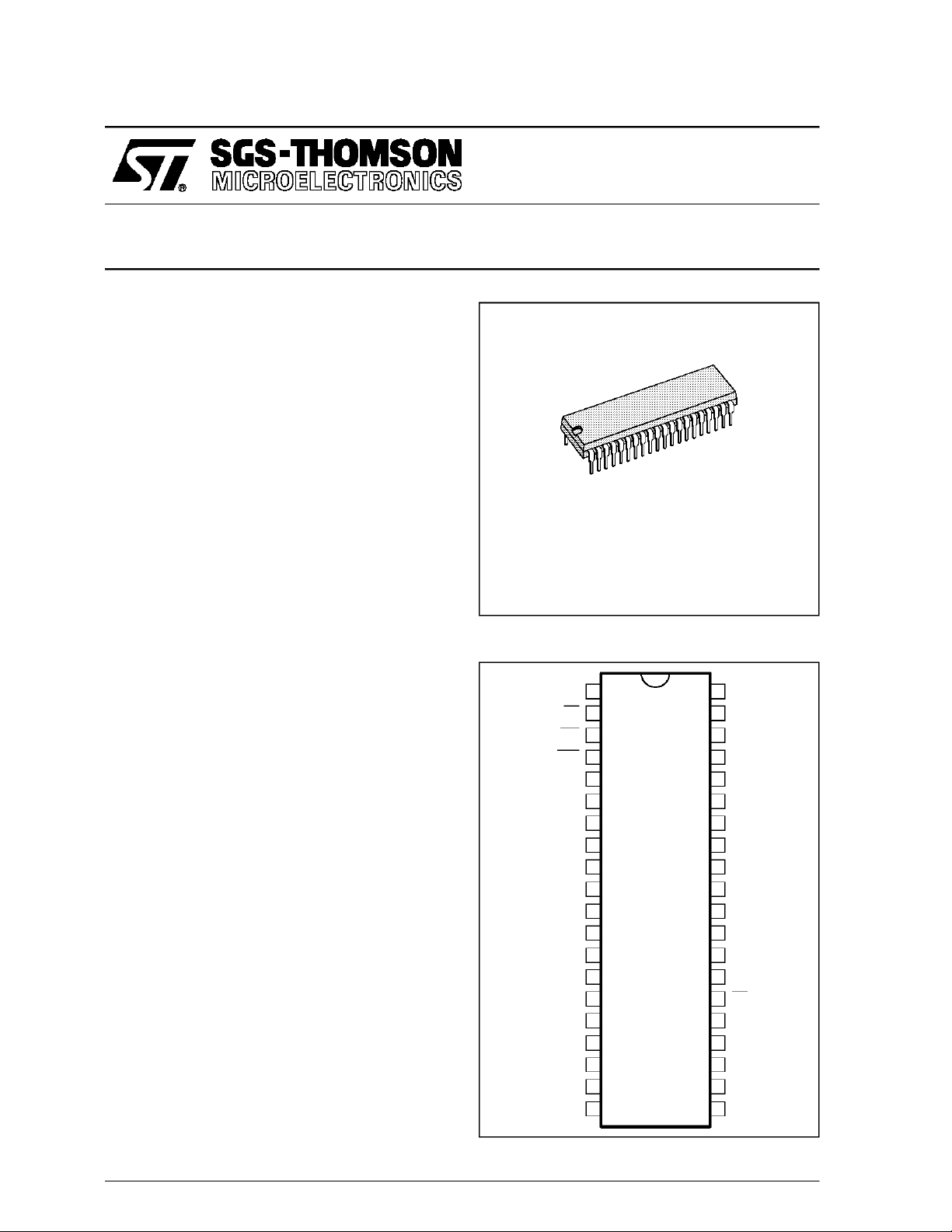
(Plastic Package)
ORDER CODE : EF9345P
PIN CONNECTIONS
V
ASM
HVS/HS
PC/VS
CLK
SYNC IN
R/W
AD0
AD1
AD2
V
OE
WE
HP
AS
DS
1
SS
2
3
4
5
6
B
7
G
8
R
9
I
10
11
12
13
14
15
16
17
18
19
20
CC
DIP40
EF9345
40
ADM0
39
ADM1
38
ADM2
37
ADM3
36
ADM4
35
ADM5
34
ADM6
33
ADM7
32
AM8
31
AM9
30
AM10
29
AM11
28
AM12
27
AM13
26
CS
25
AD7
24
AD6
23
AD5
22
AD4
21
AD3
9345-01.EPS
March 1995
1/38
Page 2
EF9345
PIN DESCRIPTION(All the input/outputpins are TTLcompatible)
Name
MICROPROCESSORINTERFACE
AD(0:7) I/O
AS I 14
DS I 15 Data Strobe
R/W I 16 Read/Write
CS I 26 Chip Select The EF9345 is selected when this inputis strobed low by AS.
MEMORY INTERFACE
ADM(0:7) I/O 40-43
AM(8:13) O 32-27
OE O 2 Output Enable When low, this output selects the memory data output buffers.
WE O 3 Write Enable
ASM O 4
OTHER PINS
CLK I 12 Clock Input External TTL clock Input (nominal value : 12MHz, duty cycle : 50%).
V
SS
V
CC
VIDEO INTERFACE
R
G
B
I O 10 Insert
HVS/HS O 5 Sync. Out
PC/VS O 6
SYNC IN I 13 Synchro In
HP O 11 Video Clock This output delivers a 4MHz clock phased with theR, G, B, I signals.
Pin
Type
Pin N° Function Description
17-29
21-25
Multiplexed
Address/Data
Bus
Address
Strobe
These 8 bidirectional pins provide communication with the
microprocessor system bus.
The falling edge of this control signal latches the address on the
AD(0:7) lines,the state of the Data Strobe (DS) and Chip Select (CS)
into the chip.
When this input is strobed high by AS, the output buffers are selected
while DS is low fora read cycle (R/W = 1).
In write cycle, data present on AD(0:7) lines are strobed by R/W low
(see timing diagram 2).
When this input is strobed low by AS, R/W gives the direction of data
transfer on AD(0:7) bus. DS high strobes the data to be written during
a write cycle (R/W = 0) orenables the output buffers during a read
cycle (R/W = 1). (see timing diagram 1).
This input determines whether the Internal registers get written or
read. A write is active low (”O”).
Multiplexed
Address/Data
Lower 8 bits of memory address appear on the bus when ASM is
high. It then becomes the data bus when ASMis low.
Bus
Memory
These 6 pins provide the highorder bits of the memory address.
Address Bus
This output determines whether the memory gets read or written. A
write is activelow (”0”).
Memory
Address
This signal cycles continuously. Address can be latched on its falling
edge.
Strobe
S 1 Power Supply Ground.
S 20 Power Supply +5V
O
O
O
7
8
9
Red
Green
Blue
These outputs deliver the videosignal. They are low during the
vertical and horizontal blanking intervals.
This active high output allows to insert R : G: B : in an external video
signal forcaptioning purposes, for example. It can also be used as a
general purpose attribute or color.
This output delivers either the composite synchro (bit TGS
horizontal synchro signal (bit TGS
Phase
Comparator /
When TGS
When TGS
Vertical Sync
This input allows vertical and/or horizontal synchronizing the EF9345
on an externalsignal. Itmust be grounded if not used.
=0)
4
= 1, this signal is the phase comparator output.
4
= 0, this output delivers the vertical synchro signal.
4
4
= 1) or the
9345-01.TBL
2/38
Page 3
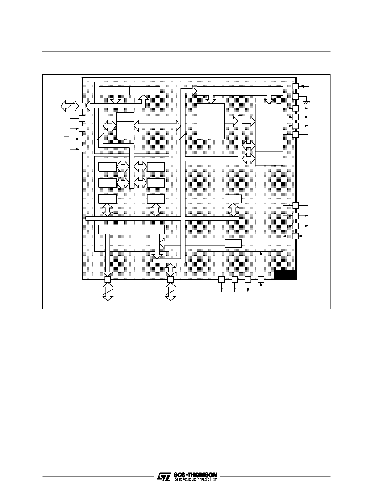
BLOCK DIAGRAM
EF9345
AD(0:7)
AS
STA CMD
8
14
15DS
16R/W
16CS
MPU ACCESS
8
R3R4
R3R6
R3ROR
TRANSCODER
ADDRESS UNIT
R1
R2
R3
R3R5
R3R7
R3DOR
8
DATA BUS
ROW BUFFER 120 x 8
ROM
R3TSG
R3RFSH
ATTRIBUTE
LOGIC
MAT
PAT
TIMING
GENERATOR
+5V
R
9
G
8
B
7
I
10
11
HP
HVS/HS
5
5
PC/VS
6
6
13
SYNC.IN
AM(8:13)
R3
3
2
4
6
ADM(0:7)
8
WE
OE
ASM
CLK
EF9345
12
9345-02.EPS
3/38
Page 4

EF9345
ABSOLUTEMAXIMUM RATINGS
Symbol Parameter Value Unit
* Supply Voltage -0.3, 7.0 V
V
CC
* Input Voltage -0.3, 7.0 V
V
in
T
A
T
stg
P
Dm
* With respect to Vss.
Stresses above those hereby listed may cause permanent damage tothe device. The ratings are stress ones only and functional operation of
the device atthese or any conditionsbeyond thoseindicatedinthe operational sectionsof this specificationis notimplied. Exposure tomaximum
rating conditionsfor extendedperiods may affect reliability. StandardMOS circuits handlingprocedure should be used toavoid possibledamage
to the device.
Operating Temperature 0, +70
Storage Temperature -55, +150
Maximum Power Dissipation 0.75 W
ELECTRICAL CHARACTERISTICS
=5.0V ±5%, VSS=0V,TA= 0 to +70°C,unless otherwisespecified.
V
CC
Symbol Parameter Min. Typ. Max. Unit
V
CC
V
IL
V
IH
I
IN
V
OH
V
OL
P
D
C
IN
I
TSI
Supply Voltage 4.75 5 5.25 V
Input Low Voltage -0.3 0.8 V
Input HighVoltage : CLK
Other Inputs
2.2
2
V
CC
V
CC
Input Leakage Current 10 µ
Output HighVoltage (I
Output Low Voltage : I
= -500µA)
load
= 4mA ; AD(0:7), ADM(0:7), AM(8:13)
load
= 1mA ; Other Outputs
I
load
2.4 V
0.4
0.4
Power Dissipation 250 mW
Input Capacitance 15 pF
Three State (Off State) Input Current 10 µ
o
C
o
C
V
A
V
A
9345-02.TBL
9345-03.TBL
4/38
Page 5

EF9345
MEMORYINTERFACE
=5.0V ±5%, TA=0 to + 70°C
V
CC
Clock : f
ReferenceLevels: V
Symbol Ident. N° Parameter Min. Typ. Max. Unit
t
ELEL
t
EHEL
t
ELDV
t
t
AVEL
t
ELAX
t
CLAZ
t
GHDX
t
t
GLDV
t
QVWL
t
WHQX
t
WLWH
= 12MHz ; DutyCycle 40 to 60% ; tr,tf< 5ns
in
= 0.8Vand VIH=2V,VOL= 0.4V and VOH=2.4V
IL
1 Memory Cycle Time 500 ns
t
D
2 Output Delay Time from CLK Rising Edge (ASM, OE, WE) 60 ns
3 ASM High Pule Width 120 ns
4 Memory Access Time from ASM Low 290 ns
DA
5 Output Delay Time from CLK Rising Edge (ADM(0:7), AM(8:13)) 80 ns
6 Address Setup Time to ASM 30 ns
7 Address Hold Time from ASM 55 ns
8 Address Off Time 80 ns
9 Memory Hold Time 10 ns
OZ
10 Data Off Time from OE 60 ns
11 Memory OE Access Time 150 ns
12 Data Setup Time (Write Cycle) 30 ns
13 Data Hold Time (WriteCycle) 30 ns
14 WE Pulse Width 110 ns
9345-04.TBL
Figure 1 : TestLoad Table 1
V
DD
Symbol
C 100pF 50pF
R
Test
Point
R
L
C
L
R
MMD7000
or equivalent
R
9345-03.EPS
Figure 2 : Memory Interface Timing Diagram
1
2
D
2
11
3
56 7
IN
9
10
CLK
ASM
ADM (0:7)
AM (8:14)
OE
WE
T
2
56 7
READ ADDRESS WRITE ADDRESS
4
8
2
AM(8:13)
ADM(0:7)
AD(0:7)
L
1kΩ 3.3kΩ
4.7kΩ 4.7kΩ
5
D
OUT
22
12 13
14
Other
Outputs
9345-05.TBL
9345-04.EPS
5/38
Page 6

EF9345
MICROPROCESSORINTERFACE
EF9345 is motel compatible. It automaticallyselects the processortype by using AS input latch to
state of the DS input.
No external logic is needed to adapt bus control
signals frommost of the common multiplexed bus
microprocessors.
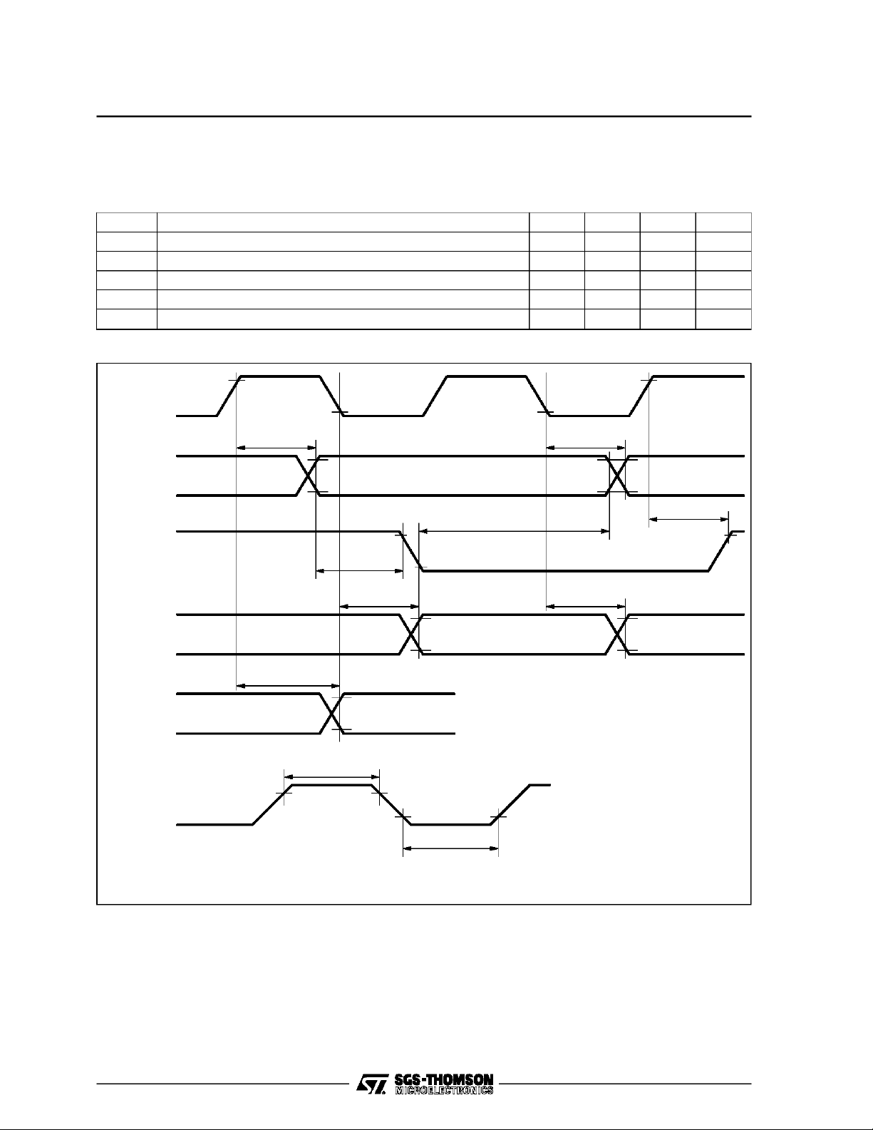
MICROPROCESSORINTERFACE TIMING AD(0:7), AS, DS, R/W, CS
V
= 5.0V ±5%,TA= 0 to + 70°C, CL=100pF on AD(0:7)
CC
ReferenceLevels : V
Symbol Ident. N° Parameter Min. Typ. Max. Unit
t
CYC
t
ASD
t
ASED
t
PWEH
t
PWASH
t
RWS
t
RWH
t
ASL
t
AHL
t
DSW
t
DHW
t
DDR
t
DHR
t
ACC
1 Memory Cycle Time 400 ns
2
3
4 Write Pulse Width 200 ns
5 AS Pulse Width 100 ns
6 R/W to DS Setup Time (Timing 1) 100 ns
7 R/W to DS Hold Time (Timing 1) 10 ns
8 Address and CS Setup Time 20 ns
9 Address and CS Hold Time 20 ns
10 Data Setup Time (Write Cycle) 100 ns
11 Data Hold Time (Write Cycle) 10 ns
12 Data Access Time from DS (Read Cycle) 150 ns
13 DS Inactive to High Impedance State Time (Read Cycle) 10 80 ns
14 Address to Data Valid Access Time 300 ns
=0.8V and VIH=2V on All Inputs ; VOL= 0.4V andVOHonall Outputs.
IL
DS Low to AS High (Timing 1)
DS High or R/W High to AS High (Timing 2)
AS Low to High (Timing 1)
AS Low to DS Low or R/W Low (Timing 2)
EF9345 6801 INTEL Family
Timing 1 Timing 2
AS AS ALE
DS
DS, E, φ 2
RD
R/W R/W WR
30 ns
30 ns
9345-06.TBL
Figure 3 : MicroprocessorInterfaceTiming Diagram1 (6801 Type)
1
3
2
5
6
8
ADDRESS
8
ADDRESS
9
9
12
14
6/38
DS
ASM
R/W
CS
WRITECYCLE
AD (0:7)
READ CYCLE
AD (0:7)
10
INPUT DATA
OUTPUT
DATA
2
7
11
13
9345-05.EPS
Page 7

Figure 4 : MicroprocessorInterfaceTiming Diagram2 (INTEL Type) - ReadCycle
1
EF9345
ALE
(Pin AS)
23
5
RD
(Pin DS)
WR
(Pin R/W)
2
12
CS
AD(0:7)
8
9
ADDRESS
14
13
D
OUT
Figure 5 : MicroprocessorInterfaceTiming Diagram2 (INTEL Type) - Write Cycle
1
ALE
(Pin AS)
RD
(Pin DS)
2
2
5
3
4
9345-06.EPS
WR
(Pin R/W)
CS
AD(0:7)
89
ADDRESS
10
11
D
IN
9345-07.EPS
7/38
Page 8
EF9345
VIDEO INTERFACE R, G, B, I, HP, HVS/HS, PC/VS
V
= 5.0V ±5%,TA= 0 to + 70°C, CLK Duty Cycle = 50%, CL=50pF
CC
ReferenceLevels : V
Symbol Parameter Min. Typ. Max. Unit
t
t
HO
t
t
PWCH
t
PWCL
Setup Time R, G, B, I to HP 10 ns
SU
Hold Time R, G, B, I fromHP 50 ns
Output Delay from CLK Edge 60 ns
D
CLK High Pulse Width 30 ns
CLK Low Pulse Width 30 ns
Figure6
CLK
=0.8V and VIH=2.2V on CLK Inputs.VOL=0.4V and VOH= 2.4V on all Outputs.
IL
9345-07.TBL
R, G, B, I,
40 char/row
HP
R, G, B, I,
80 char/row
HVS/HS
PC/VS
INPUT CLK
CLK
t
D
t
HO
t
SU
t
D
t
D
t
PWCH
t
PWCL
t
D
t
D
t
D
8/38
9345-08.EPS
Page 9
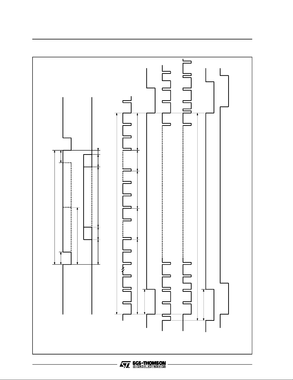
Figure 7 : Vertical and Horizontal SynchronizationOutputs (CLK = 12MHz)
Blanking 3 Lines
2.04µs
4.5µs4.5µs
Margin
18 Lines
EF9345
Bulk
40µs6µs2µs
40µs6µs6µs
=0)
=1)
0
312 lines (TGS
0
362 lines (TGS
64µs
6µs40 char/row
Margin Margin H BlankingH Blanking
32µs
Odd frame 1/2 pulse Even frame 1/2 pulse
10µs
9.96µs
=0)
0
312.5 lines (TGS
=1)
0
362.5 lines (TGS
80 char/row
Blanking 25 Lines Margin 16 Lines Page 250 Lines
2 lines
2.5 lines
=0)
4
HVS
OHVOL
V
=0
= 1 25 Lines 10 Lines 210 Lines 14 Lines 3Lines
0
R, G, B, I
=1)
0
4
TGS
TGS
=0)
4
=1)
4
HORIZONTAL SYNCHRO
VERTICAL SYNCHRO
NON INTERLACED
HVS (TGS
VS (TGS
INTERLACED
Even Frame
HVS (TGS
Odd Frame
Even Frame
VS (TGS
Odd Frame
9345-09.EPS
9/38
Page 10

EF9345
FUNCTIONAL DESCRIPTION
The EF9345is a low cost, semigraphic,CRT controller.
It is optimizedfor use witha lowcost, monochrome
or color TV type CRT (64ms per line, 50 or 60Hz
refresh frequency).
The EF9345 displays up to 25 rows of 40 characters or 25 rows of 80 characters.
The on-chip character generator provides a 128
standard, 5 x 7, character set and standard semigraphic sets.
More usedefinable(8 x 10) alphanumericor semigraphicsets may bemappedin the16K x8 private
memory addressingspace.
These user definable sets are available only in 40
charactersper row format.
MicroprocessorInterface
The EF9345 provides an 8-bit, adress/data multiplexed microprocessorinterface.
It is directly compatible with popular (6801, 8048,
8051, 8035,...) microprocessors.
40 Charactersper Row : Character Code
Formatsand Attributes
Once the 40 characters per row format has been
selected, one character code format out of three
must be chosen :
- 24-bit fixed format :
All the attributesare providedin parallel.
- 8/24-bit compressedformat :
All the attributesare latched.
- 16-bit fixed format :
Some parallel attributes,other are latched.
Characterattributesprovided :
- Backgroundand foregroundcolor (3 bits each),
- Doubleheight, double width,
- Blinking,
- Reverse,
- Underlining,
- Conceal,
- Insert,
- Accentuationof lower casecharacters,
- 3 x 100 user definable character generator in
memory,
- 8 x 100semi-graphicquadrichromecharacters.
Registers
The microprocessordirectly accesses8 registers:
- R0 : Command/status register.
- R1, R2, R3 : Data registers.
- R4, R5, R6, R7 : Each of these register pairs
pointsinto the private memory.
Through these registers, the microprocessorindirectly accesses the private memory and 5 more
registers :
- ROR, DOR : Base address of displayed page
memoryand usedexternalcharactergenerators.
- PAT, MAT, TGS : Usedto select the page attributes and format, and to program thetiming generatoroption.
Private Memory
The usermay partitionthe 16Kx 8 private memory
addressingspace between :
- Page ofcharacter codes(2 K x 8 or 3 K x 8),
- Externalcharacter generators,
- Generalpurposeuser area.
Many types of memory componentsare suitable :
- ROM, DRAMor SRAM,
- 2 K x 8, 8 K x 8, 16 K x 4 organizations,
- Modest 500ns cycletime and 250nsaccess time
is required.
80 Charactersper Row Format : Character
Code Format and Attributes
Two character code formats are provided :
- Long (12 bits)with 4 parallel attributes:
• Blinking,
• Underlining,
• Reverse,
• Color select.
- Short (8 bits) : no attributes.
Timing Generator
The whole timing is derived from a 12MHz main
clock input.
The RGB outputs are shifted at 8MHz for the 40
character/row format and at 12MHz for the 80
character/row.
Besides,the user mayselect :
- 50Hz or 60Hzvertical sync. frequency,
- Interlacedor not,
- Separated or composite vertical and horizontal
sync.ouputs.
Furthermore,a compositesync.inputallows,when
it is required :
- An on-chip vertical resynchronization,
- An on-chip crude horizontalresynchronization,
- An off-chip high performance horizontal resynchronization by use of a simple external VCXO
controlledby theon-chip phase comparator.
10/38
Page 11

MEMORYORGANIZATION
Logical And PhysicalAddressing
The physical16-Kbyteaddressingspaceis logicaly
partitioned by EF9345 into 40-byte buffers (Figure 8). Moreprecisely,a logicaladdressisgiven by
an X, Y,Z triplet where :
- X = (0 to 39) points to a byte inside a buffer,
- Y = (0, 1 ; 8 to 31) points to a buffer inside a
1 Kbyte blocks,
- Z = (0 to 15) points to a block.
Obviously, 1 K = 2
10
= 1024 cannot be exactly
divided by 40. Consequently, any block holds 25
full buffersand a24-byte remainder.Provided that
the physicalmemory is a multiple of 2 Kbytes, the
remainders are paired in sucha way as to make
available:
- A full buffer (Y = 1) in each evenblock,
- A partial buffer (Y = 1 ; X = 32 to 39)in each odd
block.
Figure 8 : Memory Row Buffer
EF9345
Pointers
EachX, Y and Z componentof alogical address is
binaryencodedand packed in two 8-bitsregisters.
Sucha registerpair is a pointer (Figure9). EF9345
containstwo pointers :
- R4, R5 : auxiliary pointer,
- R6, R7 : main pointer.
R5 and R7 have the same format. Each one holds
an X componentand the two LSB’sof a Z component. This packing induces a partitioning of Z in 4
districts of 4 blockseach.
R5, R7 points to a block number in a district. R4
and R6 have a slightlydifferent format : Each one
holds a Y component and the LSB of the district
number. But R6 holds bothdistrictMSB
Figure 11 gives the logical to physical address
transcodingscheme performed onchip.
Figure9 : PointerAuto Incrementation
X
839
32 32
DISTRICT
0
1
8
31
00
1
8
Y
31
0
1
8
31
0
1
8
31
0
9
DISTRICT
DISTRICT
120-BYTE ROW BUFFER 80-BYTE ROW BUFFER
- Row buffers lay indide a district
Notes :
- At two or threesuccessiveblock addresses (modulo 4)
- First block address is even
BLOCK0
(1Kbyte)
BLOCK1
BLOCK2
BLOCK3
839
X
Y
39 1
9345-10.EPS
Y = (0, 1 ; 8 to 31)
d1d’1d043210R6
X=0to39
b0b1543210R7
Y’ = (0, 1 ; 8 to 31)
__
b’0b’1543210R5
X incrementation
d’043210R4
X’ = 0 to 39
0
2=0
4=0
6=0
0
XYB
Modulo40
89
31
2
Y incrementation
1
3=1
5=1
7=1
Modulo24
MAIN
POINTER
AUXILIARY
POINTER
Z = (0 to 15)
3210
DB
1
10
0
3
Z incrementation/
decrementation
Modulo4 on the
blocknumber only
2
9345-11.EPS
11/38
Page 12
EF9345
Data Structure in Memory
A page is a data structure displayable on the
screen up to 25 rows of characters. According to
the charactercode format, eachrow on the screen
is associatedwith 2 (or 3)40-bytebuffers. This set
of 2 (or 3) buffers constitutes a row buffer (Figure 8). Thebuffers belongingto arow buffer must
meet the followingrequirements :
- They have the same Y address,
- They have the same district number,
- They lie at 2 (or 3) successive (modulo 4) block
addressesin their common district.
Consequently, a row buffer is defined by its first
buffer address andits format.
A pageis a set of successiverow buffers :
- With thesame format,
- With thesame districtnumber,
- With the same block address of first buffer. This
blockaddress must be even,
- Lyingat successive(modulo 24) Y addresses.
Figure 10 : MemoryCycle Allocation
40µs24µs
Consequently, a page should not cross a district
boundary.General purpose memory area may be
used but should respect the buffer of row buffer
structure. See Figure 9 for pointer incrementation
implied by these data structures.
MemoryTime Sharing (See Figure10)
Thememoryinterfaceprovidesa 500ns cycletime.
Thatis to say a 2 Mbyte/smemory bandwith. This
bandwithis shared between :
- Reading a row buffer from memory to load the
internalrowbuffer(upto120bytesonceeachrow),
- Readinguser definedcharactersslicesfrom memory (1 byte each µs),
- Indirectmicroprocessor read or write operation,
- Refreshcycles to allowDRAM use, withno overhead.
A fixed allocation schemeimplements the sharing.
During these lines, no microprocessor access is
provided for 104µs ; this hold too when no user
definedcharacter slices are addressed.
312/362
250/210
SCAN
ACTIVE
LINES
SCAN
LINES
INACTIVE LINE
LAST ROW LINE
FIRST ROW LINE
OTHER ROW LINE
Notes : 1. Dummy cycles are read cycles at dummyaddresses.
2. RFSH cycles are read cycles performed by an 8-bit auto-incrementing counter. Low order address byte ADM(0:7) cycles
through its 256 statesin less than 1ms.
3.
The microprocessor may indirectly access the memory once every µs, except during the first and the last line of a row, when
the internalbuffer must be reloaded.
ACTIVE
DISPLAY
TIME
DUM
µP
UDS
LD
UDS
LD
UDS
µP
1µs
40µs24µs
RFSH
LD
RFSH
RFSH
µP
LD
µP
µP
1µs
ONE ROW = 10 SCAN LINES
MEMORY CYCLE
DUM : dummy cycle
µP : indirect access to memory
RFSH : refresh cycle
UDS :slice read cycle
LD : read cycle to load the internal row buffer
Figure 11 : Logicalto PhysicalAddress TranscodingPerformed On-chip
Z (0 to 15) Y (0, 1 ; 8 to 31) X (0 to 39)
DB
LOGICAL
ADDRESS
3210 43210 43210
TRANSCODING
5
9345-12.EPS
12/38
PHYSICAL
ADDRESS
131211 109876543 210
9345-13.EPS
Page 13

Table 2
EF9345
X and Y
Condition
Y≥8
Y<8
Y0 = 1
X5 = 0 b0 Y4 Y3 Y2 Y1 Y0 X4 X3
X5 = 1 b0 0 0 Y2 Y1 Y0 Y4 Y3
Y0 = 0 b0 0 0 X5 X4 X3 0 0
b0 = 0 X3 0 0 I X5 X4 0 0
b0 = 1 I 0 0 I X5 X4 0 0
109876543
SCREEN FORMATAND ATTRIBUTES
The screenformat and attributes are programmed
through 5 indirectly accessible registers : ROR,
TGS, PAT, MAT and DOR. IND command allows
accessing these registers. TGS is also used to
select the timing generator options (see Table 3).
Row and Character Code Format
; TGS
PAT
7
(6:7)
Two row formatsand5 charactercode formatsare
available but cannot be mixed in a given screen.
DOR register interpretation is completely row format dependentandis discussedin thecorrespondnig 40 char/row and 80 char/row section.
Physical Address AM(3:10)
BULK : TGS0; PAT
(1:2)
; MAT
7
It is displayed after the service row for 200 or 240
TV lines according to TGS
. Each row buffer is
0
usually displayed for 10 TV lines. However,
=1 doublesthis figure.Theneverycharacter
MAT
7
appearsin doubleheight(doubleheightcharacters
are quadrupled).
=0 and/orPAT2=0 disablesrespectivelythe
PAT
1
upper120linesand/orthe lower80/120lines ofthe
bulk.
When disabled, the corresponding TV lines are
displayedas a marginextension.
ScreenPartition - Page Pointer ROR
(See Table 3)
The screenis partitionedinto 3 areas :
- The margin,
- The servicerow,
- The bulk of remainingrows.
MAT
value I
declares the color of the margin and the
(0:3)
of its insert attribute.
M
RORregisterpointstothepagetobedisplayedand
gives the 3 MSB’s of the Z address : Z
0
=0
implicitly ; the page block address must be even.
YOR gives the first row buffers to be displayedat
the topof the bulk area. The next row buffers to be
displayedare fetchedsequentiallyby incrementing
the Y address (modulo 24). This address never
gets out of the originblock.Incrementationof YOR
by the microprocessoryields a rollup.
Service Row : TGS
- PAT
5
0
The servicerow is displayed for 10 TV lines ontop
of the screen and does not roll. Following TGS
5
,it
is fetchedfrom the origin block at eitherY = 0 or Y
= 1.The Y = 1is a partialrow buffer.It can beused
only with variable 40 char./row and an 8 byte
attribute file. The service row may be disabled by
=0 ; it isthe displayedasa marginextension.
PAT
0
CursorMAT
(4:6)
To be displayedwith the cursor attributes,a charactermust be pointedby the mainpointer(R6, R7)
and MAT6 must be set. The cursor attributes are
given by MAT
(4:5)
:
- Complementation : theR, G and B of eachpixel
is logicallynegated.
R, G, B → R,G, B
- Underline: theunderlineattributeof thischaracter is negated.
- Flash : the character is periodically displayed
with, then without, its cursor attributes (50% /
50% ; ≈1Hz).
Flash Enable (PAT
) - Conceal Enable (PAT3)
6
Any character flashing attribute is a ”don’t care”
whenPAT
=0. WhenPAT6=1, acharacterflashes
6
if its flashing attribute is set. It is then periodically
displayedas a space(50% / 50% ; 0.5Hz).
is a ”don’t care” for80 char./row formats.
PAT
3
Whenany 40 char./row format is in use :
-IfPAT
=0 the concealattributeof anycharacter
3
is a don’t care
-IfPAT
=1,the concealattribute of eachcharac-
3
ter is interpreted: aconcealedcharacterappears
as aspace on the screen.
13/38
Page 14

EF9345
Insert Modes : PAT
(4:5)
During retrace, margin and extended marginperiods, the I outputpin deliversthe value of the insert
margin attribute.
I=I
= MAT
M
4
During active line period, the I output state is controlled by the Insert Mode and i, the insertattribute
of each character. The I output pin may have
severaluses (see Figure12) :
- As a margin/activearea signal in the active area
markmode.
- As acharacter per charactermarkersignalin the
charactermark mode.
- As a video mixing signal in the two remaining
modes,provided that the EF9345has been vertically and horizontally synchronizedwith an external video source : the Ipin allows mixingRGB
outputs (I = 1) and the external video signal
(I = 0). This mixing can be achieve by switching
or Oring. It may occurfor the complete character
window(Boxing Mode)or only forthe foreground
pixels(Inlay Mode).
Table 3 : Video OutputsDuring Active Periods
Char. Level Outputs
Insert Mode
Active Area Mark – 1 X
Character Mark
Boxing
Inlay
Notes : 1. Pixel type :
– : Dont’t care.
FOREGRND= Aforeground pixel is :
- Any pixel of a quadrichromecha racter,
- A pixel of a bichromecharacter generated from a ”1” in the
charactergenerator cell.
2. RGB outputs :
X : Not affected.
BLACK : Forced to low level.
i Pixels
0–0X
1–1X
0 – 0 BLACK
1–1X
0 – 0 BLACK
1 BACKGND 0 BLACK
FOREGND 1 X
(1)
I
R, G, B
(2)
Timing GeneratorOptions : TGS(0:4)
TGS
selectthe number of lines per frame :
(0:1)
TGS
0 0 312
0 1 262
1 0 312.5
1 1 262.5
TGS
1
LINES
0
NON INTERLACED
INTERLACED
The compositeincoming SYNC IN signal is separated into 2 internals signals :
- VerticalSynchronizationIn (VSI),
- Horizontal SynchronizationIn (HSI).
enable VSI to reset the internal line count.
TGS
3
SYNC IN input is sampled at the beginningof the
activeareaof each line. When the sample transits
from1 to 0, the line count is reset at the end of the
currentline.
TGS
enables HSI to control an internal digital
2
phase lock loop. HSI and on-chip generated HS
Out are considered as in phase if their leading
edgesmatch at ±1 clockperiod.
When they are out of phase, the line period is
lengthenedby 1 clockperiod (≈80ns).
controlsthe SYNC OUT pins configuration :
TGS
4
TGS4 HVS / HS PC / VS
1 Composite Sync PC
0 H Sync Out V Sync Out
PC is the output of the on-chipphase comparator.
An external VCXO allows a smoother horizontal
phaselock than the internal scheme.
Figure12
SYNC IN
HVS/HS
CLK
DQ
HS
VS
÷6
DQ
PC
9345-14.EPS
14/38
Page 15

Table 3 : ScreenFormat
EF9345
MARGIN
YOR
+23
BULK
Service
Row
YOR
SERVICEROW
Y ORIGIN
Y ORIGIN + 1
YOR+1
YOR+2
039
MEMORY
BLOCKORIGIN
(even)
0
1
TGS
8
YOR
YOR +1
31
76 543210
Z3Z1Z
2
76543210
5
ROR (r = 7)
Origin row address
YOR = (8 to 31)
Blockorigin (even)
Servicerow select
(Y = 1/0)
Char Code TGS7TGS
40 CHARLONG
40 CHARVAR
40 CHARSHORT
80 CHARLONG
80 CHARSHORT
PAT
0
0
1
0
0
7
0
0
0
1
1
Insert Mode PAT5PAT
INLAY
BOXING
CHARACTERMARK
ACTIVEAREA MARK
CursorDisplaymode
FIXEDCOMPLEMENTED
FLASHCOMPLEMENTED
FIXEDUNDERLINED
FLASHUNDERLINED
0
0
1
1
MAT5MAT
0
1
0
1
Note : PROGRAMMING BIT VALUE
1 = True, 0 = False
TGS (r = 1)
525/625lines
6
0
1
0
1
0
Interlaced
Horizontalresync enable
Vertical resync enable
Syncout pins configuration
1 : composite sync
+ phasecomparator
0 : V sync + H sync
76543210
PAT (r = 3)
Servicerow enable
4
0
1
0
1
Upperbulk enable
Lowerbulk enable
Concealenable
Flashenable
76543210
4
0
BMGMR
i
M
M
MAT (r = 2)
0
1
1
Margin color
Margin insert
Cursordisplay enable
Doubleheight
9345-15.EPS
15/38
Page 16

EF9345
40 CHAR/ROW CHARACTER CODES
To display pages in 40 character per row format,
one out of three character code formats must be
selected :
- Fixed long (24bits) code : all parallel attributes.
- Fixed short (16 bits) code : mix of parallel and
latchedattributes.
- Variable(8/24 bits) code : all latchedattributes.
Fixed short and variable codes are translatedinto
fixed longcodes by EF9345duringthe internalrow
buffer loadingprocess.The choiceof thecharacter
code format is obviously a display flexibility/memory size trade off, left upto the user.
Fixed Long Codes
This is the basic 40 char./row code.Each 8 pixels
x 10 lines character window, on the screen is
associatedwith a 3-byte code in memory,namely
the C, B and A bytes (Figure 13). A row on the
screen is associated with a 120 byte row buffer in
memory.
3-BYTE Code Structure
1. C7 is a don’t care. Up to 128 characters may
be addressedin eachset.Eachuser definable
set holds only 100 characters : C byte value
ranges from 00 to 03and 20 to 7F (hexa).
2. B(4:7) give the type and set number of the
character.
3. All the bichrome characters have the same
attributes except that alphanumerics may be
underlined,semi-graphics cannot.Accentuated
alphanumerics allow orthogonal accentuating
ofanyoneofthe32 lowercaseROMcharacters
with any of 8 accents(see Figure 27).
Figure 13 : 40 Char/Row Fixed Long Codes
Bichrome Code
76543210
C BYTE
4. Bichrome and quadrichrome characters use
two differentcoloring schemes.
For bichrome characters, character code byte A
defines a two color set by giving directly two color
values (Figure 14). The negative attribute exchanges the two values. Each bit of slice byte
selectsone colorvalue out of two.
The ”A” byte in a quadrichrome character code
defines an ordered 4 colorset (Figure 15). When
more than 4 bits are set, higher ranking bits are
ignored.Whenless than4bits areset,the colorset
is completed with implicit ”white” value. The slice
byte is shifted 2 bits at once at half the dot fre-
quency(≈4MHz).
Eachbit pairdesignatesonecolorout of the4 color
sets.
Quadrichromecharacters allow displaying up to 4
differentcolors(instead of 2) in any 8x 10 window
at the penalty of an halved horizontalresolution.
By programming theR attributein byte B, one may
choseto keepthe full verticalresolution(1 slice per
line) or to halveit (eachslice is repeatedtwice). In
anycase,itispossibletochangethecolorsetfreely
from window to window and to mix freely all the
charactertypes.So,fairlycomplexpicturesmaybe
displayed at low memory cost.
Handling Long Codes
The KRF command allows an easy X, Y random
access or an X sequential access to/from the microprocessor from/to a memory row buffer (Figure 16).
QuadrichromeCode
76543210
NFB
1
16/38
LmHi
G
R
1
B
1
0
B BYTE
Insert
Double height
Conceal
Double width
Type and set
G
R
0
0
A BYTE
Background color C
Flash (blink)
Foreground color C
Negative (reverse video)
0
1
11
4 COLOR PALETTE
kRi
Insert
Low resolution
Subset index
(low resolution only)
Set number
9345-16.EPS
Page 17

Figure13 (Continued)
EF9345
Type and Set
Number of Character
Code : B(4:7)
7654 C(0:6)
011
10 G
00
0
U
N
128 Standard Mosaïcs
32 Strokes
128 Alphanumerics G
D
E
R
10 G
1G
0 0 100 Alpha UDS
L
I
N
E
Accentuated Lower Case Alpha
0 1 0 100 Semi-Graphic UDS G’
1
1 1 100 Semi-Graphic UDS G’
8 Sets of 100
1XX
Quadrichrome Character
Note : Programming bit value : 1 = True ; 0 = False.
Figure 14 : Coloring with BichromeCharacters
Color Value
R
G
B
0
0
0
0
1
1
1
1
1
0
0
1
1
1
0
0
1
0
0
1
1
1
0
0
Black
Red
Green
Yellow
Blue
Magenta
Cyan
White
CHARACTER
CODE A BYTE
Exchanges values
per Set
N=1
Set
Name
G
10
11
0
Set
Type
SEMI-GR
B
I
Location
ON-CHIP
C
H
ALPHA
20
21
G’
0
10
SEMI-GR.
11
Q
0
to
Q
76543210
NFB
G
1
1
33
Quadrichrome
7
R
1
B
R
O
M
E
EXTERNAL
MEMORY
G
0
R
0
0
Cell
ROM
9345-08.TBL
Foreground
SHIFTED SLICE BYTE
(LSB first)
76543210
01010010
Foreground
color
C
1
33
3
C
0
Background
color
MUX
Pixel color
R, G, B
9345-17.EPS
17/38
Page 18

EF9345
Figure 15 : Coloring with QuadrichromeCharacters
76543210
CHARACTER
CODE A BYTE
01011010
76543210
01 C1C
ORDERED
COLOR VALUES
Black
Red
Green
Yellow
Blue
Magenta
Cyan
White
C
3
COLOR
SET
_
C
_
C
C
_
C
_
C
2
0
1
2
3
Color set
0
3
2
SLICE BYTE SHIFTING :
2 bits at once at half the pixel frequency
Figure 16 : FixedLong Codesin Memory 120 Byte Row Buffer
X
KRF COMMAND
C
R1
B
R2
A
R3
R4
R5
R6
R7
-
-
D, Y
B, X
Y
039
C
B
333
3
D district
number
C1(yellow)
B (even)
B+1
MUX (1 out of 4)
9345-18.EPS
18/38
A
B+2
9345-19.EPS
Page 19

EF9345
Variable Codes
In many cases, successive characters on screen
belong to the same character set and have the
same attributes. Variable codes achieve memory
saving by storing B and A bytes only when it is
required by exploitingthe C7 bit.
C7 = 1 This is a long 3-byte code.
Character set and attribute values are
completelyredefinedby B and A bytes.
C7 = 0 This is a short1-byte code.
Character set and attributes value are
identical to the previous code.
A furthersavingcomesfromthe fact thatanaccentuatedalphabeticcharacteris, moreoftenthan not,
followedbya notaccentuatedalphabeticcharacter.
So, G
escape with return to G
or G21sets are processed as one-shot
20
. For normal operation,
0
variablecodes should obeythe followingrules :
- The first charactercode of any row(X= 0)should
be long.
- A character code may be short when it has the
same attributes as the previous character code
and belongs to thesame set.
Figure 17 : Expansion/CompressionMove
However:
- Any code belonging to G
or G21must be long
20
and must be repeated if the character is double
width,
- A code belonging to G
following a G20or G
0
21
code may be short.
Handlingthe Variable Codes
Duringthe displayprocess, a row of variablecode
should be laid in an 80/120 byte row buffer. The
first buffer holds the C bytes. The second buffer
holds theB, Afileprovidingupto 20longcodesper
row (Figure 18). In the exceptionalcasewhen this
is not enough, the second buffer overflows in the
third one. Every code may then be long. Variable
codescanalmostalwaysachievea memorysaving
overlong fixedcodes and cannever be worse.
The KRV command gives a very easy sequential
accessto/from a row buffer from/to the microprocessor. This command automaticallyupdates the C
byte and B, A filepointers (the last onewhen C7 is
set).
EXP and CMP
COMMANDS
R1
R2
R3
R4
R5
R6
R7
-
-
-
ZW, YW
BF, XF
D, Y
B, X
YW
X
039
B
A
C
Y
BA B + 1 = BF
DW
BW (even)
EXPANDED
CODE
BW + 1
D
B (even)
VARIABLE
CODE
XF
9345-20.EPS
19/38
Page 20

EF9345
Random accessto avariable codeisobviouslynot
as easy. The EXP, KRE and CMP commandsare
designed to facilitate thistask (figure17).
The EXPcommand translatesa full row of variable
codes into a row of expanded codes. Expanded
codes are generallynot displayableby verysimilar
to the long codes.
KRE gives a randomaccessto an expandedcode
and makesit appearas a regularlong code.
The CMP command translates a full row of expanded code into a row of variabble codes and
minimizes the filesize in the process.
These commands use a buffer pair as working
area.
Figure 18 : VariableCodes in memory
X
KRV COMMAND
C
R1
B
R2
A
R3
R4
-
R5
BF, XF
R6
D, Y
R7
B, X
Y
039
BA
D district
number
B (even)
B+1=BF
XF :
file pointer
Fixed Short Codes
These fixed 16 bits codes achieve memory saving
by anotherway.They maybe easierto handlethan
variable codes. The penalty is in lesser display
capabilities:
- Accentuated character sets are no longer available : accentuated characters must be individually providedby the character generators.
- G’11 and quadrichrome sets cannotbe reached.
- Someattributes are latchedand can be changed
only whiledisplaying a space (delimitor code).
The KRGcommandallows aneasyaccessfrom/to
an 80-byterowbufferin memoryto/fromthe microprocessor (Figure 19). Figure 20 gives the fixed
shortto fixedlong translationprocesswhichoccurs
for each row - whileloading the internalrow buffer
before display.
Figure19 : Fixed Short Codesin Memory80
X
KRG COMMAND
A*
R1
B*
R2
W
R3
R4
-
R5
-
R6
D, Y
R7
B, X
Y
039
A*
B*
District
B (even)
B+1
20/38
Overflow
buffer
B+2
9345-21.EPS
9345-22.EPS
Page 21

Figure 20 : FixedShort Code to Fixed Long Code Translation
EF9345
ROM
G0
SET
0
C
F
1
C
N
i
H
m
L
BA
U
FIXED LONG CODEFIXED SHORT CODE
00
0
X
MEMOR
G10
0
0
C
C
F
F
1
1
C
C
0
0
i
i
0
0
m
m
0
0
0
0
001
001
Y
G’0
G’10
Negative
space
0
0
0
C
F
1
C
N
i
H
m
L
U
100
C
C
F
0
1
1
C
C
0
1
i
0
Double width
m
0
00
101 i
:::
m
LHC
0
U
001
Negative
:::
NUX
Latched
attribute
Double height
Backgroundcolor
Foregroundcolor
:
0C1
Underline
Character code
Deliminator
:
DEL
The translation process operates through 3 elementary operations :
, flashing) is directly loaded from short to long code.
0
- Field-to-constant the decoding of a short codeforces the value of the equivalent long code attribute. For example, semigraphic short character forces normal size (H = 0, L = 0) attributes.
- Field-to-field : a character code or an attribute value (i.e : C
- Latched attributes : at the beginning of each row, these attributes are reset (no underline, not concealed, no insert, black background). Then, they keeptheir current value until modified by either a field to constant operation.
XXXXX
XXXXX
XXXXXX
XXXXXX
#00
F
NLH
0
XXXXX
#00
#00
F
C0C
1
XXXXX
#00
1
0
XXXXXX
1
C
1
C1C1C1C1C
F
F
0
0
C
C
NLHF
0
1
1
B* A* C
0XXXXXXX
0 XXXXX0
76543210 76543210
0 XXXXXX1X1
Don’t care
Conceal
Flash
:::
0000000
-mF
1
0
1
00 Uim
1
Insert
:
i
Note : TRANSLATIONPROCESS
ALPHA
SEMI-
GRAPHIC
ALPHA
SEMI-
GRAPHIC
DEL
9345-23.EPS
21/38
Page 22

EF9345
USED DEFINED CHARACTER GENERATOR IN MEMORY : DOR REGISTER
With 40char / row, the elementarywindow dimensionson the screenare 10 slicesx 8 pixels. Thus,
a character cell holds 10 bytes in memory and 4
character cells are packed in one 40-byte buffer
Figure 21 : PackingUDS Cells in Memory
~
~
Characterset base address
and
Characterset number
Z blockaddress
1K BYTE
SLICE
NUMBER
(0 to 9)
NT
SLICE
NUMBER
(0 to 4)
NT
ONE
BLOCK
039
4 CHARACTERCELLS
~
~
MEMORY
PIXELS
01234567
0
1
2
3
4
5
6
7
8
9
0
0
1
1
2
2
3
3
4
4
(Figure 21). However, 5 bytes of a low resolution
quadrichromecell are enough to fill up to window.
In thiscase,8 charactercellscan be packedin one
40-bytebuffer.
~
~
0
8
9
31
~
~
ONE SLICE
ONE BYTE
TWO SLICES
ONE BYTE (repeated)
C6 C5 C4 C3 C2 C1 C0
Y
Slicenumber
(0 to 9)
54 2310
NT
X
A CHARACTERSET LAYSIN ONE BLOCK
(up to 100 charactersper set)
7654 2310
00000010
SLICESARE SHIFTTED LSB FIRST
Charactercode C byte
(0 to 3 ; 32 to 127)
C6 C5 C4 C3 C2 C1 C0 k
5
+
NT*
543210
210
NT
22/38
X
A SPECIAL CASE : LOW RESOLUTIONQUADRICHROME CELL (R = 1)
(up to 200 characters per set)
NT* = 5k +NT
k = Subset index
9345-24.EPS
Page 23

EF9345
Thecellsofonegivencharacterset shouldbelayed
in one block.
Up to 100 character cells may be addressed in
each set (or 200 for low resolution quadrichrome
only). The location in memory, where to fetch the
sets in use, are declared by DOR register (Figure 22). For each type of set, it gives the MSB(s)
of theZ blockaddress. EF9345reads the Z LSB(s)
in theBbyteofthe(equivalent)longcode.Asusual,
the character code is read in the C byte. NT is
derived from the TV line rank in the row and the
double height status.
Loading User Defined Character Set
Before loading a characterset into RAM, the user
must :
- Assign a name to the set :
,G’10or G’11for bichrome characters.
• G’
0
• From Q
to Q7forquadrichrome charac-
0
ters.
Figure 22 : UDS Fetch to Display
MEMORY
~
~
~
~
DOR G’0(alpha UDS)
- Assign a character number to each character
belonging to this set, character numbers range
from 0 to 3 and 32 to 127.
• It is binary coded into7 bits C(0:6) - C(0:6)
will be loadedlater on into a C byte character code in order to display the character.
- A pointer to a characterslice in memory is then
manufacturedfrom :
• The characternumberC(0:6)
• The slicenumber NT(0:3)
• The blocknumber assigned to the set
Z(0:3)
Figure23 showshow to proceedwith the auxiliary
pointer and the OCT command.
Note : The mainpointer maybe also used.When
sequentially accessing slices of a given
character,auto incrementationis helpless.
1 Kbyte
2 Kbytes
8 Kbytes
G’
0
~
~
~
~
~
~
~
~
G’
G’
~
~
10
11
~
~
Q
0
Q
1
~
~
Q
7
~
~
DOR G’
(semi-graphicUDS)
Evenblock
Odd block
DOR Q
(quadrichrome)
1
76543210
Z3Z3Z2Z1Z3Z2Z1Z
DOR G’
DOR Q
76543210
1XXXXXXX
UDS Set Z Address
# B7B6B5 Z
G’
0
G’
11
Q0 - Q7111
1
1
00
0 DOR6DOR5DOR
DOR G’
3
DOR3DOR2DOR
1
X DOR
7
DOR register
0
0
CHARACTER LONG
CODE B BYTE
Z
Z
2
Z
1
0
DOR
1
4
0
B4
B4B5 B3
9345-25.EPS
23/38
Page 24

EF9345
Figure 23 : Accessinga CharacterSlice in Memory Using OCT Command with AuxiliaryPointer
R1
SLICE
R2
R3
R4
R5
R6
R7
Z0Z
Z2C6 C5 C4 C3 C2
1
Z
3
On-Chip Character Generator
setis common to 40 and 80 char./row modes
-G
0
(Figure 24 andFigure 34).
isthe standardmosaïc set forvideotex (Fig-
-G
10
ure 25).
-G
11,G20
and G21cannot be reached from the
16-bitshortfixedcodes(Figure26andFigure27).
Displayingthe Attributes
1. For normal operation, a double height and/or
double width character must be repeated in
memory in two successive Y and/or X
positions. The user may otherwise freely mix
anycharactersize.
Y
C1 C0NT
X
2. The attributes are logically processed in the
followingorder :
- Underline or underline cursor : foreground
forced onthe last slice (NT =9).
- Flash: background periodicallyforced onthe
wholewindow(0.5Hz). The phasedependson
the negative attribute.
- Conceal: backgroundforcedpermanentlyon
the whole window. A concealed character
neitherblinks nor is underlined.
- Negative : exchange the background and
foregroundcolor values when set.
- Coloring.
- Complementedcursor mode.
- Insert: black colorforced when required.
3. Basic pixel shift frequency: f
x 2/3 = 8MHz.
CLK
9345-26.EPS
24/38
Page 25

Figure 24 : G0AlphanumericCharacter Set in 40 Character/RowMode
EF9345
C6
C5
C4
C0C1C2C3
0000
0001
0001
0011
0001
001 1
0101
0
0
0
0
0
0
1
0
1
0
1
1
1
1
0
0
0
1
1
1
1
1
0
1
101 1
0001
0011
01
10
011
1101
1110
1111
1
0110
25/38
9345-27.EPS
Page 26

EF9345
Figure 25 : G10SemigraphicCharacter Set
SEPARATEDSEMI-GRAPHIC MOSAIC SEMI-GRAPHIC
C6
0
C5
0
C4
C0C1C2C3
0000
0001
0001
0011
0001
001 1
0
0
0
0
1
1
0
1
0
0
1
0
1
1
1
0
1
1
1
1
0
1
0101
101 1
0001
0011
01
10
011
1101
1110
1
0110
26/38
1111
9345-28.EPS
Page 27

Figure 26 : G11Stroke Set
C5
C4 0
C0C1C2C3
0000
0001
0001
0011
0001
001 1
EF9345
00
1
0101
101 1
0001
0011
01
10
011
1101
1110
1
0110
1111
9345-29.EPS
27/38
Page 28

EF9345
Figure 27 : G20and G21AccentuedCharacter Sets
C6 0 101
B5
0
1
Example:
76543210
X0100001Byte C
0100XXXXByte B
XXXXXXXXByte A
X = bits definedby user
C4 0 1C50101
C0C1C2C3
0000
0001
0001
0011
0001
001 1
0101
101 1
0001
0011
01
10
011
1101
1110
1
0110
28/38
1111
9345-30.EPS
Page 29

80 CHAR/ROW CHARACTER CODES
EF9345
To display pages in 80 character per row format,
one of two character code formats must be selected :
- Long(12bits) code: 4parallelattributesand large
on-chip1024 semigraphiccharacter set,
- Short (8bits) code : no attribute,no semigraphic
set.
Both formats address the on-chip G0 set (128
characters 6 x 10). None allowsUDS addressing.
Long Codes
Each 6 pixels x 10 lines character window on the
screenis associatedwith a 12-bit codein memory,
namely a C byte and an attribute nibble A (Figure 18). C7 bitdesignatestheset.
- Alphanumericset : C7 = 0
C(0:6) designates one out of 128 alphanumeric
characters in the G0 on-chip set. This set is
commonto the40char/rowformat,withthe2right
most columns truncated (see Figure34).
A(0:3)gives 4 parallelattributes.
- Mosaïc set : C7 = 1
A(1:3) and C(0:6) address a dedicated mosaïc
character.Eachof these addressbits controlsthe
foreground/backgroundstatus of a 3 pixels x 2
linessub-window: foregroundwhen thebit is set.
A0 providesa colorselect attribute.
Figure 28 : 80 Char/RowCharacter Code
Short Codes
They are derived from the long code by giving a 0
implicit value to each bit of the A nibble : positive,
not underlined,not flashing.
Packing the Codes in Memory
Long codes arepaired.A pairispackedin a 3-byte
word. Therefore, the 80 codes of a row fill a 120byte row buffer (Figure 29). Theleft most position
on the screenis even. Its correspondingC byteis
at thebeginningof thefirst buffer.The nextposition
on the screen is odd. Its correspondingC byte isat
the beginning of the second buffer. Both nibbles
are packedinthe thirdbuffer.Withshort codes, the
same scheme yields 80-byte row buffers.
Access to theCodes in Memory
KRLcommandtransfers12 bitsfrom/totheR1 and
R3 registers to/from memory. The read modify
write operation, necessary to write the A nibble in
memory, is automatically performedprovided that
the A nibble is repeated in the R3 register (Figure30). Dedicatedauto-incrementationis alsoperformedwhen required.
KRC command does a similar job for the short
codes (Figure 31).
A very simple scheme allows the microprocessor
to transcode an horizontal screen location into a
pointer (Figure 32). The joint use of this scheme
with the dedicated command alleviates all the
packing/unpackingtroubles.
76543210
0XCXXXXXX3N2F1U0D
A
ALPHANUMERIC CHAR CODE
N = Negative
F = Flash
U = Underline
D = Colorset
128 ALPHANUMERICS
set.
In G
0
76543210
1XCXXXXXX3X2X1X0D
A
MOSAICCHAR CODE
3 pels3pels
0
C0 C1
1
2
C2 C3
3
4
5
6
7
8
9
C4 C5
C6 A1
A2 A3
DEDICATED
MOSAIC SET
9345-31.EPS
29/38
Page 30

EF9345
Figure 29 : 80 Char/RowCharacter Code Packing
PACKING 2 CODES
IN 3 BYTES
IN MEMORY
76543210
C
AA
EVEN POSITION ODD POSITION
76543210
Figure 30 : KRL Command : Sequential Accessto Long Codes
KRLCommand
R1
C
R2
-
R3
A
R4
-
R5
-
R6
D, Y
R7
B, X
Y
A
B
even
B+1
odd
B+2
C
D district
number
B (even)
B+1
B+2
9345-32.EPS
Even
position
Odd
position
X
76543210
R3 NFUDNFUD
The A nibble should be respected
9345-33.EPS
30/38
Page 31

EF9345
Displayingthe Attributes - DOR Register
Short codeandmosaïccharactersarenotflashing,
not underlinedand ”positive”.
Theattributesare processedinthe followingorder:
- Underline or underlined cursor : foreground is
forcedon the last slice (NT =9).
- Flash : backgroundis periodically(0.5Hz - 50%)
forcedon all the window.The phasedependson
the negative attribute.
- Color select : a ”positive” character is displayed
with a background color same as the margin
color. The foregroundcolor is selected in DOR
register by the D attribute.
- Negative: when the characteris negative,background and foregroundcolors are exchanged. In
complemented CURSOR position, these colors
are complemented.
- Insert : the D attribute selectsone insert value in
DOR register.Thisattribute is then processedup
to the current insertion mode (see screen format
and attributeinsert section.
Figure 31 : KRCCommand : SequentialAccess to ShortCodes
KRC Command
R1
C
R2
-
R3
-
R4
R5
R6
R7
D, Y
B, X
Y
-
D district
number
B (even)
B + 1 (odd)
X
Figure 32 : Transcodingan Horizontal Screen Location into a R7 Pointer
76543210
b1 X5 X4 X3 X2 X1 X0 b0
CHARACTERPOSITION(0 to 79)
Rotate right
76543210
b1 X5 X4 X3 X2 X1 X0b0
Blockparity
Figure33
76543210
DOR
MAT
I1B1G1R1I0B0G0R
C
1
D=1 D=0
XX
The pixel shift frequencyis f
C
BMGMR
C
CLK
0
0
M
M
(12MHz)
DN i
0
0
1
1
Background
0
1
0
1
Color
C
M
C
0
C
M
C
1
X = (0 to 39)
Foreground
Color
C
0
C
M
C
1
C
M
i
0
i
0
i
1
i
1
9345-34.EPS
9345-35.EPS
9345-36.EPS
31/38
Page 32

EF9345
Figure 34 : G0AlphanumericCharacter Set in 80 Character/RowMode
C6
C5
C4
C0C1C2C3
0000
0001
0001
0011
0001
001 1
0101
0
0
0
0
0
0
0
1
1
0
1
1
010
1
0
00000000C7
1
1
1
1
1
0
1
101 1
0001
0011
01
10
011
1101
1110
1111
1
0110
9345-37.EPS
32/38
Page 33

MICROPROCESSORACCESS COMMANDS
A microprocessorbus cycle may transfer one byte
from/to the microprocessor to/from a directly addressable register. These registers provide an indirect access :
- To/from5 on-chipindirectregisters : ROR,DOR,
MAT, PAT and TGS.
- To/fromthe private memory.
Due to address/datamultiplexing, a bus cycle is a
2 phase process(see Timingdiagram 1 or Timing
diagram 2).
Address Phase
The fallingedge ofAS latches to AD(0:7)bus state
andCSsignalintothetemporaryA addressregister
(Figure 36).
- A(0:2) = i :
This registerindex designatesone out of 8 direct
accessregisters Ri.
- A3 = XQR :
This is theexecution requestbit.
- A(4:7) = ASN :
This is theAuto-SelectionNibble
- A8 =LCS :
This is thelatched value of CS inputpin.
Figure 36 : Direct Access Registers
EF9345
EF9345isselectedwhenthe followingcondition is
met : ASN = 2(Hexa) and LCS = 0.
Therefore,EF9345is mapped in the hexadecimal
microprocessor addressing space form XX20 to
XX2F, where XXis upto the user. XhenEF9345is
not selected,its AD bus pins float and no register
can be modified.
Figure35
876543210
ADDRESS
REGISTER
(temporary)
Indexregister
Executionrequest (XOR)
Autoselect nibble
(comparedto 0010)
LCS(latchedCS)
9345-38.EPS
76543210
R1
R2
R3
R4
R5
R6
R7
D’
B’ X’
DY
BX
76543210
DATA
REGISTERS
Y’
AUXILIARY
POINTER
MAIN
POINTER
CODE PAR
76543210
00
COMMAND
REGISTER
(writeonly)
STATUS
REGISTER
(read only)
V sync status
R1
7
(X’= 39)
LX
a
(X = 39)
LX
m
Alarm
Busy
R0
9345-39.EPS
33/38
Page 34

EF9345
Data Phase - Registers
WhenEF9345isselectedand whileASinputislow,
the Riregister is accessed.
R0 designatesa write-onlyCOMMAND register or
a read-onlySTATUS register.
R1 to R7hold theargumentsof a command.They
are read/writeregisters.
R1, R2, R3 are used to transfer the data.
R4, R5 hold the Auxiliary Pointer (AP).
R6, R7 hold the Main Pointer (MP).
(see memory organization ; pinter section for
pointer structure).
CommandRegister
This registerholdsa 4-bitcommandtype and4 bits
of orthogonalparameters (see commandtable).
Type
There are 4 groups of command :
The IND command which gives access to on-chip
resources,
The fixed format character code transfer com-
mands,
The variablecharactercode handling commands,
The generalpurpose commands.
Parameters
R/W : Direction
1 : to DATA registers (R1, R2,R3)
0 : from DATAregisters.
r : Internalresource index (see figure27).
l : Auto-incrementation
1 : with post auto-incrementation
0 : withoutauto-incrementation
Figure 37 : IndirectOn-Chip ResourceAccess
p : Pointerselect
1 : auxiliarypointer
0 : main pointer
s, s : Source, destinationselect
01 : source : MP ; destination : AP
10 : source : AP ; destination: MP
a, a : Stop condition
01 : stop at end of buffer
10 : no stop.
StatusRegister
Thisis a read-only,direct access register.
S7 : BUSY BUSYissetatthebeginningof any
command execution. It is reset at
completion.
S6 :
AI
LXm or LXa is set when re spectively the main pointer or the
S5
LX
auxiliary pointer holds X = 39
m
before a possible incrementation.
S4 :
LXa
The alarm bit S6 is set when LXm
or LXais setandanincrementation
is performedafter access.
S3 : Givesthe MSB value of R1.
S2 : Gives the vertical synchronization
signal state.
This is maskable by the VRM
command.
S1 = S0 = 0 Not used.
S3 to S6 are reset at the beginning of any command.
The COMMAND TABLE shows every command
able to set, each of thesestatusbits, after completion.
34/38
76543210
1
000
R1
R2
R3
R4
R5
R6
R7
* A slice in 400 only can be read from the internal
character generator.
The slice address must be initialized in R6, R7.
B6 C6 C5 C4 C3 C2R6 ... B4 B5 3 2 1 0 C1C
R/W
X
-
-
-
-
-
r
R7
IND
COMMAND
r Register
0
1
2
3
4
5
6
7
ROM*
TGS
MAT
PAT
DOR
ROR
NT
0
9345-40.EPS
Page 35

EF9345
Notes on Command Execution
1. The execution of any command starts at the
trailing edge of DS when (and only when) :
- EF9345 has been selected,
- XQRhas been set,
at the previousAS fallingedge.
This scheme allows loading a command and its
argument in any order. For instance, a command,
onceloaded,maybe re-executedwithneworpartly
new arguments.
2. Atpoweron, thebusystateisundeterminated.
It is recommanded to load first a dummy
commandwith XQR = 1 before any effective
command.
3. While Busy is set, the current command is
under execution. Register access is then
restricted.
Register access with XQR = 0
- Read STATUSis effective.
- Write COMMAND or any other register access
are ineffective.
That is to say, the microprocessor reads undetermined values and may not modifya register.
Register access with XQR = 1
- Read STATUSorwrite COMMAND are effective,
- Access to other registers is ineffective.
However, the previous command is aborted and
the new command execution launched (with an
initialstate undeterminedforregistersand memory
locationshandled by the aborted command).
4. Executionsuspension
The execution of any command (except VRM,
VSM)is suspended duringthe last and first TV line
of an activerow. This is becausethe memory bus
cannotbeallocatedformicroprocessoraccessdur-
ing this104 µs period.
Thisholdstooforinternalresourceaccessbecause
on-chip data transfer uses internal data memory
bus.
KRFtransfers 24 bits.
KRG transfers 16 bits
KRL transfers 12 bits.
KRC transfers 8 bits.
Code packing, pointerand data structuresare ex-
plained in the correspondingcharacter code section.
Whenauto-incrementationis enabled,MP is automaticallyupdatedafter accessso asto point to the
next location.Thislocationcorrespondsto thenext
rightpositiononscreen.Whenlastposition(X =39)
is accessed, LXm is set. When last position is
accessed with auto-incrementation, alarm is also
set. MP is then pointing back at thebeginning of
the row : there is no automaticY incrementation.
VariableCode Handling Commands :
KRV EXP, CMP, KRE
An overviewon these commandsis given in ”handling thevariablecodes” (40 char./rowsection).
KRV uses R5 to point the attribute file. LX
a
is set
when thisfile is full (thelast attributepair hasbeen
accessed).
EXPandCMP use MP andR5 in the same wayas
KRV. Furthermore,R4 points to a workingdouble
buffer. Thse two commands process a whole row
buffer and stop either at the end of the row buffer
or when the file overflows. In the last case, the
alarmbit is set.
KRE uses MP to point to a buffer and R4 to point
to a working double buffer. R5 is unused.In other
respects, KREis identical to KRL.
Forthesecommands,R4(5:7)hold theLSB’sblock
dress of the working buffer W.
Figure38
IND Command(See Figure 37)
This commandtransfersone byte between R1and
an internal resource. The r parameter designates
one on-chipindirect register.
Fixed Format Character Code Access:
KRF, KRG, KRL, KRC
Each of these commands is dedicated to transfer
one completecharacter code betweenDATA registers and memory. MP is exclusivelyused.
76543210
Z
0Z1Z2
ZW
is given by bit 6 of R6
3
Y
YWZW
R4
9345-41.EPS
35/38
Page 36

EF9345
GeneralPurpose Accessto aByte OCT
This command uses either MP or AP pointer.
When MP is in use, an overflow yields to a Y
incrementation.
Move Buffer Commands : MVB, MVD, MVT
These are memory to memory commands which
use R1as working register.
MVB transfers a byte from source to destination,
post-incrementsthe2pointersanditeratesuntilthe
stopcondition ismet.MVDandMVTare similarbut
workrespectivelywith2 bytewordand3 byte word.
That is to say, MVB works on buffers, MVD on
double buffers and MVT on triple buffers. If the
parameter a = 1, the process stops when either
source or destination buffer end is reached. If the
parameter a = 0, the process never stops until
aborted. In this case, main pointer overflow yields
to a Y incrementationin MP. So, a wholeblock or
page may be initialized.
MiscellaneousCommands : INY,VRM and
VSM
INY command incrementsY in MP.
VRMandVSM respectivelyresetandset avertical
synchronization status mask. When the mask is
set, statusbit S2 remains at 0. When the mask is
reset, status S2 follows the vertical sync. state : it
is reset for 2 TV lines per frame and stays at 1
during the remaining period. It becomes readable
by the microprocessor form the status register.
After power on, the maskstate is undetermined.
Table 4 : Command
Type Memo
Indirect IND 1 0 0 0 R/W r 0 0 0 0 D - ---MP 2 3.5
40 Characters - 24 bits KRF 0 0 0 0 R/W 0 0 I X X 0 0 C B A - - MP 4 7.5
40 Characters - 16 bits KRG 0 0 0 0 R/W 0 1 I X X 0 0 A* B* W - - MP 5.5 7.5
80 Characters - 8 bits KRC 0 1 0 0 R/W 0 0 I X X 0 0 C - ---MP 9 9.5
80 Characters - 12 bits KRL 0 1 0 1 R/W 0 0 I X X 0 0 C - A - - MP 12.5 11.5
40 Characters Variable KRV 0 0 1 0 R/W 0 0 I X X X X C B A - XF MP (2) 3 + 3 + j
Expansion EXP 0 1 1 0 0 0 0 0 X 0 X 0 C B A PW XF MP (3) < 247 -
Compression CMP 0 1 1 1 0 0 0 0 X 0 X 0 C B A PW XF MP (3) < 402 Expanded Characters KRE 0 0 0 1 R/W 0 0 I X X 0 0 C B A PW - MP 4 7.5
Byte OCT 0 0 1 1 R/W p 0 I X X X 0 D - - AP MP 4 4.5
Move Buffer MVB 1 1 0 1 s s a a 0 0 0 0 W - - AP MP (2) 2 + 4. n Move Double Buffer MVD 1 1 1 0 s s a a 0 0 0 0 W - - AP MP (2) 2 + 8. n Move Triple Buffer MVT 1 1 1 1 s s a a 0 0 0 0 W - - AP MP (2) 2+ 12. n -
Clear Page (4) - 24 Bits CLF 0 0 0 0 0 1 0 1 X X 0 0 C B A - - MP
Clear Page (4) - 16 bits CLG 0 0 0 0 0 1 1 1 X X 0 0 A* B* W - - MP
Vertical Sync Mask Set VSM 1 0 0 1 1 0 0 1 0 0 0 0 - - - - - - - 1 -
Vertical Sync Mask Reset VRM 1 0 0 1 0 1 0 1 - - - - - - - - - - - 1 Increment Y INY 1 0 1 1 0 0 0 0 0 0 0 0 - - - - - Y - 2 No Operation NOP 1 0 0 1 0 0 0 1 - - - - - - - - - - - 1 -
P : Pointer select
s, s : Source, destination
a, a : Stop condition
r : Indirect register number
1 :auxiliary pointer
0 :main pointer
01 : source = MP ;
destination = AP
10 : source = AP ;
destination = MP
01 : stop at end of buffer
10 : no stop
Code Parameter Status Arguments ExecutionTime(1)
7654 3 210AILX
- : Not affected
W : Used as working register
PW
: Working buffer
(Z, YW)
X : Set or Reset
XF : X File
I : Pointer incrementation
D : Data
MP : Main pointer
AP : Auxiliary pointer
R17 R1 R2 R3 R4 R5 R6 R7 Write Read
mLXa
(1) Unit :
(2) n :
(3) : Worst case (20 long codes +
(4) : These commands repeats KRF
12 clock periods (≈ 1µs)
without possible suspension.
total number of word ≤ 40 ;
j = 1 for long code,
j = 0 for short codes.
20 short codes).
or KRG with Y incrementation
when X overflows. When the
last positionis reached in a
row. Y is incremented and the
process starts again on the
next row.
< 4700
(1 K code)
< 5800
(1 K code)
3.5 +
6*j
-
-
9345-09.TBL
36/38
Page 37

EF9345
Figure 39 : Interfacewith EF6801
AD(0:7)PORT C
ASSC1
EF6801
DSE
R/WSC2
CSIOS
EF9345
Figure 41 : TypicalApplicationwith 8K x 8 Dy-
namic or Pseudoi-staticRAM
Multipage terminal with possibility of multiple user
definable charactersets.
D0-D7
A0-A7ADM(0:7)
RAM
CE
A8-A12
OE
WE
8K x 8
EF9345
ASM
AM(8:12)
OE
WE
Figure40 : MinimumApplication with 2K x 8
Memory
Onepagememoryterminalin 16-bitfixed formator
24-bitcompressedformat.
D0-D7
EF9345
9345-42.EPS
ASM
AM(8:10)
OE
WE
74LS
373
A0-A7ADM(0:7)
CS
A8-A10
OE
WE
Figure42 : Maximum Applicationwith 16K x 8
Memory
Multipage terminal with user definable character
setsand bufferareas.
D4-D7
D0-D3
A0-A7ADM(0:7)
9345-44.EPS
AM(8:13)
EF9345
CLK
ASM
WE
DQ
OE
CK
1/2 74LS74
2 x 74LS157
ADDRESSMUX
DQ
1/2 74LS74
CK
CAS
DRAM
16K x 4
RAS
G
W
RAM
2K x 8
ET2128
9345-43.EPS
12MHz CLOCK
9345-45.EPS
37/38
Page 38

EF9345
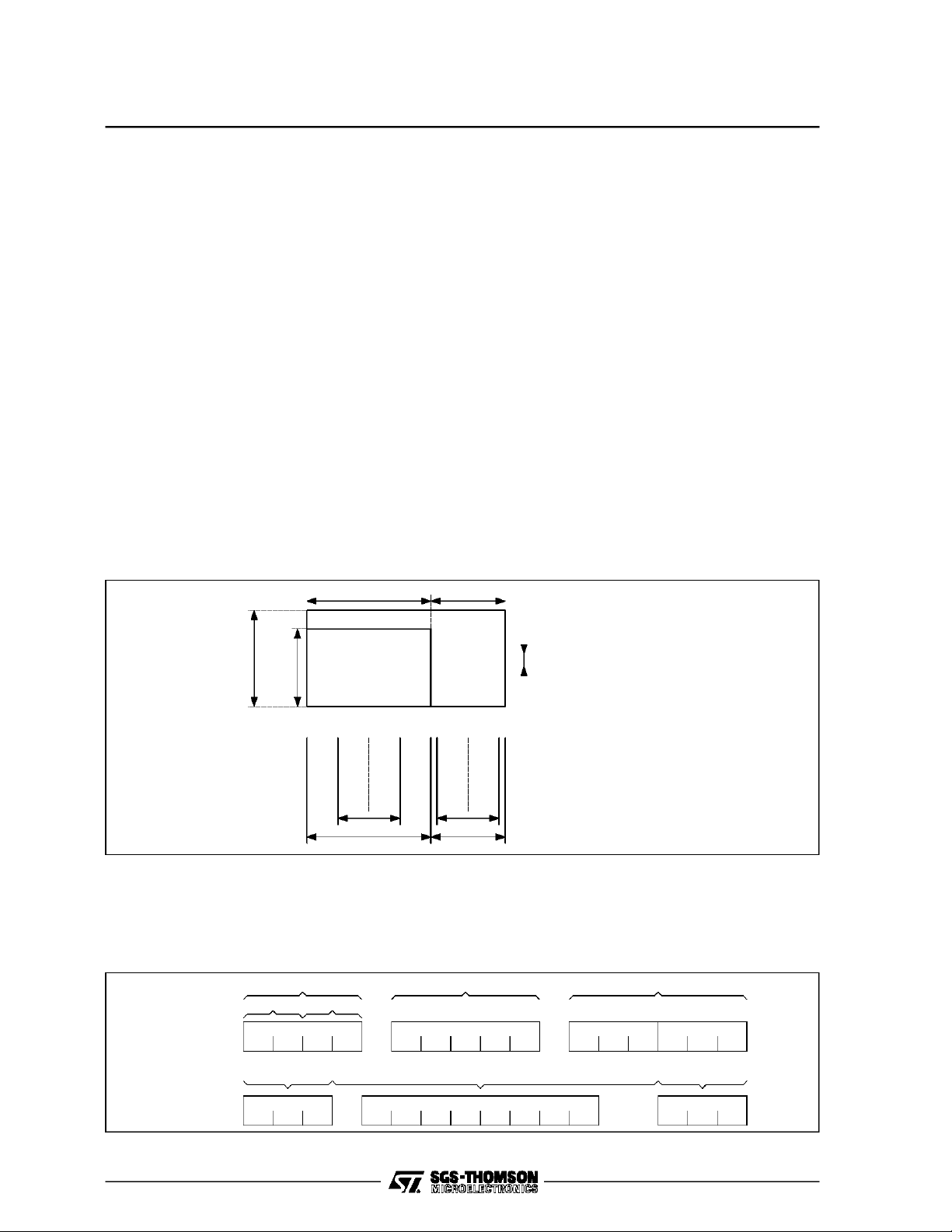
PACKAGE MECHANICAL DATA
40 PINS- PLASTICDIP
I
L
E
F
40
120
Dimensions
a1
b
b2
e3
D
e
21
Millimeters Inches
Min. Typ. Max. Min. Typ. Max.
a1 0.63 0.025
b 0.45 0.018
b1 0.23 0.31 0.009 0.012
b2 1.27 0.050
D 52.58 2.070
E 15.2 16.68 0.598 0.657
e 2.54 0.100
e3 48.26 1.900
F 14.1 0.555
i 4.445 0.175
L 3.3 0.130
b1
PM-DIP40.EPS
DIP40.TBL
Information furnished is believed to be accurate and reliable. However, SGS-THOMSON Microelectronics assumes no responsibility
for the consequences of use of such information nor for anyinfringement of patents or other rights of third parties which may result
from its use. Nolicence is granted by implication or otherwise under any patent or patent rights of SGS-THOMSON Microelectronics.
Specifications mentioned in this publication are subject to change without notice. This publication supersedes and replaces all
information previously supplied. SGS-THOMSON Microelectronics products are not authorized for use as critical components inlife
support devices or systems without express written approval of SGS-THOMSON Microelectronics.
1995 SGS-THOMSON Microelectronics - All RightsReserved
Purchase of I
2
I
C Patent. Rights to use these components in a I2C system, is granted provided that the system conforms to
Australia - Brazil - China - France - Germany - Hong Kong - Italy - Japan - Korea - Malaysia - Malta - Morocco
The Netherlands - Singapore - Spain - Sweden - Switzerland - Taiwan - Thailand - United Kingdom - U.S.A.
2
C Components of SGS-THOMSON Microelectronics, conveys alicense under the Philips
2
the I
C Standard Specifications as defined by Philips.
SGS-THOMSON Microelectronics GROUP OF COMPANIES
38/38
 Loading...