

Page 1
Ordering number : ENN6577
EC3H04B
NPN Epitaxial Planar Type Silicon Transistor
EC3H04B
High-Frequency Low-Noise Amplifier
and OSC Applications
Features
•
Low noise : NF=1.7dB typ (f=2GHz).
• High cut-off frequency : f
• Low operating voltage.
• Ultraminiature (1006 size) and thin (0.5mm)
leadless package.
=8GHz typ (VCE=1V).
T
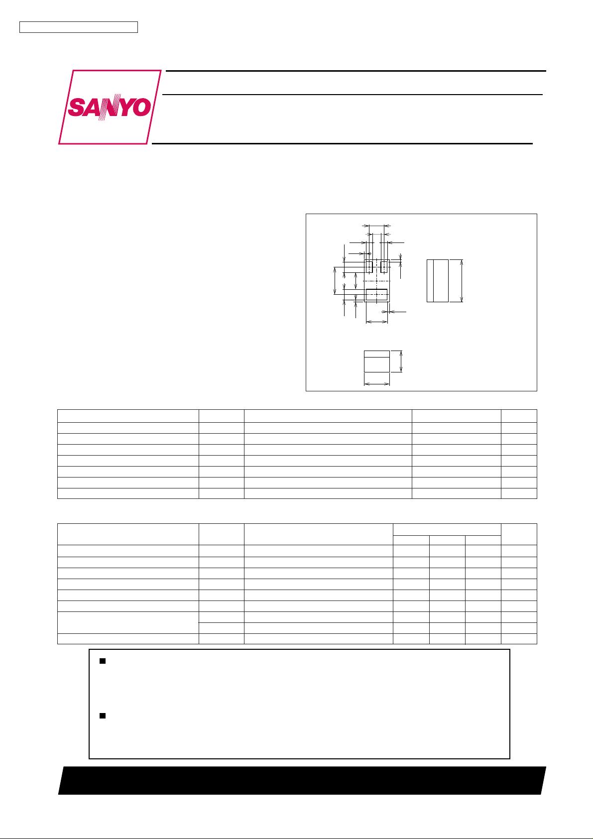
Package Dimensions
unit : mm
2183
0.25
0.65
0.25
0.35
0.15
0.05
1
0.4
0.05
(Bottom View)
0.2
3
0.5
[EC3H04B]
0.15
2
0.05
0.05
1.0
1 : Base
2 : Emitter
Specifications
0.5
0.6
3 : Collector
SANYO : E-CSP1006-3
Absolute Maximum Ratings at T a=25°C
Parameter Symbol Conditions Ratings Unit
Collector-to-Base Voltage V
Collector-to-Emitter Voltage V
Emitter-to-Base Voltage V
Collector Current I
Collector Dissipation P
Junction T emperature Tj 150 °C
Storage T emperature T stg --55 to +150 °C
CBO
CEO
EBO
C
C
9V
6V
2V
100 mA
100 mW
Electrical Characteristics at Ta=25°C
Parameter Symbol Conditions
Collector Cutoff Current I
Emitter Cutoff Current I
DC Current Gain h
Gain-Bandwidth Product f
Output Capacitance Cob VCB=1V, f=1MHz 1.1 1.5 pF
Reverse Transfer Capacitance Cre VCB=1V, f=1MHz 0.85 pF
Forward Transfer Gain
Noise Figure NF VCE=1V, IC=10mA, f=2GHz 1.7 2.5 dB
CBO
EBO
FE
S21e
S21e
VCB=5V, IE=0 1.0 µA
VEB=1V, IC=0 10 µA
VCE=1V, IC=10mA 100 180
VCE=1V, IC=10mA 6 8 GHz
T
2
1VCE=1V, IC=10mA, f=2GHz 4 5 dB
2
2VCE=3V, IC=20mA, f=1GHz 12 dB
Any and all SANYO products described or contained herein do not have specifications that can handle
applications that require extremely high levels of reliability, such as life-support systems, aircraft's
control systems, or other applications whose failure can be reasonably expected to result in serious
physical and/or material damage. Consult with your SANYO representative nearest you before using
any SANYO products described or contained herein in such applications.
SANYO assumes no responsibility for equipment failures that result from using products at values that
exceed, even momentarily, rated values (such as maximum ratings, operating condition ranges, or other
parameters) listed in products specifications of any and all SANYO products described or contained
herein.
Ratings
min typ max
SANYO Electric Co.,Ltd. Semiconductor Company
TOKYO OFFICE Tokyo Bldg., 1-10, 1 Chome, Ueno, Taito-ku, TOKYO, 110-8534 JAPAN
71400 TS IM TA-2478
No.6577-1/6
Unit
Page 2
EC3H04B
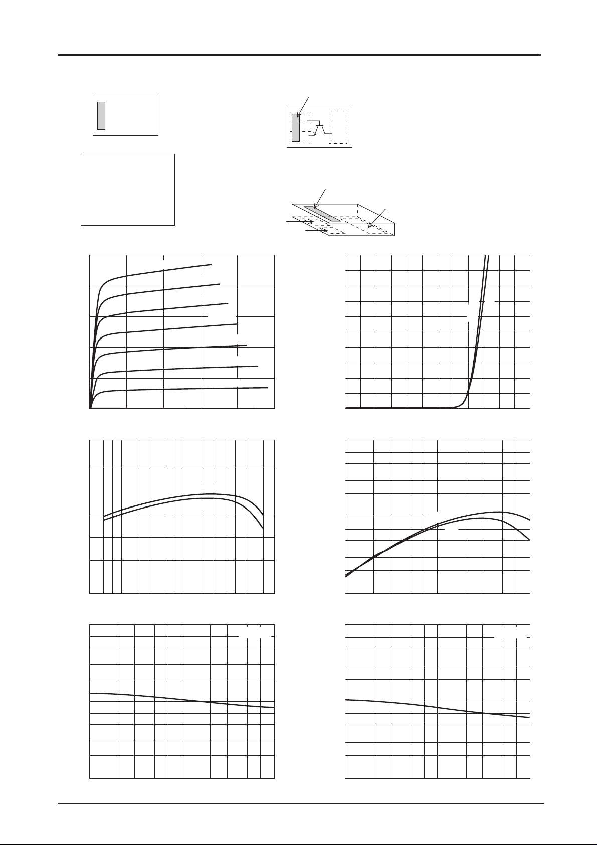
Type No. Indication (Top view) Electrical Connection (Top view)
Polarity nark (Top)
D
This product adopts a
high-frequency process.
Please be careful when
handling it beause it is
susceptible to static
electricity.
50
40
-- mA
C
30
20
Collector Current, I
10
0
0
3
2
FE
100
7
DC Current Gain, h
5
3
3
10
7
5
3
2
1
Collector-to-Emitter Voltage, VCE -- V
7
5
1.0
I
C -- VCE
0.35mA
0.30mA
0.25mA
0.20mA
0.15mA
32
h
FE -- IC
VCE=3V
1V
3
2
7
5
3
2
Collector Current, IC -- mA
Cob -- V
CB
0.10mA
0.05mA
4
7
5
IB=0
IT02220
100
IT02222
f=1MHz
Base
Emitter
Base
5
2103
Polarity mark (Top)
Emitter
Collector
*Electrodes : on the bottom
Collector
100
90
80
70
-- mA
C
60
50
40
30
Collector Current, I
20
10
0
0
0.2 0.4 0.6 0.8 1.0 1.20.1 0.3 0.5 0.7 0.9 1.1
Base-to-Emitter V oltage, VBE -- V
100
7
5
3
-- GHz
T
2
10
7
5
3
2
Gain-Bandwidth Product, f
1.0
1.0
2
3
Collector Current, IC -- mA
10
7
5
3
2
I
C -- VBE
fT -- I
V
CE
57
10
Cre -- V
=3V
CE
V
C
=3V
1V
2357
CB
1V
IT02221
100
IT02223
f=1MHz
Output Capacitance, Cob -- pF
1.0
0.1
1.0
7
5
3
2
7
5
3
2
Reverse Transfer Capacitance, Cre -- pF
0.1
2
5
3
7
1.0
Collector-to-Base Voltage, V
2
CB --
5
3
7
10
IT02224
V
0.1
0.1
23 57 23 57
Collector-to-Base Voltage, V
1.0
CB --
IT02225
V
10
No.6577-2/6
Page 3

EC3H04B
16
14
-- dB
2
12
10
8
6
4
2
Forward Transfer Gain, S21e
0
1.0
5.0
4.5
4.0
dB
3.5
--
3.0
2.5
2.0
1.5
Noise Figure, NF
1.0
0.5
0
1.0
S21e2 -- I
V
CE
3
2
7
5
10
Collector Current, IC -- mA
NF -- I
532
7
Collector Current, IC -- mA
10
1V
=3V
C
C
16
f=1GHz
14
-- dB
2
12
10
8
6
S21e2 -- I
=3V
V
CE
C
f=2GHz
1V
4
2
Forward Transfer Gain, S21e
3
2
7
5
100
IT02226 IT02227
VCE=1V
f=2GHz
532
7
100
IT02228
0
120
100
-- mW
80
C
60
40
20
Collector Dissipation, P
0
1.0
0
23 5
Collector Current, IC -- mA
4020
Ambient Temperature, Ta -- °C
P
7
C
10
-- Ta
23 5
100 12060 80
140
7
IT02229
100
160
S Parameters (Common emitter)
VCE=1V, IC=1mA, ZO=50Ω
Freq(MHz)
200 0.925 --41.9 2.875 149.0 0.113 63.2 0.913 --21.9
400 0.835 --78.1 2.702 124.4 0.180 43.8 0.780 --36.1
600 0.758 --101.3 2.125 106.7 0.201 31.3 0.660 --44.2
800 0.716 --115.7 1.584 97.7 0.218 21.4 0.613 --50.5
1000 0.729 --129.3 1.443 83.8 0.224 16.9 0.560 --58.6
1200 0.706 --140.2 1.328 74.8 0.217 13.4 0.550 --62.4
1400 0.707 --146.9 1.142 67.8 0.209 9.9 0.569 --66.0
1600 0.716 --151.9 0.980 61.1 0.203 7.2 0.548 --72.5
1800 0.698 --157.2 0.871 53.1 0.196 4.9 0.529 --77.0
2000 0.702 --164.2 0.877 52.1 0.177 9.6 0.560 --84.6
2200 0.700 --167.0 0.759 42.9 0.173 5.7 0.536 --87.6
2400 0.704 --172.3 0.744 43.0 0.156 13.7 0.588 --94.5
2600 0.704 --175.5 0.673 35.5 0.150 12.7 0.553 --98.5
2800 0.708 --179.8 0.652 35.8 0.143 23.7 0.615 --104.0
3000 0.709 177.0 0.604 30.5 0.142 25.3 0.575 --109.0
S
11
∠S
S
11
21
∠S
S
21
12
∠S
S
12
22
∠S
22
No.6577-3/6
Page 4

EC3H04B
VCE=1V, IC=5mA, ZO=50Ω
Freq(MHz)
200 0.744 --82.8 10.317 130.5 0.083 49.0 0.696 --53.9
400 0.670 --122.0 6.592 108.4 0.105 36.0 0.462 --79.7
600 0.618 --141.5 4.594 98.8 0.112 32.7 0.344 --93.5
800 0.624 --152.3 3.565 90.3 0.122 32.6 0.297 --104.0
1000 0.627 --160.5 2.967 82.3 0.126 34.6 0.278 --111.7
1200 0.623 --165.9 2.504 76.9 0.132 37.0 0.265 --118.5
1400 0.621 --170.1 2.167 72.1 0.140 39.1 0.258 --124.4
1600 0.621 --174.2 1.932 67.6 0.148 40.3 0.261 --127.6
1800 0.614 --177.8 1.731 64.0 0.158 42.3 0.263 --131.6
2000 0.619 179.2 1.590 60.1 0.165 44.1 0.269 --133.5
2200 0.615 176.1 1.464 56.3 0.175 45.6 0.278 --137.0
2400 0.618 173.8 1.367 52.9 0.186 47.0 0.284 --138.7
2600 0.616 170.6 1.283 49.4 0.197 48.1 0.300 --141.1
2800 0.619 168.7 1.209 46.5 0.209 48.6 0.302 --143.1
3000 0.619 165.8 1.150 43.2 0.221 49.2 0.319 --144.9
VCE=1V, IC=10mA, ZO=50Ω
Freq(MHz)
200 0.661 --108.8 13.770 119.9 0.064 44.3 0.568 --77.3
400 0.631 --141.8 7.901 101.6 0.078 39.0 0.383 --108.6
600 0.610 --156.0 5.378 94.8 0.088 40.0 0.311 --125.2
800 0.610 --164.7 4.111 87.7 0.099 44.1 0.288 --136.7
1000 0.616 --170.2 3.376 81.1 0.109 47.8 0.283 --144.2
1200 0.615 --174.4 2.848 76.4 0.122 50.3 0.280 --149.7
1400 0.613 --177.9 2.468 72.3 0.134 52.1 0.280 --154.3
1600 0.613 179.0 2.191 68.5 0.148 53.1 0.281 --156.9
1800 0.608 176.0 1.967 65.4 0.162 53.6 0.284 --159.6
2000 0.608 173.6 1.791 61.9 0.175 54.2 0.286 --161.4
2200 0.607 170.9 1.659 58.6 0.188 54.7 0.294 --163.0
2400 0.606 168.8 1.540 55.3 0.202 54.4 0.296 --164.8
2600 0.606 166.2 1.450 52.4 0.217 54.1 0.303 --165.3
2800 0.605 164.3 1.365 49.2 0.231 53.9 0.306 --167.0
3000 0.607 162.0 1.297 46.5 0.245 53.2 0.313 --167.6
S
11
S
11
∠S
∠S
S
11
11
21
S
21
∠S
∠S
S
21
21
12
S
12
∠S
∠S
S
12
12
22
S
22
∠S
∠S
22
22
VCE=1V, IC=20mA, ZO=50Ω
Freq(MHz)
S
11
∠S
S
11
21
∠S
S
21
12
∠S
S
12
22
200 0.623 --131.3 15.796 111.7 0.048 43.6 0.484 --100.8
400 0.623 --156.5 8.545 96.9 0.061 45.9 0.370 --132.7
600 0.613 --166.4 5.750 91.9 0.074 50.6 0.333 --147.4
800 0.615 --172.4 4.375 86.0 0.089 54.4 0.326 --156.2
1000 0.620 --176.6 3.571 80.0 0.103 58.0 0.328 --162.1
1200 0.619 --180.0 3.011 75.9 0.120 59.8 0.328 --166.1
1400 0.617 177.0 2.609 72.2 0.136 60.8 0.329 --169.3
1600 0.616 174.5 2.311 68.8 0.152 60.9 0.330 --171.7
1800 0.613 171.9 2.072 66.0 0.168 60.3 0.332 --174.0
2000 0.611 169.7 1.889 62.8 0.183 60.0 0.334 --175.5
2200 0.609 167.4 1.745 59.6 0.199 59.5 0.335 --176.8
2400 0.608 165.3 1.624 56.6 0.215 58.6 0.337 --178.2
2600 0.608 163.0 1.524 53.8 0.230 57.8 0.341 --179.0
2800 0.605 161.2 1.439 50.9 0.246 56.7 0.342 179.8
3000 0.606 159.3 1.365 48.2 0.261 55.6 0.344 179.1
∠S
22
No.6577-4/6
Page 5

EC3H04B
VCE=3V, IC=1mA, ZO=50Ω
Freq(MHz)
200 0.932 --38.6 3.040 152.2 0.088 65.7 0.943 --16.1
400 0.868 --69.7 2.804 129.9 0.143 47.6 0.845 --27.4
600 0.767 --92.6 2.258 113.8 0.166 33.5 0.733 --33.9
800 0.750 --111.5 1.795 101.5 0.187 27.4 0.671 --43.1
1000 0.736 --125.2 1.690 89.7 0.189 21.1 0.649 --47.0
1200 0.731 --134.4 1.409 80.9 0.182 17.0 0.631 --50.2
1400 0.734 --141.5 1.161 73.6 0.181 14.2 0.605 --55.7
1600 0.720 --148.8 1.098 66.8 0.179 10.9 0.587 --61.7
1800 0.708 --154.8 1.000 60.3 0.166 11.7 0.590 --65.4
2000 0.707 --160.8 0.926 57.7 0.154 12.4 0.598 --70.5
2200 0.704 --164.9 0.868 49.7 0.146 14.0 0.594 --75.1
2400 0.711 --170.0 0.784 49.1 0.137 18.1 0.612 --80.3
2600 0.703 --173.6 0.775 41.7 0.129 22.6 0.607 --85.1
2800 0.715 --177.9 0.677 41.8 0.127 29.7 0.629 --89.8
3000 0.702 178.8 0.703 36.0 0.126 36.4 0.627 --95.1
VCE=3V, IC=5mA, ZO=50Ω
Freq(MHz)
200 0.762 --71.5 11.124 135.7 0.068 53.9 0.752 --41.9
400 0.670 --111.1 7.524 113.1 0.090 40.4 0.516 --61.8
600 0.604 --132.1 5.338 102.6 0.100 35.6 0.379 --70.5
800 0.605 --145.2 4.172 93.9 0.108 36.0 0.320 --78.9
1000 0.604 --154.3 3.488 85.6 0.113 37.6 0.286 --84.5
1200 0.601 --160.4 2.943 80.0 0.118 39.7 0.264 --88.7
1400 0.599 --165.3 2.535 75.2 0.125 41.7 0.251 --93.6
1600 0.597 --169.8 2.265 70.8 0.133 43.7 0.247 --98.3
1800 0.590 --173.6 2.027 67.0 0.140 45.8 0.244 --101.4
2000 0.594 --177.1 1.853 63.4 0.150 47.8 0.250 --105.1
2200 0.590 179.9 1.711 59.2 0.158 49.5 0.253 --108.4
2400 0.594 177.0 1.584 56.1 0.168 50.8 0.264 --111.4
2600 0.593 174.1 1.493 52.3 0.179 51.9 0.270 --114.9
2800 0.597 171.7 1.393 49.5 0.191 53.0 0.281 --117.2
3000 0.594 169.0 1.333 46.1 0.203 53.6 0.290 --120.8
S
11
S
11
∠S
∠S
S
11
11
21
S
21
∠S
∠S
S
21
21
12
S
12
∠S
∠S
S
12
12
22
S
22
∠S
∠S
22
22
VCE=3V, IC=10mA, ZO=50Ω
Freq(MHz)
S
11
∠S
S
11
21
∠S
S
21
12
∠S
S
12
22
200 0.660 --94.3 15.608 125.5 0.054 49.6 0.618 --60.0
400 0.603 --131.8 9.377 105.6 0.069 42.5 0.389 --84.8
600 0.572 --148.7 6.448 97.9 0.079 43.2 0.284 --97.7
800 0.570 --158.0 4.947 90.6 0.089 46.3 0.242 --108.4
1000 0.576 --164.8 4.073 83.7 0.099 49.9 0.223 --116.7
1200 0.575 --169.6 3.433 78.9 0.110 52.4 0.211 --122.8
1400 0.572 --173.7 2.965 74.9 0.121 54.5 0.205 --128.1
1600 0.571 --177.1 2.628 71.0 0.134 55.7 0.205 --131.6
1800 0.568 179.7 2.353 67.9 0.146 56.4 0.205 --135.1
2000 0.569 177.2 2.141 64.5 0.158 56.9 0.208 --137.3
2200 0.568 174.4 1.977 61.1 0.172 57.3 0.214 --139.7
2400 0.568 172.2 1.828 57.9 0.185 57.6 0.219 --141.3
2600 0.569 169.5 1.718 54.8 0.198 57.4 0.228 --143.1
2800 0.569 167.6 1.611 51.8 0.212 57.4 0.233 --144.4
3000 0.572 165.4 1.530 49.0 0.226 56.9 0.242 --145.8
∠S
22
No.6577-5/6
Page 6

EC3H04B
VCE=3V, IC=20mA, ZO=50Ω
Freq(MHz)
200 0.587 --116.9 18.878 117.0 0.042 48.5 0.505 --78.6
400 0.571 --147.6 10.531 100.4 0.055 48.9 0.325 --107.8
600 0.556 --160.0 7.129 94.6 0.068 52.3 0.256 --123.6
800 0.558 --167.1 5.430 88.4 0.081 55.9 0.234 --135.0
1000 0.564 --172.2 4.435 82.3 0.094 60.1 0.227 --143.1
1200 0.563 --175.9 3.735 78.1 0.108 61.6 0.224 --148.6
1400 0.561 --179.2 3.225 74.5 0.123 62.8 0.222 --152.9
1600 0.561 178.1 2.853 71.1 0.138 62.9 0.223 --155.7
1800 0.558 175.3 2.549 68.3 0.153 62.6 0.224 --158.4
2000 0.558 173.1 2.320 65.2 0.167 62.3 0.227 --160.2
2200 0.558 170.8 2.136 62.1 0.183 62.0 0.230 --161.5
2400 0.556 168.7 1.981 59.0 0.197 61.3 0.234 --163.0
2600 0.558 166.4 1.854 56.2 0.212 60.6 0.241 --163.6
2800 0.557 164.7 1.743 53.3 0.226 59.7 0.243 --164.5
3000 0.559 162.6 1.648 50.7 0.240 58.6 0.249 --165.2
S
11
∠S
S
11
21
∠S
S
21
12
∠S
S
12
22
∠S
22
Specifications of any and all SANYO products described or contained herein stipulate the performance,
characteristics, and functions of the described products in the independent state, and are not guarantees
of the performance, characteristics, and functions of the described products as mounted in the customer's
products or equipment. To verify symptoms and states that cannot be evaluated in an independent device,
the customer should always evaluate and test devices mounted in the customer's products or equipment.
SANYO Electric Co., Ltd. strives to supply high-quality high-reliability products. However, any and all
semiconductor products fail with some probability. It is possible that these probabilistic failures could
give rise to accidents or events that could endanger human lives, that could give rise to smoke or fire,
or that could cause damage to other property. When designing equipment, adopt safety measures so
that these kinds of accidents or events cannot occur. Such measures include but are not limited to protective
circuits and error prevention circuits for safe design, redundant design, and structural design.
In the event that any or all SANYO products(including technical data,services) described or
contained herein are controlled under any of applicable local export control laws and regulations,
such products must not be exported without obtaining the export license from the authorities
concerned in accordance with the above law.
No part of this publication may be reproduced or transmitted in any form or by any means, electronic or
mechanical, including photocopying and recording, or any information storage or retrieval system,
or otherwise, without the prior written permission of SANYO Electric Co. , Ltd.
Any and all information described or contained herein are subject to change without notice due to
product/technology improvement, etc. When designing equipment, refer to the "Delivery Specification"
for the SANYO product that you intend to use.
Information (including circuit diagrams and circuit parameters) herein is for example only ; it is not
guaranteed for volume production. SANYO believes information herein is accurate and reliable, but
no guarantees are made or implied regarding its use or any infringements of intellectual property rights
or other rights of third parties.
This catalog provides information as of July, 2000. Specifications and information herein are subject
to change without notice.
PS
No.6577-6/6
 Loading...