

Page 1
Ordering number : ENN6579
EC3H02C
NPN Epitaxial Planar Silicon Transistor
EC3H02C
VHF to UHF Wide-Band Low-Noise
Amplifier Applications
Features
•
Low noise : NF=1.0dB typ (f=1GHz).
• High gain :S21e
• High cutoff frequency : f
• Ultraminiature (1008 size) and thin (0.6mm)
leadless package .
2
=12dB typ (f=1GHz).
=7GHz typ.
T
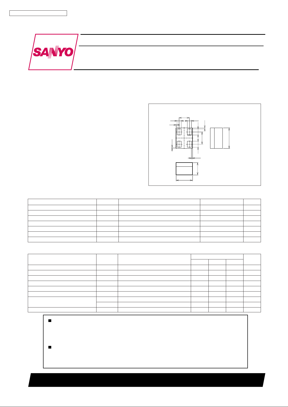
Package Dimensions
unit : mm
2184
[EC3H02C]
0.5
0.2 0.2
0.05
3
2
0.05
(Bottom View)
0.3
4
0.6
1
0.3
0.05
0.05
1.0
1 : Base
2 : Emitter
0.6
0.8
3 : Collector
4 : Collector
SANYO : E-CSP1008-4
Specifications
Absolute Maximum Ratings at T a=25°C
Parameter Symbol Conditions Ratings Unit
Collector-to-Base Voltage V
Collector-to-Emitter Voltage V
Emitter-to-Base Voltage V
Collector Current I
Collector Dissipation P
Junction T emperature Tj 150 °C
Storage T emperature T stg --55 to +150 °C
CBO
CEO
EBO
C
C
20 V
10 V
2V
70 mA
100 mW
Electrical Characteristics at Ta=25°C
Parameter Symbol Conditions
Collector Cutoff Current I
Emitter Cutoff Current I
DC Current Gain h
Gain-Bandwitch Product f
Output Capacitance Cob VCB=10V , f=1MHz 0.7 1.2 pF
Reverse Transfer Capacitance Cre VCB=10V , f=1MHz 0.45 pF
Forward Transfer Gain
Noise Figure NF VCE=5V, IC=7mA, f=1GHz 1.0 1.8 dB
CBO
EBO
FE
S21e
S21e
VCB=10V, IE=0 1.0 µA
VEB=1V, IC=0 10 µA
VCE=5V, IC=20mA 100 180
VCE=5V, IC=20mA 5 7 GHz
T
2
1VCE=5V, IC=20mA, f=1GHz 9 12 dB
2
2VCE=2V, IC=3mA, f=1GHz 8.5 dB
Any and all SANYO products described or contained herein do not have specifications that can handle
applications that require extremely high levels of reliability, such as life-support systems, aircraft's
control systems, or other applications whose failure can be reasonably expected to result in serious
physical and/or material damage. Consult with your SANYO representative nearest you before using
any SANYO products described or contained herein in such applications.
SANYO assumes no responsibility for equipment failures that result from using products at values that
exceed, even momentarily, rated values (such as maximum ratings, operating condition ranges, or other
parameters) listed in products specifications of any and all SANYO products described or contained
herein.
Ratings
min typ max
SANYO Electric Co.,Ltd. Semiconductor Company
TOKYO OFFICE Tokyo Bldg., 1-10, 1 Chome, Ueno, Taito-ku, TOKYO, 110-8534 JAPAN
71400 TS IM TA-2739
No.6579-1/5
Unit
Page 2
EC3H02C
Type No. Indication (Top view) Electrical Connection (Top view)
Polarity mark (Top)
B
This product adopts a
high-frequency process.
Please be careful when
handling it beause it is
susceptible to static
electricity.
3
2
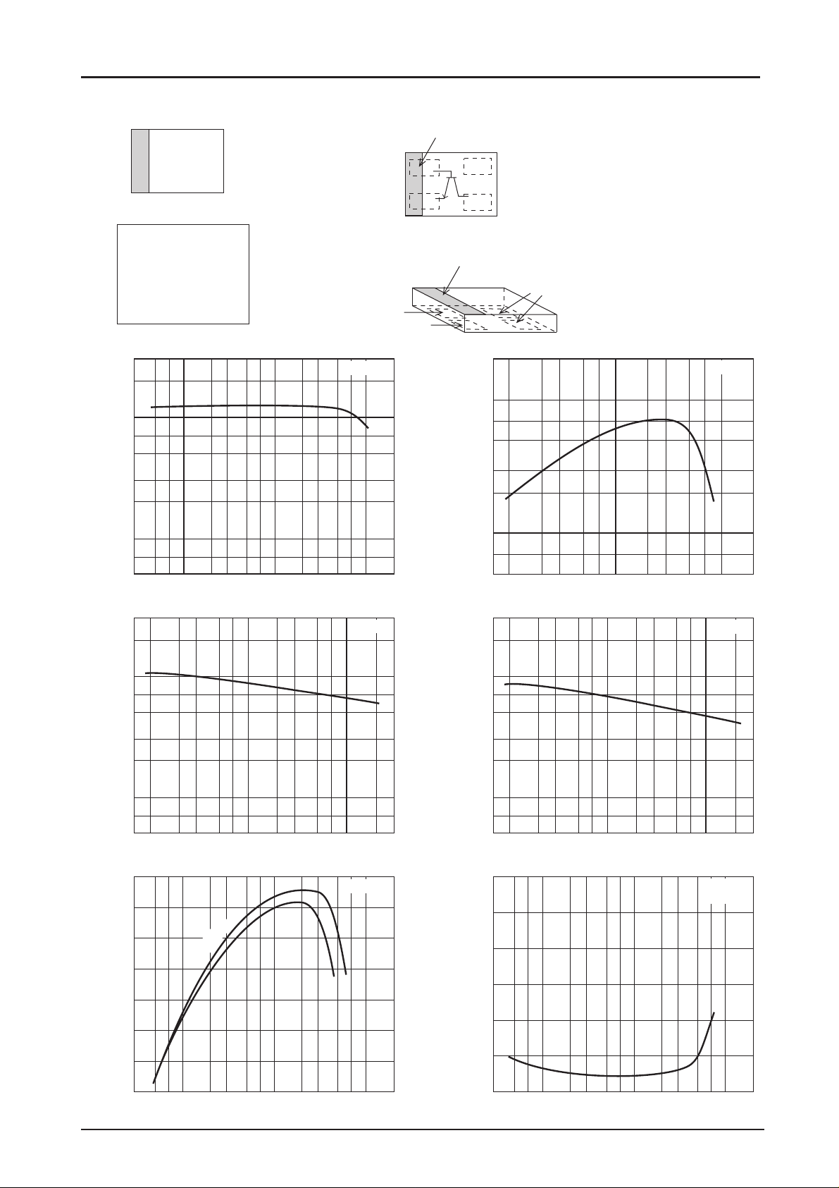
100
FE
7
5
3
2
DC Current Gain, h
10
7
5
3
2
1.0
hFE -- I
32
C
57 32257357
10 100
Collector Current, IC -- mA
Cob -- V
CB
Base
Emitter
Base
VCE=5V
IT01363
f=1MHz
Polarity mark (Top)
Emitter
Collector
*Electrodes : on the bottom
Collector
2
10
-- GHz
7
T
5
3
2
1.0
Gain-Bandwidth Product, f
7
5
7223 5723 57
1.0
Collector Current, IC -- mA
3
2
f
-- I
T
C
10 100
Cre -- V
CB
VCE=5V
IT01364
f=1MHz
1.0
7
5
3
2
Output Capacitance, Cob -- pF
0.1
7
5
325
Collector-to-Base Voltage, V
14
12
-- dB
2
10
8
6
4
2
Forward Transfer Gain, S21e
0
33257
CE
V
1.0
Collector Current, IC -- mA
73257 327
1.0
S21e2 -- I
=5V
2V
10
100.1
V
CB --
IT01365
C
f=1GHz
325757 2
100
IT01367
1.0
7
5
3
2
0.1
7
Reverse Transfer Capacitance, Cre -- pF
5
12
10
dB
8
--
6
4
Noise Figure, NF
2
0
325
73257 327
Collector-to-Base Voltage, V
1.0
1.0
NF -- I
32
57 32257357
C
10 100
Collector Current, IC -- mA
CB --
100.1
V
IT01366
VCE=5V
f=1GHz
IT01368
No.6579-2/5
Page 3

EC3H02C
P
-- Ta
120
100
-- mW
80
C
60
40
20
Collector Dissipation, P
0
2006040 80 100 140120 160
Ambient Temperature, Ta -- °C
S Parameters (Common emitter)
VCE=1V, IC=1mA, ZO=50Ω
Freq(MHz)
100 0.955 --22.6 3.418 163.3 0.056 76.0 0.975 --10.5
200 0.922 --43.0 3.109 148.7 0.104 63.2 0.921 --19.6
400 0.845 --77.2 2.617 124.8 0.165 44.2 0.794 --32.9
600 0.782 --101.8 2.156 107.7 0.189 31.3 0.694 --41.5
800 0.746 --119.1 1.788 94.2 0.200 23.5 0.630 --47.7
1000 0.734 --131.1 1.498 83.7 0.201 17.7 0.596 --52.2
1200 0.717 --141.2 1.326 74.6 0.198 14.7 0.573 --57.6
1400 0.707 --148.9 1.154 66.6 0.193 12.0 0.559 --61.9
1600 0.708 --155.5 1.029 60.2 0.182 10.7 0.561 --66.1
1800 0.711 --161.6 0.953 54.6 0.171 10.8 0.561 --71.6
2000 0.712 --166.5 0.880 49.3 0.160 13.0 0.569 --76.5
C
IT01369
S
11
∠S
S
11
21
∠S
S
21
12
∠S
S
12
22
∠S
22
VCE=1V, IC=5mA, ZO=50Ω
Freq(MHz)
S
11
∠S
S
11
21
∠S
S
21
12
∠S
S
12
22
100 0.818 --47.9 13.330 150.0 0.049 64.3 0.869 --29.8
200 0.739 --83.2 10.545 129.6 0.076 49.6 0.681 --50.0
400 0.661 --122.9 6.688 107.4 0.098 37.8 0.445 --71.3
600 0.627 --142.2 4.726 95.9 0.106 35.4 0.334 --81.7
800 0.616 --153.8 3.653 87.5 0.114 36.3 0.279 --89.2
1000 0.614 --161.8 2.989 80.7 0.122 38.4 0.252 --94.7
1200 0.611 --167.3 2.534 75.1 0.130 40.8 0.238 --99.0
1400 0.607 --172.2 2.207 70.1 0.139 43.1 0.231 --102.8
1600 0.607 --176.6 1.965 65.5 0.149 45.1 0.227 --106.4
1800 0.610 179.8 1.776 61.1 0.159 47.1 0.230 --109.8
2000 0.609 176.9 1.627 57.0 0.171 48.6 0.237 --112.1
VCE=2V, IC=3mA, ZO=50Ω
Freq(MHz)
S
11
∠S
S
11
21
∠S
S
21
12
∠S
S
12
22
100 0.890 --32.1 9.129 158.3 0.042 72.1 0.938 --17.1
200 0.827 --59.6 7.989 141.0 0.073 57.6 0.824 --30.2
400 0.725 --98.7 5.823 117.5 0.104 41.8 0.618 --45.5
600 0.666 --121.9 4.355 103.4 0.115 34.5 0.496 --52.3
800 0.641 --136.9 3.448 93.1 0.121 32.2 0.429 --56.5
1000 0.631 --147.3 2.854 85.1 0.125 32.0 0.392 --59.9
1200 0.624 --154.9 2.436 78.5 0.128 33.1 0.372 --62.9
1400 0.618 --161.3 2.124 72.8 0.131 35.2 0.360 --66.0
1600 0.616 --166.7 1.894 67.5 0.134 37.6 0.352 --69.1
1800 0.618 --171.4 1.715 62.7 0.139 40.3 0.351 --72.9
2000 0.618 --175.1 1.571 58.1 0.144 43.2 0.357 --76.4
∠S
∠S
22
22
No.6579-3/5
Page 4

EC3H02C
VCE=2V, IC=10mA, ZO=50Ω
Freq(MHz)
100 0.715 --60.8 21.486 143.7 0.035 62.1 0.806 --36.1
200 0.643 --98.6 15.499 122.8 0.051 49.2 0.580 --56.8
400 0.589 --135.1 9.112 103.3 0.065 44.8 0.355 --75.8
600 0.570 --151.5 6.296 93.9 0.075 47.3 0.261 --84.5
800 0.564 --161.1 4.816 86.9 0.087 50.9 0.215 --90.9
1000 0.563 --167.7 3.921 81.1 0.098 53.6 0.192 --95.4
1200 0.560 --172.3 3.308 76.3 0.112 56.0 0.181 --99.0
1400 0.558 --176.2 2.867 72.1 0.125 57.7 0.172 --102.6
1600 0.558 180.0 2.550 68.1 0.139 58.8 0.169 --105.3
1800 0.562 176.8 2.293 64.2 0.155 59.5 0.170 --107.8
2000 0.561 174.4 2.092 60.5 0.169 59.8 0.176 --109.2
VCE=5V, IC=7mA, ZO=50Ω
Freq(MHz)
100 0.797 --42.9 17.630 152.0 0.030 68.4 0.892 --22.3
200 0.708 --76.1 14.170 132.4 0.048 55.1 0.723 --36.7
400 0.608 --116.0 9.186 110.4 0.064 45.4 0.494 --48.9
600 0.565 --136.4 6.534 98.9 0.073 44.6 0.385 --52.5
800 0.550 --148.8 5.055 90.8 0.081 46.8 0.329 --54.0
1000 0.547 --157.0 4.134 84.3 0.089 49.9 0.299 --55.4
1200 0.541 --163.2 3.497 79.0 0.098 52.4 0.285 --56.7
1400 0.537 --168.1 3.025 74.4 0.109 55.0 0.277 --57.9
1600 0.539 --172.5 2.687 70.0 0.119 57.0 0.270 --60.1
1800 0.540 --176.5 2.425 65.8 0.130 58.6 0.271 --63.0
2000 0.540 --179.4 2.212 61.9 0.142 59.9 0.277 --65.8
S
11
S
11
∠S
∠S
S
11
11
21
S
21
∠S
∠S
S
21
21
12
S
12
∠S
∠S
S
12
12
22
S
22
∠S
∠S
22
22
VCE=5V, IC=20mA, ZO=50Ω
Freq(MHz)
S
11
∠S
S
11
21
∠S
S
21
12
∠S
S
12
22
100 0.618 --71.5 30.252 138.1 0.023 60.6 0.748 --37.0
200 0.554 --110.5 20.311 117.7 0.034 52.7 0.511 --52.9
400 0.519 --143.1 11.419 100.5 0.046 54.5 0.306 --62.6
600 0.507 --156.8 7.810 92.4 0.058 58.7 0.230 --64.0
800 0.504 --165.0 5.941 86.2 0.071 62.2 0.193 --64.9
1000 0.505 --170.5 4.816 81.1 0.084 64.7 0.175 --66.0
1200 0.504 --174.3 4.051 76.8 0.098 66.2 0.167 --67.0
1400 0.502 --177.8 3.502 73.0 0.112 67.2 0.162 --68.2
1600 0.504 178.9 3.107 69.3 0.127 67.4 0.159 --70.1
1800 0.508 176.0 2.788 65.7 0.142 67.4 0.161 --72.4
2000 0.507 173.9 2.539 62.3 0.155 67.1 0.169 --74.8
∠S
22
No.6579-4/5
Page 5

EC3H02C
Specifications of any and all SANYO products described or contained herein stipulate the performance,
characteristics, and functions of the described products in the independent state, and are not guarantees
of the performance, characteristics, and functions of the described products as mounted in the customer's
products or equipment. To verify symptoms and states that cannot be evaluated in an independent device,
the customer should always evaluate and test devices mounted in the customer's products or equipment.
SANYO Electric Co., Ltd. strives to supply high-quality high-reliability products. However, any and all
semiconductor products fail with some probability. It is possible that these probabilistic failures could
give rise to accidents or events that could endanger human lives, that could give rise to smoke or fire,
or that could cause damage to other property. When designing equipment, adopt safety measures so
that these kinds of accidents or events cannot occur. Such measures include but are not limited to protective
circuits and error prevention circuits for safe design, redundant design, and structural design.
In the event that any or all SANYO products(including technical data,services) described or
contained herein are controlled under any of applicable local export control laws and regulations,
such products must not be exported without obtaining the export license from the authorities
concerned in accordance with the above law.
No part of this publication may be reproduced or transmitted in any form or by any means, electronic or
mechanical, including photocopying and recording, or any information storage or retrieval system,
or otherwise, without the prior written permission of SANYO Electric Co. , Ltd.
Any and all information described or contained herein are subject to change without notice due to
product/technology improvement, etc. When designing equipment, refer to the "Delivery Specification"
for the SANYO product that you intend to use.
Information (including circuit diagrams and circuit parameters) herein is for example only ; it is not
guaranteed for volume production. SANYO believes information herein is accurate and reliable, but
no guarantees are made or implied regarding its use or any infringements of intellectual property rights
or other rights of third parties.
This catalog provides information as of July, 2000. Specifications and information herein are subject
to change without notice.
No.6579-5/5
PS
 Loading...