

Page 1
Any and all SANYO products described or contained herein do not have specifications that can handle
applications that require extremely high levels of reliability, such as life-support systems, aircraft’s
control systems, or other applications whose failure can be reasonably expected to result in serious
physical and/or material damage. Consult with your SANYO representative nearest you before using
any SANYO products described or contained herein in such applications.
SANYO assumes no responsibility for equipment failures that result from using products at values that
exceed, even momentarily, rated values (such as maximum ratings, operating condition ranges,or other
parameters) listed in products specifications of any and all SANYO products described or contained
herein.
NPN Epitaxial Planar Silicon Transistor
VHF to UHF Low-Noise Wide-Band
Amplifier Applications
Ordering number:ENN6523
EC3H02B
SANYO Electric Co.,Ltd. Semiconductor Company
TOKYO OFFICE Tokyo Bldg., 1-10, 1 Chome, Ueno, Taito-ku, TOKYO, 110-8534 JAPAN
Features
· Low noise : NF=1.0dB typ (f=1GHz).
· High gain : S21e2=12dB typ (f=1GHz).
· High cutoff frequency : fT=7GHz typ.
· Ultrasmall (1006size), slim (0.5mm) leadless package.
Specifications
Absolute Maximum Ratings at Ta = 25˚C
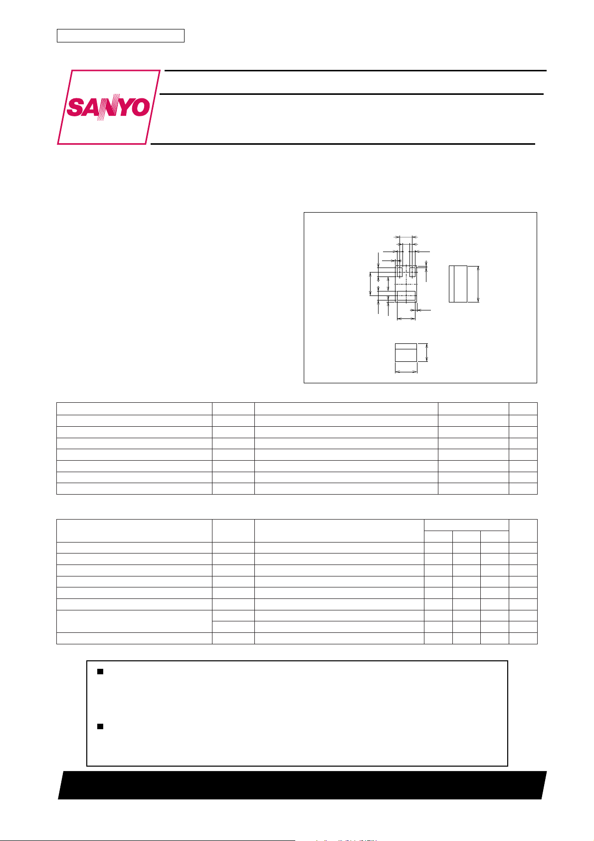
Package Dimensions
unit:mm
2183
[EC3H02B]
0.35
0.2
1
3
0.5
(Bottom view)
0.6
0.15
2
0.05
0.05
1 : Base
0.5
2 : Emitter
3 : Collector
SANYO : E-CSP1006-3
0.15
0.05
0.25
0.4
0.65
0.25
0.05
retemaraPlobmySsnoitidnoCsgnitaRtinU
egatloVesaB-ot-rotcelloCV
egatloVrettimE-ot-rotcelloCV
egatloVesaB-ot-rettimEV
tnerruCrotcelloCI
noitapissiDrotcelloCP
erutarepmeTnoitcnuJjT 051
erutarepmeTegarotSgtsT 051+ot55–
OBC
OEC
OBE
C
C
1.0
02V
01V
2V
07Am
001Wm
˚C
˚C
Electrical Characteristics at Ta = 25˚C
retemaraPlobmySsnoitidnoC
tnerruCffotuCrotcelloCI
tnerruCffotuCrettimEI
niaGtnerruCCD
tcudorPhtdiwdnaB-niaG
ecnaticapaCtuptuOboCV
ecnaticapaCrefsnarTesreveRerCV
niaGrefsnarTdrawroF
erugiFesioN
h
V
OBC
V
OBE
V
EF
f
V
T
2
V
|e12S|
1
2
V
2
|e12S|
FNVECI,V5=
I,V01=
BC
BE
EC
EC
BC
BC
EC
EC
0=0.1Aµ
E
I,V1=
0=01Aµ
C
I,V5=
Am02=
C
I,V5=
Am02=
C
zHM1=f,V01=
zHM1=f,V01=
I,V5=
C
I,V2=
C
C
zHG1=f,Am02=
zHG1=f,Am3=
zHG1=f,Am7=0.18.1Bd
92500TS (KOTO) TA-2480 No.6523–1/5
sgnitaR
nimpytxam
001081
57 zHG
7.02.1Fp
54.0Fp
921Bd
5.8Bd
tinU
Page 2
EC3H02B
Type No. Indication (Top view) Electrical Connection (Top view)
Polarity mark (Top)
B
Base
Collector
Emitter
* Electrodes : on the bottom
Polarity mark (Top)
Collector
Base
Emitter
3
2
100
FE
7
5
3
2
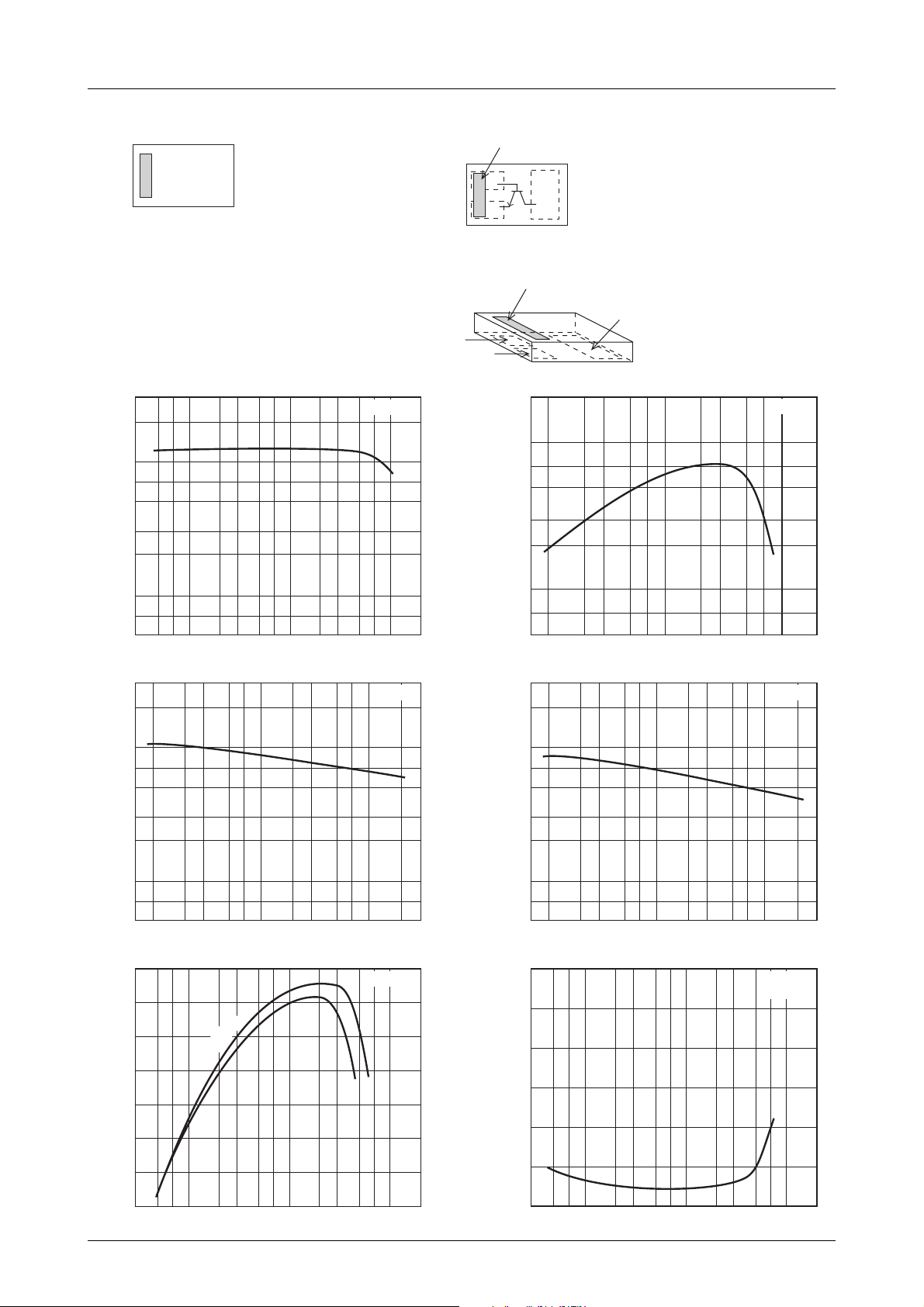
DC Current Gain, h
10
7
5
3
2
1.0
hFE -- I
32
Collector Current, IC–mA
Cob -- V
C
57 32257357
10 100
CB
VCE=5V
IT01363
f=1MHz
2
10
– GHz
7
T
5
3
2
1.0
Gain-Bandwidth Product, f
7
5
7223 5723 57
1.0
3
2
f
-- I
T
C
Collector Current, IC–mA
10 100
Cre -- V
CB
VCE=5V
IT01364
f=1MHz
1.0
7
5
3
2
Output Capacitance, Cob – pF
0.1
7
5
325
Collector-to-Base Voltage, VCB- - V Collector-to-Base Voltage, VCB-- V
14
12
–dB
2
10
8
6
4
2
Forward Transfer Gain, S21e
0
33257
S21e
=5V
CE
V
1.0
Collector Current, IC–mA
1.0
7
5
3
2
0.1
7
Reverse Transfer Capacitance, Cre – pF
73257 327
1.0
2
-- I
C
100.1
IT01365
f=1GHz
5
12
325
73257 327
1.0
NF -- I
100.1
IT01366
C
VCE=5V
f=1GHz
10
2V
8
6
4
Noise Figure, NF – dB
2
10
325757 2
100
IT01367
0
1.0
32
57 32257357
Collector Current, IC–mA
10 100
IT01368
No.6523–2/5
Page 3

P
-- Ta
120
100
C
– mW
80
C
60
40
20
Collector Dissipation, P
0
2006040 80 100 140120 160
Ambient Temperature, Ta – °C
S Parameters (Common emitter)
VCE=1V, IC=1mA, ZO=50Ω
EC3H02B
IT01369
)zHM(qerFS|11|
001559.06.22–814.33.361650.00.67579.05.01–
002229.00.34–901.37.841401.02.36129.06.91–
004548.02.77–716.28.421561.02.44497.09.23–
006287.08.101–651.27.701981.03.13496.05.14–
008647.01.911–887.12.49002.05.32036.07.74–
0001437.01.131–894.17.38102.07.71695.02.25–
0021717.02.141–623.16.47891.07.41375.06.75–
0041707.09.841–451.16.66391.00.21955.09.16–
0061807.05.551–920.12.06281.07.01165.01.66–
0081117.06.161–359.06.45171.08.01165.06.17–
0002217.05.661–088.03.94061.00.31965.05.67–
∠ S
11
S|12|
∠ S
12
S|21|
∠ S
21
VCE=1V, IC=5mA, ZO=50Ω
)zHM(qerFS|11|
001818.09.74–033.310.051940.03.46968.08.92–
002937.02.38–545.016.921670.06.94186.00.05–
004166.09.221–886.64.701890.08.73544.03.17–
006726.02.241–627.49.59601.04.53433.07.18–
008616.08.351–356.35.78411.03.63972.02.98–
0001416.08.161–989.27.08221.04.83252.07.49–
0021116.03.761–435.21.57031.08.04832.00.99–
0041706.02.271–702.21.07931.01.34132.08.201–
0061706.06.671–569.15.56941.01.54722.04.601–
0081016.08.971677.11.16951.01.74032.08.901–
0002906.09.671726.10.75171.06.84732.01.211–
∠ S
11
S|12|
∠ S
12
S|21|
∠ S
21
S|22|
S|22|
∠ S
∠ S
22
22
No.6523–3/5
Page 4

EC3H02B
VCE=2V, IC=3mA, ZO=50Ω
)zHM(qerFS|11|
001098.01.23–921.93.851240.01.27839.01.71–
002728.06.95–989.70.141370.06.75428.02.03–
004527.07.89–328.55.711401.08.14816.05.54–
006666.09.121–553.44.301511.05.43694.03.25–
008146.09.631–844.31.39121.02.23924.05.65–
0001136.03.741–458.21.58521.00.23293.09.95–
0021426.09.451–634.25.87821.01.33273.09.26–
0041816.03.161–421.28.27131.02.53063.00.66–
0061616.07.661–498.15.76431.06.73253.01.96–
0081816.04.171–517.17.26931.03.04153.09.27–
0002816.01.571–175.11.85441.02.34753.04.67–
∠ S
11
S|12|
VCE=2V, IC=10mA, ZO=50Ω
)zHM(qerFS|11|
001517.08.06–684.127.341530.01.26608.01.63–
002346.06.89–994.518.221150.02.94085.08.65–
004985.01.531–211.93.301560.08.44553.08.57–
006075.05.151–692.69.39570.03.74162.05.48–
008465.01.161–618.49.68780.09.05512.09.09–
0001365.07.761–129.31.18890.06.35291.04.59–
0021065.03.271–803.33.67211.00.65181.00.99–
0041855.02.671–768.21.27521.07.75271.06.201–
0061855.00.081055.21.86931.08.85961.03.501–
0081265.08.671392.22.46551.05.95071.08.701–
0002165.04.471290.25.06961.08.95671.02.901–
∠ S
11
S|12|
∠ S
∠ S
12
12
S|21|
S|21|
∠ S
∠ S
21
21
S|22|
S|22|
∠ S
∠ S
22
22
VCE=5V, IC=7mA, ZO=50Ω
)zHM(qerFS|11|
001797.09.24–036.710.251030.04.86298.03.22–
002807.01.67–071.414.231840.01.55327.07.63–
004806.00.611–681.94.011460.04.54494.09.84–
006565.04.631–435.69.89370.06.44583.05.25–
008055.08.841–550.58.09180.08.64923.00.45–
0001745.00.751–431.43.48980.09.94992.04.55–
0021145.02.361–794.30.97890.04.25582.07.65–
0041735.01.861–520.34.47901.00.55772.09.75–
0061935.05.271–786.20.07911.00.75072.01.06–
0081045.05.671–524.28.56031.06.85172.00.36–
0002045.04.971–212.29.16241.09.95772.08.56–
∠ S
11
S|12|
∠ S
12
S|21|
∠ S
21
S|22|
∠ S
22
No.6523–4/5
Page 5

VCE=5V, IC=20mA, ZO=50Ω
EC3H02B
)zHM(qerFS|11|
001816.05.17–252.031.831320.06.06847.00.73–
002455.05.011–113.027.711430.07.25115.09.25–
004915.01.341–914.115.001640.05.45603.06.26–
006705.08.651–018.74.29850.07.85032.00.46–
008405.00.561–149.52.68170.02.26391.09.46–
0001505.05.071–618.41.18480.07.46571.00.66–
0021405.03.471–150.48.67890.02.66761.00.76–
0041205.08.771–205.30.37211.02.76261.02.86–
0061405.09.871701.33.96721.04.76951.01.07–
0081805.00.671887.27.56241.04.76161.04.27–
0002705.09.371935.23.26551.01.76961.08.47–
∠ S
11
S|12|
∠ S
12
S|21|
∠ S
21
S|22|
∠ S
22
Specifications of any and all SANYO products described or contained herein stipulate the performance,
characteristics, and functions of the described products in the independent state, and are not guarantees
of the performance, characteristics, and functions of the described products as mounted in the customer's
products or equipment. To verify symptoms and states that cannot be evaluated in an independent device,
the customer should always evaluate and test devices mounted in the customer's products or equipment.
SANYO Electric Co., Ltd. strives to supply high-quality high-reliability products. However, any and all
semiconductor products fail with some probability. It is possible that these probabilistic failures could
give rise to accidents or events that could endanger human lives, that could give rise to smoke or fire,
or that could cause damage to other property. When designing equipment, adopt safety measures so
that these kinds of accidents or events cannot occur. Such measures include but are not limited to protective
circuits and error prevention circuits for safe design, redundant design, and structural design.
In the event that any or all SANYO products(including technical data,services) described or
contained herein are controlled under any of applicable local export control laws and regulations,
such products must not be exported without obtaining the export license from the authorities
concerned in accordance with the above law.
No part of this publication may be reproduced or transmitted in any form or by any means, electronic or
mechanical, including photocopying and recording, or any information storage or retrieval system,
or otherwise, without the prior written permission of SANYO Electric Co. , Ltd.
Any and all information described or contained herein are subject to change without notice due to
product/technology improvement, etc. When designing equipment, refer to the "Delivery Specification"
for the SANYO product that you intend to use.
Information (including circuit diagrams and circuit parameters) herein is for example only ; it is not
guaranteed for volume production. SANYO believes information herein is accurate and reliable, but
no guarantees are made or implied regarding its use or any infringements of intellectual property rights
or other rights of third parties.
This catalog provides information as of September, 2000. Specifications and information herein are
subject to change without notice.
PS No.6523–5/5
 Loading...