

Page 1
Ordering number : ENN6573
EC3H01B
NPN Epitaxial Planar Silicon Transistor
EC3H01B
VHF Band Low-Noise Amplifer
and OSC Applications
Features
•
Low noise : NF=1.8dB typ (f=150MHz).
• High gain : S21e
• Ultraminiature (1006 size) and thin (0.5mm) leadless
package.
2
=16dB typ (f=150MHz).
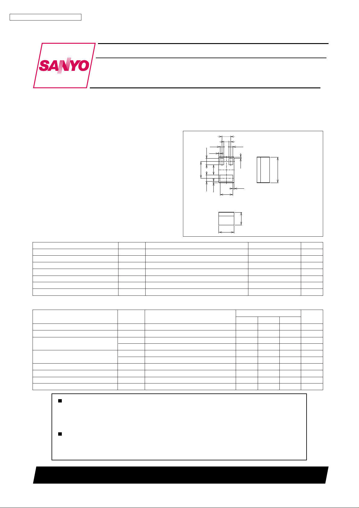
Package Dimensions
unit : mm
2183
0.25
0.65
0.25
0.35
0.15
0.05
1
0.4
0.05
(Bottom View)
0.2
3
0.5
[EC3H01B]
0.15
2
0.05
0.05
1.0
1 : Base
2 : Emitter
Specifications
0.5
0.6
Absolute Maximum Ratings at T a=25°C
Parameter Symbol Conditions Ratings Unit
Collector-to-Base Voltage V
Collector-to-Emitter Voltage V
Emitter-to-Base Voltage V
Collector Current I
Collector Dissipation P
Junction T emperature Tj 150 °C
Storage Temperature T stg --55 to +150 °C
CBO
CEO
EBO
C
C
3 : Collector
SANYO : E-CSP1006-3
20 V
12 V
2V
50 mA
100 mW
Electrical Characteristics at Ta=25°C
Parameter Symbol Conditions
Collector Cutoff Current I
Emitter Cutoff Current I
DC Current Gain
Gain Bandwidth Product
Output Capacitance Cob VCB=10V, f=1MHz 1.1 1.8 pF
Reverse Transfer Capacitance Cre VCB=10V, f=1MHz 0.8 pF
Forward Transfer Gain
Noise Figure NF VCE=2V, IC=3mA, f=150MHz 1.8 3.0 dB
CBO
EBO
hFE1VCE=2V, IC=3mA 100 180
hFE2VCE=2V, IC=50mA 70
fT1VCE=2V, IC=3mA 1.0 1.7 GHz
fT2VCE=2V, IC=20mA 5.0 GHz
S21e
VCB=10V, IE=0 1.0 µA
VEB=1V, IC=0 10 µA
2
VCE=2V, IC=3mA, f=150MHz 13 16 dB
Any and all SANYO products described or contained herein do not have specifications that can handle
applications that require extremely high levels of reliability, such as life-support systems, aircraft's
control systems, or other applications whose failure can be reasonably expected to result in serious
physical and/or material damage. Consult with your SANYO representative nearest you before using
any SANYO products described or contained herein in such applications.
SANYO assumes no responsibility for equipment failures that result from using products at values that
exceed, even momentarily, rated values (such as maximum ratings, operating condition ranges, or other
parameters) listed in products specifications of any and all SANYO products described or contained
herein.
Ratings
min typ max
SANYO Electric Co.,Ltd. Semiconductor Company
TOKYO OFFICE Tokyo Bldg., 1-10, 1 Chome, Ueno, Taito-ku, TOKYO, 110-8534 JAPAN
72100 TS IM TA-2481
No.6573-1/5
Unit
Page 2
EC3H01B
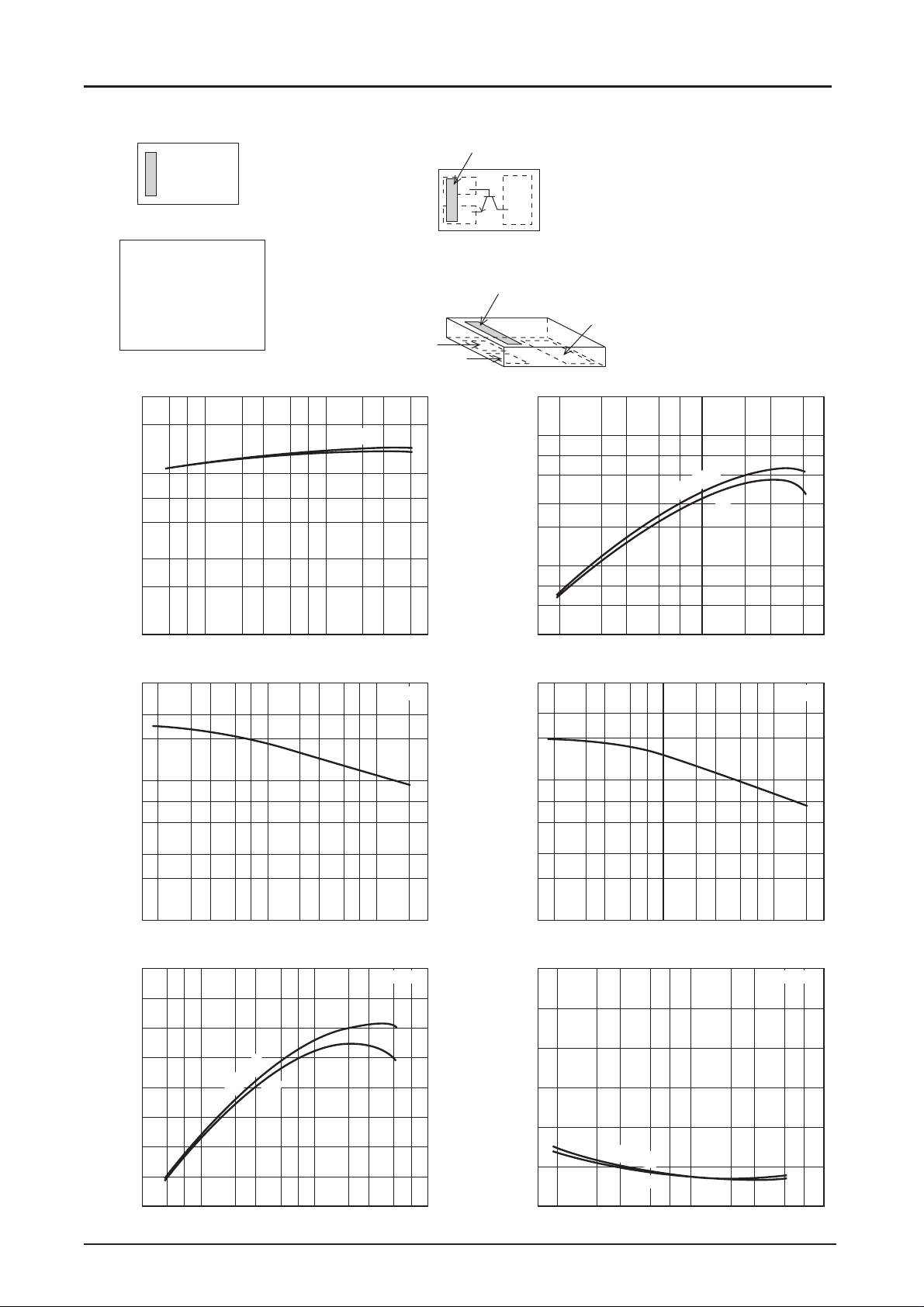
Type No. Indication (Top view) Electrical Connection (Top view)
Polarity mark (Top)
A
This product adopts a
high-frequency process.
Please be careful when
handling it beause it is
susceptible to static
electricity.
3
2
FE
100
7
5
3
DC Current Gain, h
2
10
5
3
2
1.0
Collector Current, IC -- mA
h
FE -- IC
23 577
Cob -- V
CB
VCE=2V
10
Base
Collector
Emitter
*Electrodes : on the bottom
Polarity mark (Top)
Collector
Base
Emitter
f
-- I
T
2
10
1V
23 5735
IT01305 IT01306
f=1MHz
7
-- GHz
T
5
3
2
1.0
7
5
Gain-Bandwidth Product, f
3
7
1.0 10
Collector Current, IC -- mA
5
3
2
Cre -- V
C
=2V
CE
V
1V
CB
23 5723 57
f=1MHz
2
Output Capacitance, Cob -- pF
-- dB
Forward Transfer Gain, S21e
1.0
0.1
1.0
7
5
3
2
7
5
3
2
Reverse Transfer Capacitance, Cre -- pF
0.1
7
32
28
24
20
23 57
0.1
Collector-to-Base Voltage, V
S21e2 -- I
1.0
23 2357
CB --
C
10
IT01307 IT01308
V
f=150MHz
7
0.1 1.0
12
10
dB
8
--
Collector-to-Base Voltage, V
NF -- I
23 235723 57
CB --
10
V
C
f=150MHz
=2V
16
12
8
4
0
57
1.0
CE
V
1V
233572357
Collector Current, IC -- mA
10 100
IT01309
6
4
Noise Figure, NF
2
0
7
1.0
V
=2V
CE
1V
2 3 57 2 3 57
Collector Current, IC -- mA
10 100
IT01310
No.6573-2/5
Page 3

EC3H01B
P
-- Ta
120
100
-- mW
80
C
60
40
20
Collector Dissipation, P
0
0 16014012010080604020
Ambient Temperature, Ta -- °C
S Parameters (Common emitter)
VCE=1V, IC=3mA, ZO=50Ω
Freq(MHz)
50 0.896 --43.1 9.814 154.6 0.054 66.4 0.909 --23.3
100 0.877 --72.4 7.271 137.7 0.095 51.7 0.794 --35.5
150 0.835 --99.6 6.387 123.3 0.109 38.1 0.630 --52.5
200 0.826 --112.9 5.162 114.2 0.123 31.8 0.554 --56.6
250 0.815 --125.5 4.496 106.5 0.131 26.3 0.496 --60.0
300 0.815 --132.6 3.849 100.9 0.136 22.6 0.455 --63.1
350 0.799 --141.8 3.350 96.2 0.134 19.7 0.405 --69.4
400 0.798 --146.3 3.034 92.1 0.136 17.4 0.396 --69.6
450 0.798 --150.9 2.547 88.8 0.130 17.3 0.348 --77.8
500 0.793 --155.4 2.464 85.2 0.136 14.9 0.362 --75.3
C
IT01311
S
11
∠S
S
11
21
∠S
S
21
12
∠S
S
12
22
∠S
22
VCE=1V, IC=30mA, ZO=50Ω
Freq(MHz)
S
11
∠S
S
11
21
∠S
S
21
12
∠S
S
12
22
50 0.708 --116.6 31.386 124.6 0.031 45.7 0.651 --89.1
100 0.753 --145.8 18.450 107.7 0.039 34.5 0.531 --123.5
150 0.764 --157.7 12.776 100.4 0.041 35.5 0.499 --140.9
200 0.768 --164.1 9.666 96.0 0.044 38.1 0.481 --150.0
250 0.772 --167.9 7.795 92.9 0.048 42.0 0.475 --156.2
300 0.775 --170.8 6.539 90.4 0.052 45.3 0.472 --160.3
350 0.773 --173.0 5.627 88.2 0.056 46.9 0.472 --163.2
400 0.774 --174.7 4.926 86.5 0.060 50.0 0.471 --165.6
450 0.776 --176.2 4.406 85.0 0.063 51.5 0.471 --168.1
500 0.775 --177.7 3.971 83.3 0.068 53.1 0.468 --169.1
VCE=2V, IC=1mA, ZO=50Ω
Freq(MHz)
S
11
∠S
S
11
21
∠S
S
21
12
∠S
S
12
22
50 0.960 --27.0 3.322 163.6 0.045 75.5 0.979 --8.0
100 0.958 --47.3 2.991 149.3 0.083 61.8 0.936 --14.7
150 0.923 --71.2 2.712 136.7 0.113 50.8 0.882 --20.5
200 0.919 --83.6 2.330 126.5 0.131 40.9 0.819 --25.4
250 0.904 --97.6 2.211 117.3 0.146 35.0 0.802 --27.2
300 0.902 --106.8 2.103 110.3 0.152 28.1 0.746 --31.3
350 0.879 --118.1 2.047 103.5 0.164 24.1 0.755 --32.0
400 0.876 --125.0 1.654 98.2 0.165 20.1 0.740 --33.9
450 0.868 --132.0 1.484 93.1 0.162 16.3 0.696 --37.1
500 0.860 --137.8 1.392 88.6 0.166 13.0 0.708 --38.3
∠S
∠S
22
22
No.6573-3/5
Page 4

EC3H01B
VCE=2V, IC=3mA, ZO=50Ω
Freq(MHz)
50 0.910 --36.5 10.051 157.6 0.043 70.8 0.932 --18.0
100 0.882 --66.6 7.542 142.0 0.075 55.9 0.841 --27.7
150 0.854 --90.0 6.850 128.0 0.090 41.8 0.692 --41.3
200 0.837 --105.9 5.632 118.7 0.104 36.0 0.617 --44.6
250 0.825 --118.8 4.990 110.8 0.111 29.8 0.564 --46.9
300 0.817 --128.1 4.298 105.0 0.116 25.9 0.520 --49.5
350 0.805 --136.5 3.779 100.0 0.115 23.9 0.470 --53.5
400 0.803 --142.0 3.437 95.9 0.119 21.2 0.457 --53.7
450 0.802 --146.2 2.879 92.6 0.113 19.9 0.401 --59.5
500 0.797 --151.0 2.810 88.9 0.117 18.0 0.418 --57.5
VCE=2V, IC=10mA, ZO=50Ω
Freq(MHz)
50 0.781 --63.1 22.825 146.1 0.036 59.1 0.825 --38.9
100 0.765 --102.5 17.041 125.6 0.053 44.0 0.617 --63.6
150 0.755 --124.3 12.823 113.8 0.060 37.9 0.481 --80.1
200 0.749 --137.4 10.134 106.3 0.065 33.3 0.400 --89.9
250 0.750 --146.2 8.276 101.2 0.067 31.3 0.347 --99.5
300 0.748 --152.4 7.003 97.3 0.068 31.5 0.313 --105.1
350 0.747 --157.1 6.126 93.7 0.071 33.2 0.293 --111.8
400 0.747 --160.7 5.337 91.3 0.072 32.7 0.274 --116.3
450 0.747 --163.4 4.806 88.7 0.076 33.3 0.262 --119.8
500 0.746 --166.2 4.305 86.5 0.076 35.7 0.256 --124.2
S
11
S
11
∠S
∠S
S
11
11
21
S
21
∠S
∠S
S
21
21
12
S
12
∠S
∠S
S
12
12
22
S
22
∠S
∠S
22
22
VCE=2V, IC=30mA, ZO=50Ω
Freq(MHz)
S
11
∠S
S
11
21
∠S
S
21
12
∠S
S
12
22
50 0.668 --99.9 37.088 131.5 0.026 51.3 0.685 --68.6
100 0.708 --135.5 23.026 112.8 0.035 40.7 0.503 --102.7
150 0.721 --149.9 16.197 104.2 0.038 40.0 0.432 --122.1
200 0.725 --158.1 12.372 99.0 0.041 42.1 0.399 --134.2
250 0.728 --163.0 10.017 95.5 0.045 43.8 0.383 --142.9
300 0.733 --166.7 8.389 92.6 0.047 44.7 0.375 --148.4
350 0.730 --169.1 7.243 90.3 0.051 49.8 0.370 --152.3
400 0.733 --171.3 6.353 88.5 0.055 53.0 0.367 --155.8
450 0.732 --173.1 5.675 86.6 0.058 53.0 0.362 --158.4
500 0.734 --175.0 5.115 85.0 0.062 53.8 0.361 --160.5
∠S
22
No.6573-4/5
Page 5

EC3H01B
Specifications of any and all SANYO products described or contained herein stipulate the performance,
characteristics, and functions of the described products in the independent state, and are not guarantees
of the performance, characteristics, and functions of the described products as mounted in the customer's
products or equipment. To verify symptoms and states that cannot be evaluated in an independent device,
the customer should always evaluate and test devices mounted in the customer's products or equipment.
SANYO Electric Co., Ltd. strives to supply high-quality high-reliability products. However, any and all
semiconductor products fail with some probability. It is possible that these probabilistic failures could
give rise to accidents or events that could endanger human lives, that could give rise to smoke or fire,
or that could cause damage to other property. When designing equipment, adopt safety measures so
that these kinds of accidents or events cannot occur. Such measures include but are not limited to protective
circuits and error prevention circuits for safe design, redundant design, and structural design.
In the event that any or all SANYO products(including technical data,services) described or
contained herein are controlled under any of applicable local export control laws and regulations,
such products must not be exported without obtaining the export license from the authorities
concerned in accordance with the above law.
No part of this publication may be reproduced or transmitted in any form or by any means, electronic or
mechanical, including photocopying and recording, or any information storage or retrieval system,
or otherwise, without the prior written permission of SANYO Electric Co. , Ltd.
Any and all information described or contained herein are subject to change without notice due to
product/technology improvement, etc. When designing equipment, refer to the "Delivery Specification"
for the SANYO product that you intend to use.
Information (including circuit diagrams and circuit parameters) herein is for example only ; it is not
guaranteed for volume production. SANYO believes information herein is accurate and reliable, but
no guarantees are made or implied regarding its use or any infringements of intellectual property rights
or other rights of third parties.
This catalog provides information as of July, 2000. Specifications and information herein are subject
to change without notice.
No.6573-5/5
PS
 Loading...