

Page 1
©2002 Teccor Electronics E5 - 1 http://www.teccor.com
Thyristor Product Catalog +1 972-580-7777
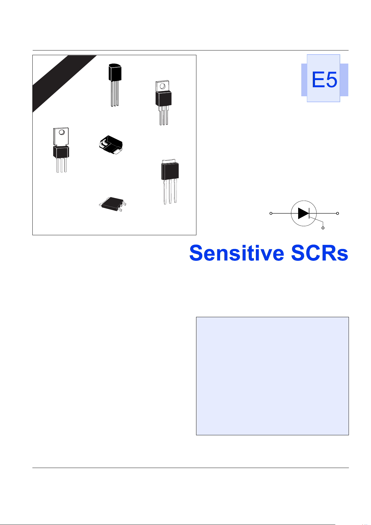
Selected Packages*
U.L. RECOGNIZED
File #E71639
(0.8 A to 10 A)
E5
General Description
The Teccor line of sensitive SCR semiconductors are half-wave
unidirectional, gate-controlled rectifiers (SCR-thyristor) which
complement Teccor's line of power SCRs. This group of
packages offers ratings of 0.8 A to 10 A, and 200 V to 600 V with
gate sensitivities of 12 µA to 500 µA. For gate currents in the
10 mA to 50 mA ranges, see “SCRs” section of this catalog.
The TO-220 and TO-92 are electrically isolated where the case
or tab is internally isolated to allow the use of low-cost assembly
and convenient packaging techniques.
Teccor's line of SCRs features glass-passivated junctions to
ensure long-term device reliability and parameter stability.
Teccor's glass offers a rugged, reliable barrier against junction
contamination.
Tape-and-reel packaging is available for the TO-92 package.
Consult the factory for more information.
Variations of devices covered in this data sheet are available for
custom design applications. Consult the factory for more
information.
Features
• Electrically-isolated TO-220 package
• High voltage capability — up to 600 V
• High surge capability — up to 100 A
• Glass-passivated chip
Compak Features
• Surface mount package — 0.8 A series
• New small-profile three-leaded Compak package
• Four gate sensitivities available
• Packaged in embossed carrier tape with 2,500
devices per reel
• Can replace SOT-223
TO-202
TO-92
3-lead
Compak
*TO-220
Isolated
TO-252
D-Pak
TO-251
V-Pak
AK
G
Page 2
Sensitive SCRs Data Sheets
http://www.teccor.com E5 - 2 ©2002 Teccor Electronics
+1 972-580-7777 Thyristor Product Catalog
See “General Notes” on page E5 - 4 and “Electrical Specifications Notes” on page E5 - 5
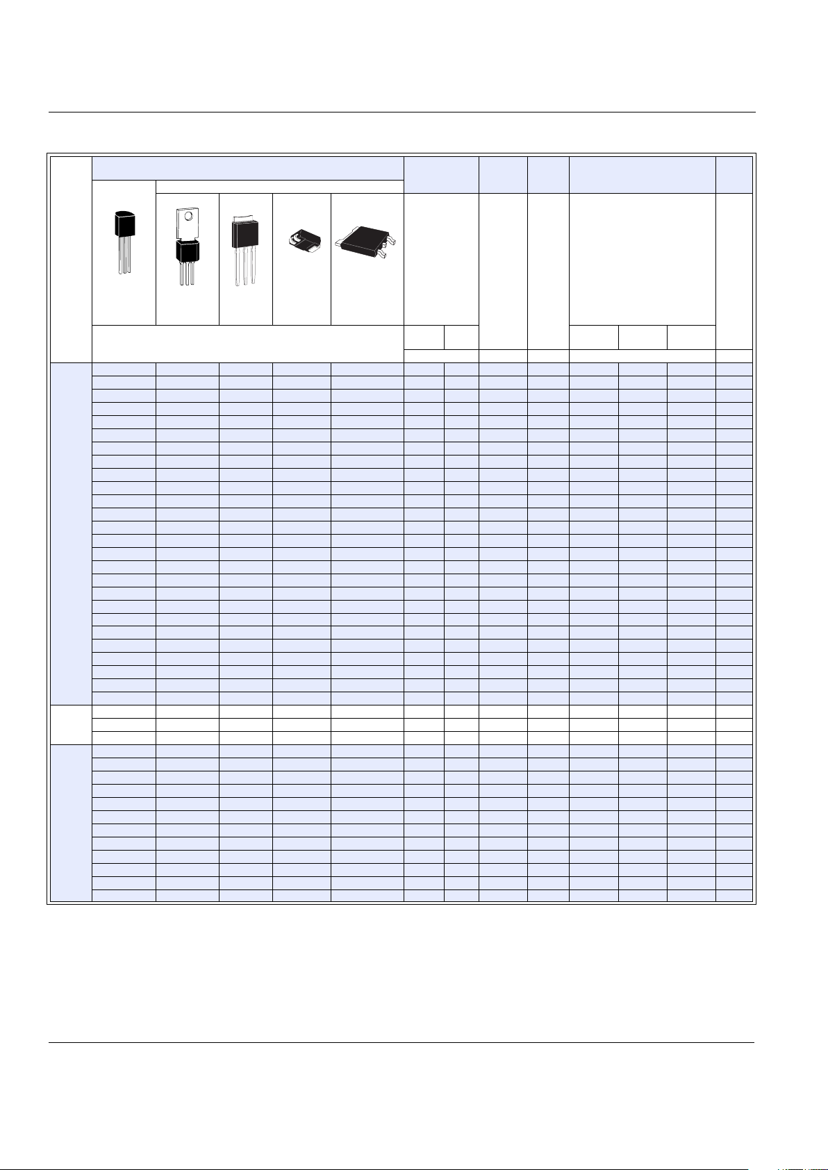
TYPE
Part Number
I
T
V
DRM
&
V
RRMIGT
I
DRM
&
I
RRM
V
TM
Non-isolated
TO-92
TO-202
TO-251
V-Pak Compa k
TO-252
D-Pak
(1)
Amps
Volts
(2) (12)
(14) (18)
µAmps
(20) (21)
µAmps
(3) (10)
Vol ts
See “Package Dimensions” section for variations. (11)
I
T(RMS)IT(AV)
TC or TL =
25 °C
TC or TL =
100 °C
TC or TL =
110 °C
MAX MIN MAX MAX MAX
0.8 A
S2S1 0.8 0.51 200 12 2 100 1.7
S4S1 0.8 0.51 400 12 2 100 1.7
S6S1 0.8 0.51 600 12 2 100 1.7
S2S2 0.8 0.51 200 50 2 100 1.7
S4S2 0.8 0.51 400 50 2 100 1.7
S6S2 0.8 0.51 600 50 2 100 1.7
S2S 0.8 0.51 200 200 2 100 1.7
S4S 0.8 0.51 400 200 2 100 1.7
S6S 0.8 0.51 600 200 2 100 1.7
S2S3 0.8 0.51 200 500 2 100 1.7
S4S3 0.8 0.51 400 500 2 100 1.7
S6S3 0.8 0.51 600 500 2 100 1.7
EC103B 0.8 0.51 200 200 1 50 1.7
EC103D 0.8 0.51 400 200 1 50 1.7
EC103M 0.8 0.51 600 200 2 100 1.7
EC103B1 0.8 0.51 200 12 1 50 1.7
EC103D1 0.8 0.51 400 12 1 50 1.7
EC103M1 0.8 0.51 600 12 2 100 1.7
EC103B2 0.8 0.51 200 50 1 50 1.7
EC103D2 0.8 0.51 400 50 1 50 1.7
EC103M2 0.8 0.51 600 50 2 100 1.7
EC103B3 0.8 0.51 200 500 1 50 1.7
EC103D3 0.8 0.51 400 500 1 50 1.7
EC103M3 0.8 0.51 600 500 2 100 1.7
2N5064 0.8 0.51 200 200 1 50 1.7
2N6565 0.8 0.51 400 200 1 100 1.7
1.5 A
TCR22-4 1.5 0.95 200 200 1 100 1.5
TCR22-6 1.5 0.95 400 200 1 100 1.5
TCR22-8 1.5 0.95 600 200 2 100 1.5
4A
T106B1 4 2.5 200 200 2 100 2.2
T106D1 4 2.5 400 200 2 100 2.2
T106M1 4 2.5 600 200 2 100 2.2
T107B1 4 2.5 200 500 2 100 2.5
T107D1 4 2.5 400 500 2 100 2.5
T107M1 4 2.5 600 500 2 100 2.5
S2004VS1 S2004DS1 4 2.5 200 50 2 100 1.6
S4004VS1 S4004DS1 4 2.5 400 50 2 100 1.6
S6004VS1 S6004DS1 4 2.5 600 50 2 100 1.6
S2004VS2 S2004DS2 4 2.5 200 200 2 100 1.6
S4004VS2 S4004DS2 4 2.5 400 200 2 100 1.6
S6004VS2 S6004DS2 4 2.5 600 200 2 100 1.6
K
G
A
K
A
G
A
A
A
G
K
A
G
K
A
A
K
G
Page 3
Data Sheets Sensitive SCRs
©2002 Teccor Electronics E5 - 3 http://www.teccor.com
Thyristor Product Catalog +1 972-580-7777
.
See “General Notes” on page E5 - 4 and “Electrical Specifications Notes” on page E5 - 5
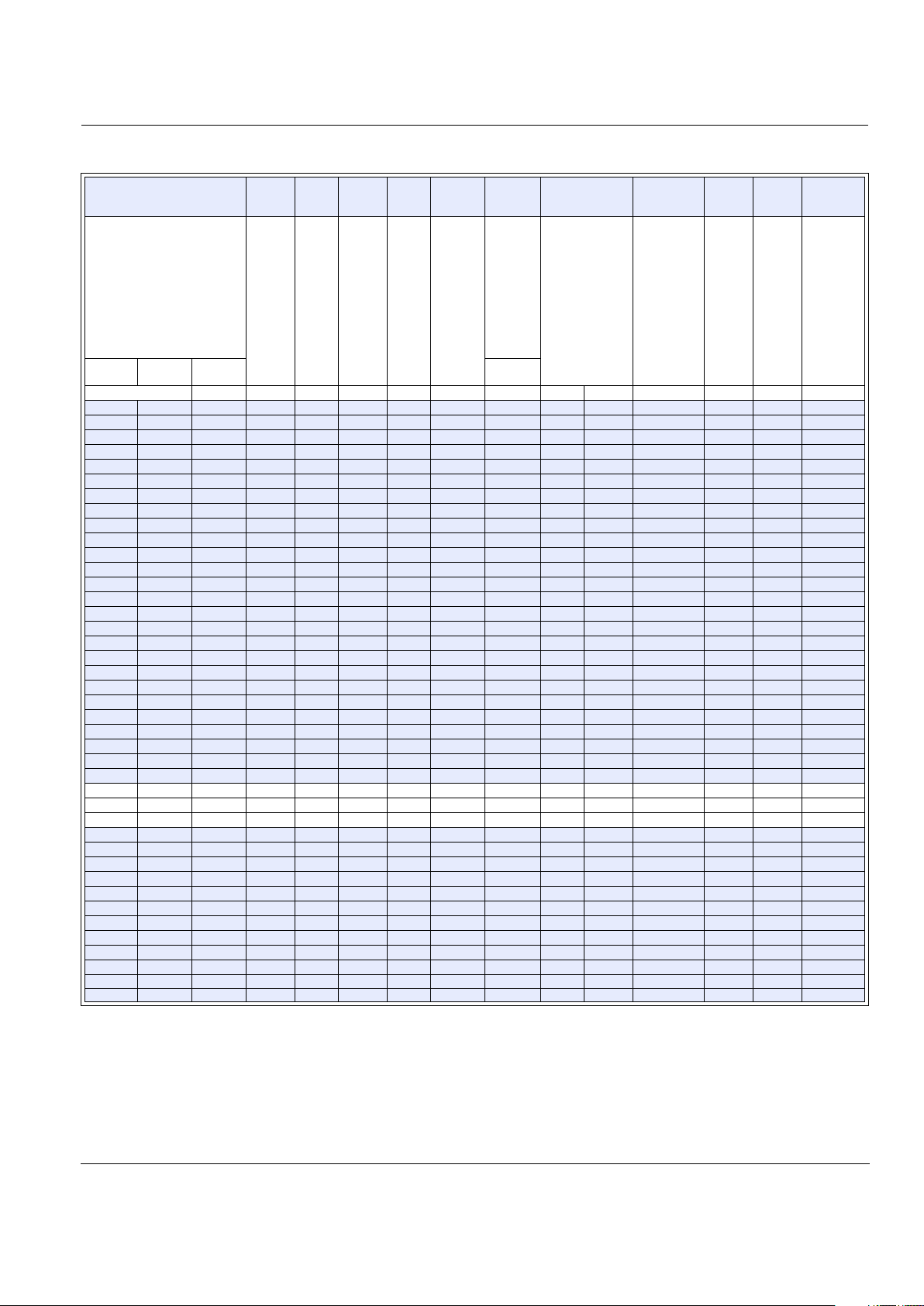
V
GT
I
H
I
GMVGRMPGM
P
G(AV)
I
TSM
dv/dt di/dt
t
gt
t
q
l2t
(4) (12) (22)
Volts
(5) (15)
(16) (19)
mAmps
(17)
Amps Volts
(17)
Watts Watts
(6) (7) (13)
Amps
Volts/µSec Amps/µSec
(8)
µSec
(9)
µSec Amps
2
/Sec
T
C
or TL =
-40 °C
TC or TL =
25 °C
TC or TL =
110 °C 60 /50 Hz
MAX MAX MIN MIN TYP (23) TYP MAX
1.2 0.8 0.2 5 1 5 1 0.1 20/16 20 50 2 60 1.6
1.2 0.8 0.2 5 1 5 1 0.1 20/16 20 50 2 60 1.6
1.2 0.8 0.2 5 1 5 1 0.1 20/16 10 50 2 60 1.6
1.2 0.8 0.25 5 1 5 1 0.1 20/16 25 50 3 60 1.6
1.2 0.8 0.25 5 1 5 1 0.1 20/16 25 50 3 60 1.6
1.2 0.8 0.25 5 1 5 1 0.1 20/16 10 50 3 60 1.6
1.2 0.8 0.25 5 1 5 1 0.1 20/16 30 50 4 50 1.6
1.2 0.8 0.25 5 1 5 1 0.1 20/16 30 50 4 50 1.6
1.2 0.8 0.25 5 1 5 1 0.1 20/16 15 50 4 50 1.6
1.2 0.8 0.25 8 1 5 1 0.1 20/16 40 50 5 45 1.6
1.2 0.8 0.25 8 1 5 1 0.1 20/16 40 50 5 45 1.6
1.2 0.8 0.25 8 1 5 1 0.1 20/16 20 50 5 45 1.6
1.2 0.8 0.25 5 1 5 1 0.1 20/16 30 50 3.5 50 1.6
1.2 0.8 0.25 5 1 5 1 0.1 20/16 30 50 3.5 50 1.6
1.2 0.8 0.25 5 1 5 1 0.1 20/16 15 50 3.5 50 1.6
1.2 0.8 0.2 5 1 5 1 0.1 20/16 20 50 2 60 1.6
1.2 0.8 0.2 5 1 5 1 0.1 20/16 20 50 2 60 1.6
1.2 0.8 0.2 5 1 5 1 0.1 20/16 10 50 2 60 1.6
1.2 0.8 0.25 5 1 5 1 0.1 20/16 25 50 3 60 1.6
1.2 0.8 0.25 5 1 5 1 0.1 20/16 25 50 3 60 1.6
1.2 0.8 0.25 5 1 5 1 0.1 20/16 10 50 3 60 1.6
1.2 0.8 0.25 8 1 5 1 0.1 20/16 40 50 5 45 1.6
1.2 0.8 0.25 8 1 5 1 0.1 20/16 40 50 5 45 1.6
1.2 0.8 0.25 8 1 5 1 0.1 20/16 20 50 5 45 1.6
1.2 0.8 0.25 5 1 5 1 0.1 20/16 25 50 2.2 60 1.6
1.2 0.8 0.25 5 1 6 1 0.1 20/16 25 50 2.2 60 1.6
1 0.80.2551610.120/1660 50 3.550 1.6
1 0.80.2551610.120/1640 50 3.550 1.6
1 0.80.2551610.120/1630 50 3.550 1.6
1 0.8 0.2 5 1 6 1 0.1 20/16 8 50 4 50 1.6
1 0.8 0.2 5 1 6 1 0.1 20/16 8 50 4 50 1.6
1 0.8 0.2 5 1 6 1 0.1 20/16 8 50 4 50 1.6
1 0.8 0.2 6 1 6 1 0.1 20/16 8 50 5 45 1.6
1 0.8 0.2 6 1 6 1 0.1 20/16 8 50 5 45 1.6
1 0.8 0.2 6 1 6 1 0.1 20/16 8 50 5 45 1.6
1 0.8 0.2 4 1 6 1 0.1 30/25 8 50 3 50 3.7
1 0.8 0.2 4 1 6 1 0.1 30/25 8 50 3 50 3.7
1 0.8 0.2 4 1 6 1 0.1 30/25 8 50 3 50 3.7
1 0.8 0.2 6 1 6 1 0.1 30/25 8 50 4 50 3.7
1 0.8 0.2 6 1 6 1 0.1 30/25 8 50 4 50 3.7
1 0.8 0.2 6 1 6 1 0.1 30/25 8 50 4 50 3.7
Page 4
Sensitive SCRs Data Sheets
http://www.teccor.com E5 - 4 ©2002 Teccor Electronics
+1 972-580-7777 Thyristor Product Catalog
Specific Test Conditions
di/dt — Maximum rate-of-change of on-state current; IGT = 50 mA pulse
width ³15 µsec with £0.1 µs rise time
dv/dt — Critical rate-of-rise of forward off-state voltage
I
2
t — RMS surge (non-repetitive) on-state current for period of 8.3 ms
for fusing
I
DRM
and I
RRM
— Peak off-state current at V
DRM
and V
RRM
IGT — DC gate trigger current VD = 6 V dc; RL = 100 W
I
GM
— Peak gate current
I
H
— DC holding current; initial on-state current = 20 mA
I
T
— Maximum on-state current
I
TSM
— Peak one-cycle forward surge current
P
G(AV)
— Average gate power dissipation
P
GM
— Peak gate power dissipation
t
gt
— Gate controlled turn-on time gate pulse = 10 mA; minimum
width = 15 µS with rise time £0.1 µs
t
q
— Circuit commutated turn-off time
V
DRM
and V
RRM
— Repetitive peak off-state forward and reverse voltage
V
GRM
— Peak reverse gate voltage
V
GT
— DC gate trigger voltage; VD = 6 V dc; RL = 100 W
V
TM
— Peak on-state voltage
General Notes
• Teccor 2N5064 and 2N6565 Series devices conform to all JEDEC
registered data. See specifications table on pages E5 - 2 and
E5 - 3.
• The case lead temperature (
T
C
or TL) is measured as shown on
dimensional outline drawings in the “Package Dimensions” section
of this catalog.
• All measurements (except I
GT
) are made with an external resistor
R
GK
= 1 kW unless otherwise noted.
• All measurements are made at 60 Hz with a resistive load at an
ambient temperature of +25 °C unless otherwise specified.
• Operating temperature (T
J
) is -65 °C to +110 °C for EC Series
devices, -65 °C to +125 °C for 2N Series devices, -40 °C to
+125 °C for “TCR” Series, and -40 °C to +110 °C for all others.
• Storage temperature range (T
S
) is -65 °C to +150 °C for TO-92
devices, -40 °C to +150 °C for TO-202 and Compak devices, and
-40 °C to +125 °C for all others.
• Lead solder temperature is a maximum of +230 °C for 10 seconds
maximum ³1/16" (1.59 mm) from case.
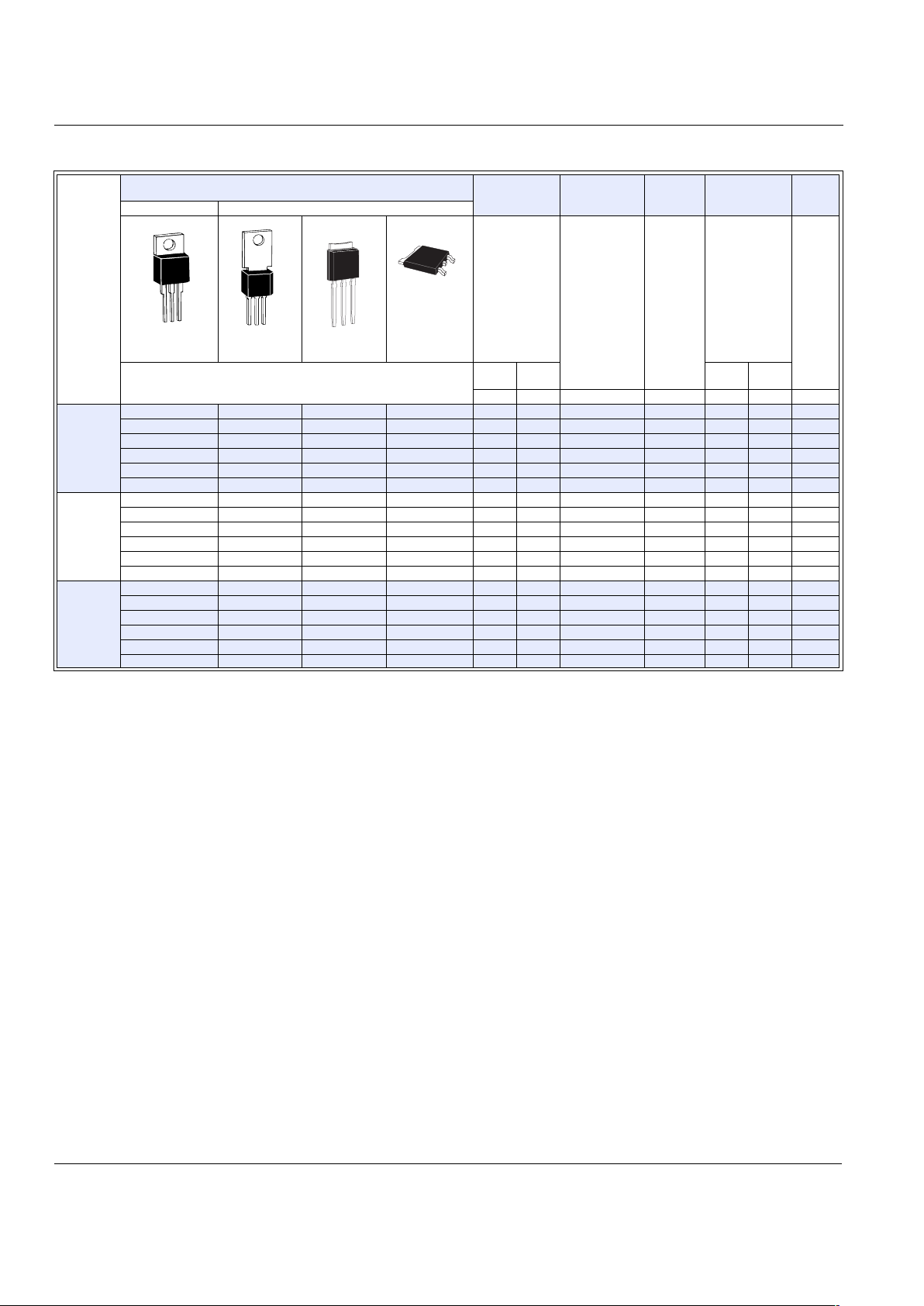
TYPE
Part Number
I
T
V
DRM
&
V
RRM
I
GT
I
DRM
&
I
RRM
V
TM
Isolated Non-isolated
TO-220 TO-202
TO-251
V-Pak
TO-252
D-Pak
(1)
Amps
Volts
(2) (12)
µAmps
(20) (21)
µAmps
(3) (10)
Vol ts
See “Package Dimensions” section for variations. (11)
I
T(RMS)IT(AV)
TC =
25 °C
TC =
110 °C
MAX MAX MIN MAX MAX MAX MAX
6A
S2006LS2 S2006FS21 S2006VS2 S2006DS2 6 3.8 200 200 5 250 1.6
S4006LS2 S4006FS21 S4006VS2 S4006DS2 6 3.8 400 200 5 250 1.6
S6006LS2 S6006FS21 S6006VS2 S6006DS2 6 3.8 600 200 5 250 1.6
S2006LS3 S2006FS31 S2006VS3 S2006DS3 6 3.8 200 500 5 250 1.6
S4006LS3 S4006FS31 S4006VS3 S4006DS3 6 3.8 400 500 5 250 1.6
S6006LS3 S6006FS31 S6006VS3 S6006DS3 6 3.8 600 500 5 250 1.6
8A
S2008LS2 S2008FS21 S2008VS2 S2008DS2 8 5.1 200 200 5 250 1.6
S4008LS2 S4008FS21 S4008VS2 S4008DS2 8 5.1 400 200 5 250 1.6
S6008LS2 S6008FS21 S6008VS2 S6008DS2 8 5.1 600 200 5 250 1.6
S2008LS3 S2008FS31 S2008VS3 S2008DS3 8 5.1 200 500 5 250 1.6
S4008LS3 S4008FS31 S4008VS3 S4008DS3 8 5.1 400 500 5 250 1.6
S6008LS3 S6008FS31 S6008VS3 S6008DS3 8 5.1 600 500 5 250 1.6
10 A
S2010LS2 S2010FS21 S2010VS2 S2010DS2 10 6.4 200 200 5 250 1.6
S4010LS2 S4010FS21 S4010VS2 S4010DS2 10 6.4 400 200 5 250 1.6
S6010LS2 S6010FS21 S6010VS2 S6010DS2 10 6.4 600 200 5 250 1.6
S2010LS3 S2010FS31 S2010VS3 S2010DS3 10 6.4 200 500 5 250 1.6
S4010LS3 S4010FS31 S4010VS3 S4010DS3 10 6.4 400 500 5 250 1.6
S6010LS3 S6010FS31 S6010VS3 S6010DS3 10 6.4 600 500 5 250 1.6
K
A
G
K
A
G
A
A
A
G
K
A
A
K
G
Page 5

Data Sheets Sensitive SCRs
©2002 Teccor Electronics E5 - 5 http://www.teccor.com
Thyristor Product Catalog +1 972-580-7777
Electrical Specifications Notes
(1) See Figure E5.1 through Figure E5.9 for current ratings at
specified operating temperatures.
(2) See Figure E5.10 for I
GT
versus TC or TL.
(3) See Figure E5.11 for instantaneous on-state current (i
T
) versus on-
state voltage (v
T
) TYP.
(4) See Figure E5.12 for V
GT
versus TC or TL.
(5) See Figure E5.13 for I
H
versus TC or TL.
(6) For more than one full cycle, see Figure E5.14.
(7) 0.8 A to 4 A devices also have a pulse peak forward current on-
state rating (repetitive) of 75 A. This rating applies for operation at
60 Hz, 75 °C maximum tab (or anode) lead temperature, switching
from 80 V peak, sinusoidal current pulse width of 10 µs minimum,
15 µs maximum. See Figure E5.20 and Figure E5.21.
(8) See Figure E5.15 for t
gt
versus IGT.
(9) Test conditions as follows:
– T
C
or T
L
£80 °C, rectangular current waveform
– Rate-of-rise of current £10 A/µs
– Rate-of-reversal of current £5A/µs
– I
TM
= 1 A (50 µs pulse), Repetition Rate = 60 pps
– V
RRM
= Rated
– V
R
= 15 V minimum, V
DRM
= Rated
– Rate-of-rise reapplied forward blocking voltage = 5 V/µs
– Gate Bias = 0 V, 100 W (during turn-off time interval)
(10) Test condition is maximum rated RMS current except TO-92
devices are 1.2 A
PK
; T106/T107 devices are 4 APK.
(11) See package outlines for lead form configurations. When ordering
special lead forming, add type number as suffix to part number.
(12) V
D
= 6 V dc, RL = 100 W (See Figure E5.19 for simple test circuit
for measuring gate trigger voltage and gate trigger current.)
(13) See Figure E5.1 through Figure E5.9 for maximum allowable case
temperature at maximum rated current.
(14) I
GT
= 500 µA maximum at TC = -40 °C for T106 devices
(15) I
H
= 10 mA maximum at TC = -65 °C for 2N5064 Series and
2N6565 Series devices
(16) I
H
= 6 mA maximum at TC = -40 °C for T106 devices
(17) Pulse Width £10 µs
(18) I
GT
= 350 µA maximum at TC = -65 °C for 2N5064 Series and
2N6565 Series devices
(19) Latching current can be higher than 20 mA for higher I
GT
types.
Also, latching current can be much higher at -40 °C. See Figure
E5.18.
(20) T
C
or TL = TJ for test conditions in off state
(21) I
DRM
and I
RRM
= 50 µA for 2N5064 and 100 µA for 2N6565 at
125 °C
(22) TO-92 devices specified at -65 °C instead of -40 °C
(23) T
C
= 110 °C
V
GT
I
H
I
GM
V
GRM
P
GM
P
G(AV)ITSM
dv/dt di/dt
t
gt
t
q
l2t
(4) (12) (22)
Volts
(5) (19)
mAmps
(17)
Amps Volts
(17)
Watts Watts
(6) (13)
Amps
Volts/ µSec
Amps/µSec
(8)
µSec
(9)
µSec Amps
2
Sec
T
C
=
-40 °C
TC =
25 °C
TC =
110 °C T
C
= 110 °C
MAX MAX MIN 60/50 Hz TYP TYP MAX
1 0.8 0.25 6 1 6 1 0.1 100/83 10 100 4 50 41
1 0.8 0.25 6 1 6 1 0.1 100/83 8 100 4 50 41
1 0.8 0.25 6 1 6 1 0.1 100/83 8 100 4 50 41
1 0.8 0.25 8 1 6 1 0.1 100/83 10 100 5 45 41
1 0.8 0.25 8 1 6 1 0.1 100/83 8 100 5 45 41
1 0.8 0.25 8 1 6 1 0.1 100/83 8 100 5 45 41
1 0.8 0.25 6 1 6 1 0.1 100/83 10 100 4 50 41
1 0.8 0.25 6 1 6 1 0.1 100/83 8 100 4 50 41
1 0.8 0.25 6 1 6 1 0.1 100/83 8 100 4 50 41
1 0.8 0.25 8 1 6 1 0.1 100/83 10 100 5 45 41
1 0.8 0.25 8 1 6 1 0.1 100/83 8 100 5 45 41
1 0.8 0.25 8 1 6 1 0.1 100/83 8 100 5 45 41
1 0.8 0.25 6 1 6 1 0.1 100/83 10 100 4 50 41
1 0.8 0.25 6 1 6 1 0.1 100/83 8 100 4 50 41
1 0.8 0.25 6 1 6 1 0.1 100/83 8 100 4 50 41
1 0.8 0.25 8 1 6 1 0.1 100/83 10 100 5 45 41
1 0.8 0.25 8 1 6 1 0.1 100/83 8 100 5 45 41
1 0.8 0.25 8 1 6 1 0.1 100/83 8 100 5 45 41
Page 6

Sensitive SCRs Data Sheets
http://www.teccor.com E5 - 6 ©2002 Teccor Electronics
+1 972-580-7777 Thyristor Product Catalog
*Mounted on 1 cm2 copper foil surface; two-ounce copper foil
Electrical Isolation
Teccor’s isolated sensitive SCRs will withstand a minimum high
potential test of 2500 V ac rms from leads to mounting tab over
the device's operating temperature range. The following table
shows other standard and optional isolation ratings.
*UL Recognized File #E71639
**For 4000 V isolation, use “V” suffix in part number.
Figure E5.1 Maximum Allowable Case Temperature versus
RMS On-state Current
Figure E5.2 Maximum Allowable Case Temperature versus
RMS On-state Current
Figure E5.3 Maximum Allowable Case Temperature versus
Average On-state Current
Thermal Resistance (Steady State)
R
qJC
[R
q JA
] °C/W (TYPICAL)
Package Code
ELF2FCDV
Typ e
TO-92 TO-220 TO-202
Type 2, 4, & 41
TO-202
Type 1 & 3
Compak TO-252
D-Pak
TO-251
V-Pak
0.8 A 75 [160] 60*
1.5 A 50 [160]
4.0 A 10 [100] 6.2 [80] 3.0 3.8 [85]
6.0 A 4.0 [65] 4.3 1.8 2.4
8.0 A 3.4 3.9 1.5 2.1
10.0 A 3.0 3.4 1.45 1.72
Electrical Isolation *
from Leads to Mounting Tab
V AC RMS TO-220
2500
Standard
4000
Optional **
50
60
70
80
90
100
110
120
130
CURRENT WAVEFORM: Sinusoidal
LOAD: Resistive or Inductive
CONDUCTION ANGLE: 180
˚
CASE TEMPERATURE: Measured
as Shown on Dimensional Drawing
RMS On-State Current [
I
T(RMS)
] – Amps
Maximum Allowable
Case Temperature (T
C
)
– ˚C
Compak
0.1 0.2 0.3 0.4 0.5 0.6 0.7 0.8 0.9 1.0
EC Series
JEDEC 2N Series
0 0.5 1.0 1.5 2.0 2.5 3.0 3.5 4.0
40
50
60
70
80
90
100
110
120
130
CURRENT WAVEFORM: Sinusoidal
LOAD: Resistive or Inductive
CONDUCTION ANGLE: 180˚
CASE TEMPERATURE: Measured
as Shown on Dimensional Drawing
RMS On-state Current [
I
T(RMS)
] – Amps
Maximum Allowable Case Temperature (
T
C
) – ˚C
2.6
4 A TO-251
and TO-252
T106 and T107
Type 1 and 3
T106 and T107
Type 2 and 4
TCR22 Devices
0 0.1 0.2 0.3 0.4 0.5 0.6
50
60
70
80
90
100
110
120
130
CURRENT WAVEFORM: Sinusoidal
LOAD: Resistive or Inductive
CONDUCTION ANGLE: 180˚
CASE TEMPERATURE: Measured
as Shown on Dimensional Drawing
Average On-state Current [
I
T(AV)
] – Amps
Maximum Allowable Case Temperature (
T
C
) – ˚C
0.51
Compak
EC Series
JEDEC 2N Series
Page 7

Data Sheets Sensitive SCRs
©2002 Teccor Electronics E5 - 7 http://www.teccor.com
Thyristor Product Catalog +1 972-580-7777
Figure E5.4 Maximum Allowable Case Temperature versus
Average On-state Current
Figure E5.5 Maximum Allowable Ambient Temperature versus
On-state Current
Figure E5.6 Maximum Allowable Ambient Temperature versus
RMS On-state Current
Figure E5.7 Maximum Allowable Ambient Temperature versus
Average On-state Current
Figure E5.8 Maximum Allowable Case Temperature versus
RMS On-state Current
Figure E5.9 Maximum Allowable Case Temperature versus
Average On-state Current
0 0.5 1.0 1.5 2.0 2.5 3.0
50
60
70
80
90
100
110
120
130
Average On-state Current [I
T(AV)
] – Amps
Maximum Allowable
Case Temperature (T
C
) – ˚C
0.95
40
CURRENT WAVEFORM: Sinusoidal
LOAD: Resistive or Inductive
CONDUCTION ANGLE: 180
˚
CASE TEMPERATURE: Measured
as Shown on Dimensional Drawing
1.65 1.9 2.54
T106 and T107
Type 1 and 3
T106 and T107
Type 2 and 4
TCR22
Devices
0 0.1 0.2 0.3 0.4 0.5 0.6 0.7 0.8 0.9
140
120
100
80
60
40
20
CURRENT WAVEFORM: Sinusoidal
LOAD: Resistive or Inductive
CONDUCTION ANGLE: 180
˚
FREE AIR RATING
1.5 A and JEDEC
2N Series I
T(AV)
and EC Series I
T(AV)
On-state Current – Amps
Maximum Allowable Ambient Temperature (T
A
) – ˚C
1.5 A Devices
and JEDEC
2N Series I
T(RMS)
EC Series I
T(RMS)
0 0.2 0.4 0.6 0.8 1.0 1.2 1.4 1.6 1.8
140
120
100
80
60
40
20
RMS On-state Current [I
T(RMS)
] – Amps
Maximum Allowable
Ambient Temperature (T
A
) – ˚C
2.0
CURRENT WAVEFORM: Sinusoidal
LOAD: Resistive or Inductive
CONDUCTION ANGLE: 180
˚
FREE AIR RATING
TO-220
T106/T107 TO-202
Type 1 and 3
T106/T107 TO-202
Type 2 and 4
and TO-251
0 0.2 0.4 0.6 0.8 1.0 1.2 1.4
20
40
60
80
100
120
140
CURRENT WAVEFORM: Sinusoidal
LOAD: Resistive or Inductive
CONDUCTION ANGLE: 180
˚
FREE AIR RATING
Average On-state Current [I
T(AV)
] – Amps
Maximum Allowable
Ambient Temperature (T
A
) – ˚C
TO-220
T106/T107 TO-202
Type 1 and 3
T106/T107 TO-202
Type 2 and 4
and TO-251
80
2468100
85
90
95
100
105
110
115
CURRENT WAVEFORM: Sinusoidal
LOAD: Resistive or Inductive
CONDUCTION ANGLE: 180
˚
TEMPERATURE: Measured as
Shown on Dimensional Drawings
RMS On-state Current [I
T(RMS)
] – Amps
Maximum Allowable
Case Temperature (T
C
) – ˚C
6 A TO-220
and TO-202
8 A TO-220
and TO-202
10 A TO-220
and TO-202
6 A TO-251
and TO-252
8 A TO-251
and TO-252
10 A TO-251
and TO-252
80
134560
85
90
95
100
105
110
Average On-state Current [I
T(AV)
] – Amps
Maximum Allowable
Case Temperature (T
C
) – ˚C
72
CURRENT WAVEFORM: Sinusoidal
LOAD: Resistive or Inductive
CONDUCTION ANGLE: 180
˚
CASE TEMPERATURE: Measured
as Shown on Dimensional Drawings
6 A TO-220
and TO-202
8 A TO-220
and TO-202
10 A TO-220
and TO-202
6 A TO-251
and TO-252
8 A TO-251
and TO-252
10 A TO-251
and TO-252
Page 8

Sensitive SCRs Data Sheets
http://www.teccor.com E5 - 8 ©2002 Teccor Electronics
+1 972-580-7777 Thyristor Product Catalog
Figure E5.10 Normalized DC Gate-Trigger Current versus
Case Temperature
Figure E5.11 Instantaneous On-state Current versus
On-state Voltage (Typical)
Figure E5.12 Normalized DC Gate-Trigger Voltage versus
Case Temperature
Figure E5.13 Normalized DC Holding Current versus Case Temperature
-65 -15 +25 +65 +110 +125-40
0
1.0
2.0
3.0
4.0
5.0
6.0
7.0
8.0
9.0
Case Temperature (TC) – ˚C
Ratio of
I
GT
I
GT
(T
C
= 25 ˚C)
See General Notes for specific device
operating temperature range.
0 .6 .8 1.0 1.2 1.4 1.6
0
4
8
12
16
20
24
28
32
TC = 25˚C
6 A to 10 A Devices
0.8 A to 1.5 A TO-92,
T106/T107, and
Compak
Instantaneous On-state Voltage (vT) – Volts
Instantaneous On-state Current (i
T
) – Amps
4 A TO-251 and TO-252
-65 -15 +25 +65 +110 +125-40
0
0.5
1.0
1.5
2.0
Case Temperature (TC) – ˚C
Ratio of
V
GT
V
GT
(
T
C
= 25
˚
C)
See General Notes for specific
operating temperature range
-65 -40 -15 +25 +65 +110 +125
0
1.0
2.0
3.0
4.0
See General Notes for specific
operating temperature range.
Case Temperature (TC) – ˚C
Ratio of
I
H
I
H
(T
C
= 25 ˚C)
Page 9

Data Sheets Sensitive SCRs
©2002 Teccor Electronics E5 - 9 http://www.teccor.com
Thyristor Product Catalog +1 972-580-7777
Figure E5.14 Peak Surge On-state Current versus Surge Current Duration
Figure E5.15 Typical Turn-on Time versus Gate Trigger Current
Figure E5.16 Power Dissipation (Typical) versus RMS On-state Current
1 2 3 4 5 6 8 10 20 30 40 50 60 80 100 200 300 400 600 100
0
1
2
3
4
5
6
8
10
20
30
40
50
60
80
100
200
SUPPLY FREQUENCY: 60 Hz Sinusoidal
LOAD: Resistive
RMS ON-STATE CURRENT: [I
T(RMS)
]: Max
Rated Value at Specified Case Temperature
Surge Current Duration – Full Cycles
Peak Surge (Non-repetitive)
On-state Current (I
TSM
) – Amps
Notes:
1) Gate control may be lost during
and immediately following surge
current interval.
2) Overload may not be repeated
until junction temperature has
returned to steady-state rated value.
6 A Devices
8 A Devices
10 A Devices
4 A TO-251 and TO-252
1.5 A Devices
TO-106
and TO-107
0.8 A TO-92
and Compak
0.01 0.1 1 10 100
0.1
1.0
10
100
IGT = 50 µA MAX
IGT = 200 µA MAX
IGT = 500 µA MAX
TC = 25 ˚C
IGT = 12 µA MAX
DC Gate Trigger Current (IGT) – mA
Turn-on Time (t
gt
) – µs
01234
1.0
2.0
3.0
4.0
5.0
T106 and T107
0.8 A TO-92 and Compak
1.5 A Devices
RMS On-state Current [I
T(RMS)
] – Amps
Average On-state Power Dissipation [P
D(AV)
] – Watts
CURRENT WAVEFORM: Half Sine Wave
LOAD: Resistive or Inductive
CONDUCTION ANGLE: 180˚
4 A TO-251 and TO-252
Page 10

Sensitive SCRs Data Sheets
http://www.teccor.com E5 - 10 ©2002 Teccor Electronics
+1 972-580-7777 Thyristor Product Catalog
Figure E5.17 Power Dissipation (Typical) versus RMS On-state Current
Figure E5.18 Normalized DC Latching Current versus Case Temperature
Figure E5.19 Simple Test Circuit for Gate Trigger Voltage and
Current Measurement
Note: V1 — 0 V to 10 V dc meter
V
GT
— 0 V to 1 V dc meter
I
G
— 0 mA to 1 mA dc milliammeter
R1 — 1 k potentiometer
To measure gate trigger voltage and current, raise gate voltage
(V
GT
) until meter reading V1 drops from 6 V to 1 V. Gate trigger
voltage is the reading on V
GT
just prior to V1 dropping. Gate trig-
ger current I
GT
can be computed from the relationship
where I
G
is reading (in amperes) on meter just prior to V1 drop-
ping.
Note: I
GT
may turn out to be a negative quantity (trigger current
flows out from gate lead).
024681
0
0
2
4
6
8
10
12
RMS On-state Current [I
T(RMS)
] – Amps
CURRENT WAVEFORM: Half Sine Wave
LOAD: Resistive or Inductive
CONDUCTION ANGLE: 180˚
Average On-state
Power Dissipation [P
D(AV)
] – Watts
6 A to 10 A
TO-220, TO-202,
TO-251, and TO-252
-65 -15 +25 +65 +110 +125-40
0
1.0
2.0
3.0
4.0
5.0
6.0
7.0
8.0
9.0
Case Temperature (TC) – ˚C
Ratio of
I
L
I
L
(
T
C
= 25 ˚C)
See General Notes for specific device
operating temperature range.
V1
6 V
DC
+
–
100
D.U.T.
Reset
Normally-closed
Pushbutton
1 k
(1%)
I
G
V
GT
100
I
GT
R1
IN4001
I
GTIG
V
GT
1000
-------------
Amps–=
Page 11

Data Sheets Sensitive SCRs
©2002 Teccor Electronics E5 - 11 http://www.teccor.com
Thyristor Product Catalog +1 972-580-7777
Figure E5.20 Peak Repetitive Capacitor Discharge Current
Figure E5.21 Peak Repetitive Sinusoidal Curve
180
160
140
120
100
80
60
40
20
0
1.0 3.0
5.0
7.0
10 30
50
70
100
Peak Discharge Current (I
TM
) – Amps
Peak Current Duration (tW) – µs
0.8 A to 4 A
I
TM
t
W
tW = 5 TIME CONSTANTS
60 Hz
12 Hz
1 Hz
180
160
140
120
100
80
60
40
20
0
1.0 3.0
5.0
7.0
10 30
50
70
100
Peak Discharge Current (I
TM
) – Amps
Peak Current Duration (tW) – µs
0.8 A to 4 A
I
TM
t
W
60 Hz
12 Hz
1 Hz
Page 12

Notes
 Loading...