

Datasheet E28F016SV-120, E28F016SV-080, E28F016SV-075, E28F016SV-070, E28F016SV-065 Datasheet (Intel Corporation)
...Page 1

E
28F016SV
16-MBIT (1 MBIT x 16, 2 MBIT x 8)
FlashFile™ MEMORY
Includes Commercial and Extended Temperature Specifications
n
SmartVoltage Technology
User-Selectable 3.3V or 5V V
User-Selectable 5V or 12V V
n
65 ns Access Time
n
1 Million Erase Cycles per Block
n
30.8 MB/sec Burst Write Transfer Rate
n
0.48 MB/sec Sustainable Write Transfer
Rate
n
Configurable x8 or x16 Operation
n
56-Lead TSOP and SSOP Type I
Packages
Intel’s 28F016SV 16-Mbit Flas hFile™ memory is a revolutionary architect ure which is the ideal choice for
designing embedded direct-execute c ode and mass s torage data/fi le flash m emory sys tems. Wi th innovati ve
capabilities, low-power operation, user-selectable V
28F016SV enables the design of trul y mobile, high-performance personal computing and communic ations
products.
The 28F016SV is the highest dens ity, highest performanc e nonvolatile read/program s olution for solid-s tate
storage applications. I ts s ymm etric ally-block ed architec ture (100% c ompat ible with the 28F008SA 8-Mbit and
28F016SA 16-Mbit FlashFile memories), extended cycling, flexible V
technology), fast program and read performance and select i ve block locking, provi de a highly-flexible memory
component suitable f or Resident Flash Arrays, high-density mem ory cards and PCMCIA-ATA flas h drives.
The 28F016SV’s dual read voltage enables t he design of memory cards which can be read/written in 3.3V
and 5V systems interchangeably. Its x8/x16 architecture allows optimization of the memory-to-processor
interface. The flexible block locking option enables bundling of executable application sof tware in a Resident
Flash Array or memory card. The 28F016SV is manufactured on Intel’s 0.6 µm ETOX IV process technology.
CC
PP
n
Backwards-Compatible with 28F016SA,
28F008SA Command Set
n
Revolutionary Architecture
Multiple Command Execution
Program during Erase
Command Super-Set of the Intel
28F008SA
Page Buffer Program
n
2 µA Typical Deep Power-Down
n
32 Independently Lockable Blocks
n
State-of-the-Art 0.6 µm ETOX™ IV Flash
Technology
voltage and high read/program performance, the
PP
and VPP voltage (SmartVoltage
CC
July 1997 Order Number: 290528-007
7/11/97 11:03 AM 29052807.DOC
Page 2

Information in this document is provided in connection with Intel products. No license, express or implied, by estoppel or
otherwise, to any intellectual property rights is granted by this document. Except as provided in Intel’s Terms and Conditi ons of
Sale for such products, Intel assumes no liability whatsoever, and Intel disclaims any express or implied warranty, relating to
sale and/or use of Intel products including liability or warranties relating to fitness for a particular purpose, merchantability, or
infringement of any patent, copyright or other intellectual property right. Intel products are not intended for use in medical, life
saving, or life sustaining applications.
Intel may make changes to specifications and product descriptions at any time, without notice.
The 28F016SV may contain design defects or errors known as errata which may cause the product to deviate from published
specifications. Current characterized errata are available on request.
Contact your local Intel sales office or your distributor to obtain the latest specifications and before placing your product order.
Copies of documents which have an ordering number and are referenced in this document, or other Intel literature, may be
obtained from:
Intel Corporation
P.O. Box 7641
Mt. Prospect, IL 60056-7641
or call 1-800-879-4683
or visit Intel’s Website at http:\\www.intel.com
COPYRIGHT © INTEL CORPORATION, 1997 CG-041493
*Third-party brands and names are the property of their respective owners.
Page 3

E 28F016SV FlashFile™ MEMORY
CONTENTS
PAGE PAGE
1.0 INTRODUCTION .............................................7
1.1 Enhanced Features......................................7
1.2 Product Overview.........................................7
2.0 DEVICE PINOUT.............................................9
2.1 Lead Descriptions ......................................11
3.0 MEMORY MAPS...........................................15
3.1 Extended Status Registers Memory Map...16
4.0 BUS OPERATIONS, COMMANDS AND
STATUS REGISTER DEFINITIONS................17
4.1 Bus Operations for Word-Wide Mode
(BYTE# = V
4.2 Bus Operations for Byte-Wide Mode
(BYTE# = V
4.3 28F008SA—Compatible Mode Command
Bus Definitions.............................................18
4.4 28F016SV—Performance Enhancement
Command Bus Definitions............................19
4.5 Compatible Status Register........................21
4.6 Global Status Register...............................22
4.7 Block Status Register.................................23
4.8 Device Configuration Code.........................24
)..............................................17
IH
)...............................................17
IL
5.0 ELECTRICAL SPECIFICATIONS..................25
5.1 Absolute Maximum Ratings........................25
5.2 Capacitance...............................................26
5.3 DC Characteristics (V
5.4 DC Characteristics (V
5V ± 0.25V)..................................................33
5.5 Timing Nomenclature .................................37
5.6 AC Characteristics—Read Only Operations38
5.7 Power-Up and Reset Timings.....................43
5.8 AC Characteristics for WE#—Controlled
Command Write Operations.........................44
5.9 AC Characteristics for CE#—Controlled
Command Write Operations)........................49
5.10 AC Characteristics for WE#—Controlled
Page Buffer Program Operations..................54
5.11 AC Characteristics for CE#—Controlled
Page Buffer Program Operations..................56
5.12 Erase and Word/Byte Program
Performance.................................................58
6.0 MECHANICAL SPECIFICATIONS.................60
APPENDIX A: Device Nomenclature and
Ordering Information .....................................61
APPENDIX B: Ordering Information .................63
= 3.3V ± 0.3V) .....29
CC
= 5V ± 0.5V)
CC
3
Page 4

28F016SV FlashFile™ MEMORY E
WHRH1A
WHRH1B
WHRH2
REVISION HISTORY
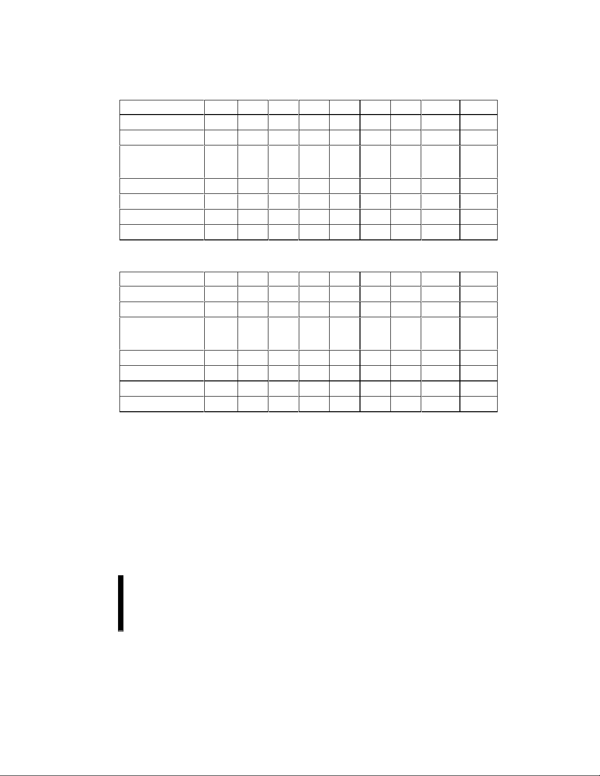
Number Description
-001
-002
-003
Original Version
Added 28F016SV-065/-070 at 5V V
and 28F016SV-075 at 3.3V VCC.
CC
Improved burst write transfer rate to 30.8 MB/sec.
Added 56-lead SSOP Type I packaging information.
Changed V
Increased I
I
CCR1
I
CCR2
I
CCR1
I
CCR2
from 2V to 1.5V.
PPLK
at 5V V
CCR
from 30 mA (typ)/35 mA (max) to 40 mA (typ)/50 mA (max) @ V
from 15 mA (typ)/20 mA (max) to 20 mA (typ)/30 mA (max) @ V
from 50 mA (typ)/60 mA (max) to 75 mA (typ)/95 mA (max) @ V
and 3.3V VCC:
= 3.3V
= 3.3V
= 5V
from 30 mA (typ)/35 mA (max) to 45 mA (typ)/55 mA (max) @ VCC = 5V
Moved AC Characteristics for Extended Register Reads into separate table.
Increased V
MAX from 13V to 14V.
PP
Added Erase Suspend Command Latency times to Section 5.12
Modified Device Nomenclature Section to include SSOP package option and Ordering
Information
Changed definition of “NC.” Removed “No internal connection to die” from description.
xx” to Upper Byte of Command (Data) Definition in Sections 4.3 and 4.4.
Added “
Added Note to Sleep Command (Section 4.4) denoting that the chip must be de-selected
in order for the power consumption in sleep mode to reach deep power-down
levels.
Modified parameters “V” and “I” of Section 5.1 to apply to “NC” pins.
Increased I
Changed V
(VPP Read Current) for VPP> VCC to 200 µA at VCC = 3.3V and VCC = 5V
PPR
= 5V DC Characteristics (Section 5.5) marked with Note 1 to indicate
that these currents are specified for a CMOS rise/fall time (10% to 90%) of <5 ns
and a TTL rise/fall time of <10 ns.
Corrected the graphical representation of t
WHGL
and t
in Figures 15 and 16.
EHGL
Increased Typical “Page Buffer Byte/Word Program Times” from 6.0 µs to 8.0 µs (Byte)
and 12.1 µs to 16.0 µs (Word) @ V
Increased Typ. “Byte/Word Program Times” (t
= 3.3V/5V and VPP = 5V:
CC
/t
WHRH1B
) for V
= 5V (Section
5.12)
t
from 16.5 µs to 29.0 µs and t
WHRH1A
t
from 11.0 µs to 20.0 µs and t
WHRH1A
Increased Typical “Block Program Times” (t
t
from 1.1 sec to 1.9 sec and t
WHRH2
t
from 0.8 sec to 1.4 sec and t
WHRH2
from 24.0 µs to 35.0 µs at V
from 16.0 µs to 25.0 µs at VCC = 5V
WHRH1B
WHRH3
WHRH3
/t
)for V
WHRH3
=5V (Section 5.12):
from 0.8 sec to 1.2 sec at V
from 0.6 sec to 0.85 sec at VCC = 5V
=3.3V
= 3.3V
Changed “Time from Erase Suspend Command to WSM Ready” spec name to “Erase
Suspend Latency Time to Read;” modified typical values and added Min/Max
values at V
=3.3/5V and VPP =5V/12V (Section 5.12)
CC
Added “Erase Suspend Latency Time to Program” Specifications to Section 5.12
Minor cosmetic changes throughout document
4
Page 5
E 28F016SV FlashFile™ MEMORY
)
REVISION HISTORY (Continued)
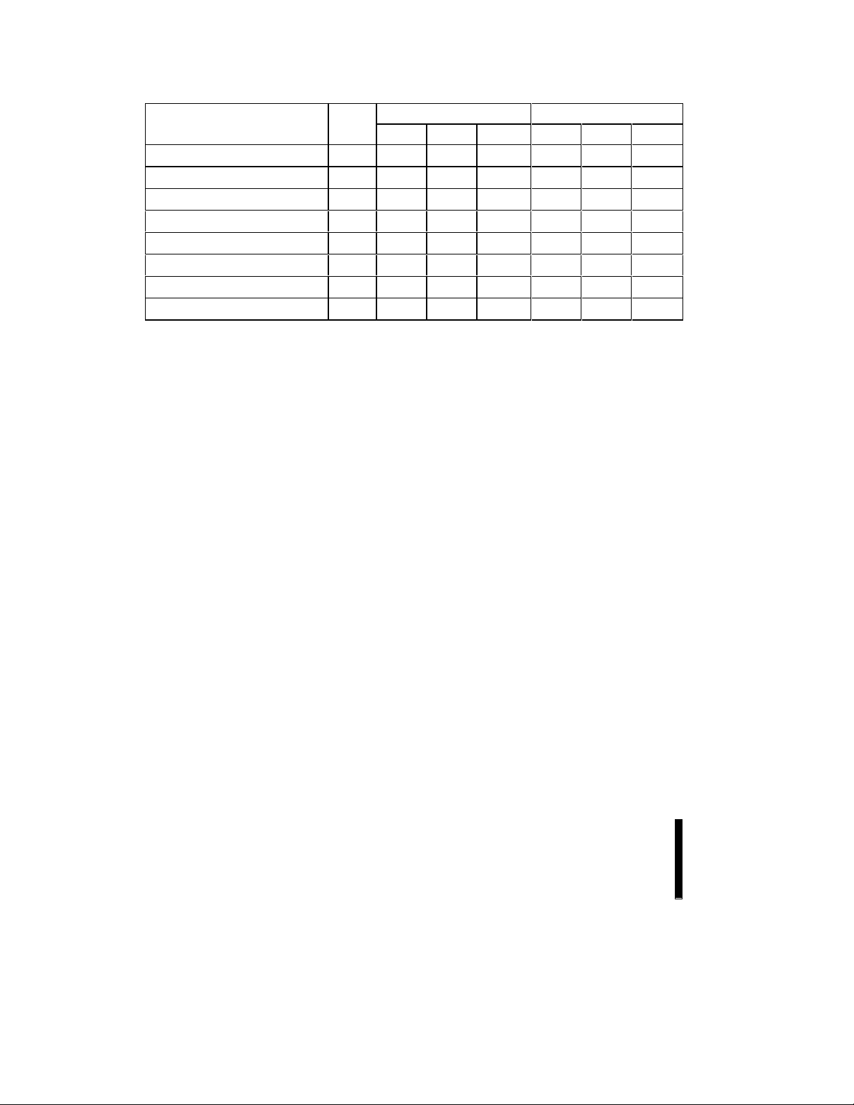
Number Description
-004 Added 3/5# pin to Block Diagram (Figure 1), Pinout Configurations (Figures 2 and 3),
Product Overview (Section 1.1) and Lead Descriptions (Section 2.1)
PLYL
PPES
CCS
, t
Specifications
, t
PLYH
, and t
YLPH
from 0.50 mm to 0.050 mm (Section 6.0)
1
, t
AVAV
ELWL
, t
AVAV
, t
AVAV
AVQV
)
ELEH
AVQV
YHPH
, t
specifications
, t
, and t
ELQV
)
EHEL
, t
, and t
ELQV
FLQV/tFHQV
FLQV/tFHQV)
5VPH
Added 3/5# pin to Test Conditions of I
Added 3/5# pin (Y) to Timing Nomenclature (Section 5.5)
Increased t
and 480 ns for E28F106SV 070 devices.
Modified Power-Up and Reset Timings (Section 5.9) to include 3/5# pin: Removed t
and t
Added t
Corrected TSOP Mechanical Specification A
Corrected SSOP Mechanical Spec. B (max) from 0.20 mm to 0.40 mm (Section 6.0)
Minor cosmetic changes throughout document.
-005 Updated DC Specifications: I
Updated AC Specifications: Page Buffer Reads: (t
Page Buffer WE#-Controlled Command Writes (t
CE#-Controlled Command Write Parameters (t
Combined Commercial and Extended Temperature information into single datasheet.
-006 Updated AC Specifications: Page Buffer Reads: (t
-007 Updated Disclaimer
Specifications at 5V VCC to 400 ns for E28F016SV 065 devices
PHQV
specifications; Added t
3VPH
PHEL3
and t
specifications to Power-Up and Reset Timings (Section 5.9)
PHEL5
, I
CCD
5
Page 6

28F016SV FlashFile™ MEMORY E
Page intentionally left blank
6
Page 7

E 28F016SV FlashFile™ MEMORY
1.0 INTRODUCTION
The documentation of t he Intel 28F016SV m em ory
device includes this datasheet, a detailed user’s
manual, and a number of application notes and
design tools, all of which are referenced in
Appendix B.
The datasheet is intended to give an overview of
the chip feature-set and of the operating AC/DC
specifications. The
User’s Manual
the user modes, system interface examples and
detailed descriptions of all principles of operation.
It also contains the full list of software algorithm
flowcharts, and a brief section on compatibility
with the Intel 28F008SA.
A significant 28F016SV change occurred between
datasheet revisions 290528-003 and 290528-004.
This change centers around the addit ion of a 3/5#
pin to the device’s pinout configuration. Figures 2
and 3 show the 3/5# pin assignment for TSOP and
SSOP Type 1 packages. I ntel recommends that all
customers obtain the latest revisi ons of 28F016SV
documentation.
16-Mbit Flash Product Family
provides complete descriptions of
1.1 Enhanced Features
The 28F016SV is backwards compatible with t he
28F016SA and offers the following enhancements:
• SmartVoltage Technology
Selectable 5V or 12V V
• VPP Level Bit in Block Status Register
• Additional RY/BY# Configuration
Pulse-On-Program/Erase
• Additional Upload Device Information
Command Feedback
Device Proliferation Code
Device Configuration Code
PP
1.2 Product Overview
The 28F016SV is a high-performance, 16-Mbit
(16,777,216-bit) block erasable, nonvolatile
random access memory, organized as either
1 Mword x 16 or 2 Mbyte x 8. The 28F016SV
includes thirty-two 64-KB (65,536 by te) blocks or
thirty-two 32-KW (32,768 word) blocks. A chip
memory map is shown in Figure 4.
The implementation of a new architecture, with
many enhanced features, will improve the device
operating characteristics and result in greater
product reliability and ease-of-use.
The 28F016SV incorporates SmartVoltage
technology, providing V
and 5V and program and erase capability at V
12V or 5V. Operating at V
28F016SV consumes approximately one half the
power consumption at 5V V
provides the highest read performance capability.
V
= 5V operation eliminates the need for a
PP
separate 12V converter, while V
maximizes program/erase performance. In
addition to the flexible program and erase
voltages, the dedicat ed V
protection with V
A 3/5# input pin configures the device’s internal
circuitry for optimal 3.3V or 5V read/program
operation.
A Command User Interface (CUI) serves as the
system interface between the microprocessor or
microcontroller and the internal memory operation.
Internal Algorithm Automation allows byte/word
programs and block erase operations to be
executed using a Two-Program command
sequence to the CUI in the same way as the
28F008SA 8-Mbit FlashFile™ memory.
A super-set of commands has been added to the
basic 28F008SA command-set to achieve higher
program performance and provide additional
capabilities. These new commands and features
include:
• Page Buffer Programs to Flash
• Command Queuing Capability
• Automatic Data Programs during Erase
• Software Locking of Memory Blocks
• Two-Byte Successive Programs in 8-bit
Systems
• Erase All Unlocked Blocks
Writing of memory data is performed in either byt e
or word increments typically within 6 µs
(12V V
28F008SA. A block erase operat ion erases one of
the 32 blocks in typically 0.6 sec (12V V
independent of the other blocks, which is about a
65% improvement over the 28F008SA.
PP
≤ V
PP
)—a 33% improvement over the
operation at both 3.3V
CC
= 3.3V, the
CC
, while 5V V
CC
PP
gives complete code
PP
.
PPLK
PP
CC
= 12V
PP
=
),
7
Page 8

28F016SV FlashFile™ MEMORY E
Each block can be writt en and erased a minimum
of 100,000 cycles. Systems can achieve one
million Block Erase Cycles by providing wearleveling algorithms and gracef ul block retirement.
These techniques have already been employ ed in
many flash file systems and hard disk drive
designs.
The 28F016SV incorporates two Page Buffers of
256 bytes (128 words) each to allow page data
programs. This feature can improve a system
program performance by up to 4.8 times over
previous flash memory devices, which have no
Page Buffers.
All operations are started by a sequence of
Program commands to the device. Three Status
Registers (described in detail later in this
datasheet) and a RY/BY# output pin provide
information on the progress of the requested
operation.
While the 28F008SA requires an operation to
complete before the next operation can be
requested, the 28F016SV allows queuing of the
next operation while the memory executes the
current operation. This eliminates system
overhead when writing several bytes in a row to
the array or erasing several blocks at the same
time. The 28F016SV can also perform program
operations to one block of memory while
performing erase of another block.
The 28F016SV provides selectable block locking
to protect code or data such as Device Drivers,
PCMCIA card information, ROM-Executable O/S
or Application Code. Each block has an
associated nonvolatile lock-bit which determines
the lock status of the block. In addition, the
28F016SV has a master Write Protect pi n (WP#)
which prevents any modifications to memory
blocks whose lock-bits are set.
The 28F016SV contains three types of Status
Registers to accomplish various functions:
• A Compatible Status Register (CSR) which is
100% compatible with the 28F008S A FlashFile
memory Status Regist er. The CSR, when used
alone, provides a straightforward upgrade
capability to the 28F016SV from a 28F008SAbased design.
• A Global Status Register (GSR) which i nforms
the system of command Queue status, Page
Buffer status, and overall Writ e State Machine
(WSM) status.
• 32 Block Status Registers (BSRs) which
provide block-specific status information such
as the block lock-bit status.
The GSR and BSR memory maps for byte-wide
and word-wide modes are shown in Figures 5
and 6.
The 28F016SV incorporates an open drain
RY/BY# output pin. This feature al lows the user t o
OR-tie many RY/BY# pins together in a multiple
memory configuration such as a Resident Flash
Array.
Other configurations of the RY/BY# pin are
enabled via special CUI commands and are
described in detail in the
16-Mbit Flash Product
Family User’s Manual.
The 28F016SV’s enhanced Upload Device
Information command provides access to
additional information that the 28F016SA
previously did not offer. This command uploads
the Device Revision Number, Dev ice Proliferation
Code and Device Configuration Code to the page
buffer. The Device Proliferation Code for the
28F016SV is 01H, and the Device Configuration
Code identifies the current RY /BY# configuration.
Section 4.4 documents the exact page buffer
address locations for all uploaded information. A
subsequent Page Buffer Swap and Page Buffer
Read command sequence is necessary to read
the correct device information.
The 28F016SV also incorporates a dual chipenable function with two input pins, CE
CE
#. These pins have exactly the same
1
functionality as the regular c hip-enable pin, CE#,
# and
0
on the 28F008SA. For minimum chip designs,
CE
# may be tied to ground and system logic may
1
use CE
uses the logical combinati on of these two signals
to enable or disable the entire chip. Both CE
CE
either one becomes inactive, the chip will be
# as the chip enable input. The 28F016SV
0
# and
# must be active low to enabl e the device. If
1
0
disabled. This feature, along with the open drain
RY/BY# pin, allows the system designer to reduce
the number of control pins used in a large array of
16-Mbit devices.
The BYTE# pin allows either x8 or x16
read/programs to the 28F016SV. BYTE# at logic
low selects 8-bit m ode with address A
between the low byte and high byte. On the other
selecting
0
hand, BYTE# at logic high enables 16-bit
operation with address A
becoming the lowest
1
8
Page 9

E 28F016SV FlashFile™ MEMORY
order address and address A0 is not used (don’t
care). A device block diagram is shown in Figure
1.
The 28F016SV is specified for a max imum ac cess
time of 65 ns (t
5.25V) over the commercial temperature range
(0°C to +70°C). A corres ponding max im um acc es s
time of 75 ns at 3.3V (3.0V to 3.6V and 0°C to
+70°C) is achieved for reduced power
consumption applications.
The 28F016SV incorporates an Automat ic Power
Saving (APS) feature, which substantially reduces
the active current when the device is in static
mode of operation (addresses not switching). In
APS mode, the typical I
(3.0 mA at 3.3V).
A deep power-down mode of operation is invoked
when the RP# (called PWD# on the 28F008SA)
pin transitions low. This mode brings the device
power consumption to less than 2.0 µA, typically,
and provides additional program protection by
acting as a device reset pin during power
transitions. A reset time of 400 ns (5V V
) at 5V operation (4.75V to
ACC
current is 1 mA at 5V
CC
CC
operation) is required from RP# switching high
until outputs are again valid. In the Deep PowerDown state, the WSM is reset (any current
operation will abort) and the CSR, GS R and BSR
registers are cleared.
A CMOS standby mode of operation is enabled
when either CE
RP# stays high with all input c ontrol pins at CMOS
levels. In this mode, the dev ice typically draws an
I
standby current of 70 µA at 5V VCC.
CC
The 28F016SV will be available in 56-lead,
1.2 mm thick, 14 mm x 20 mm TSOP and 56-lead,
1.8 mm thick, 16 mm x 23.7 SSOP Type I
packages. The form factor and pi nout of thes e two
packages allow for very high board layout
densities.
# or CE1# transitions high and
0
2.0 DEVICE PINOUT
The 28F016SV 56-lead TSOP and 56-lead SSOP
Type I pinout configurations are shown in Figures
2 and 3.
9
Page 10
28F016SV FlashFile™ MEMORY E
Output
Buffer
DQ
8-15
Output
Buffer
DQ
ID
Register
CSR
0-7
Input
Buffer
Data
Queue
Registers
Page
Buffers
Input
Buffer
I/O Logic
3/5#
BYTE#
Output Multiplexer
CE #
OE#
WE#
WP#
RP#
CE #
0
1
ESRs
0-20
A
Input
Buffer
Y
Decoder
Data
Comparator
Y Gating/Sensing
CUI
10
Address
Queue
Registers
Address
Counter
X
Decoder
Block 1
Block 0
64-Kbyte
64-Kbyte
Block 30
Block 31
64-Kbyte
64-Kbyte
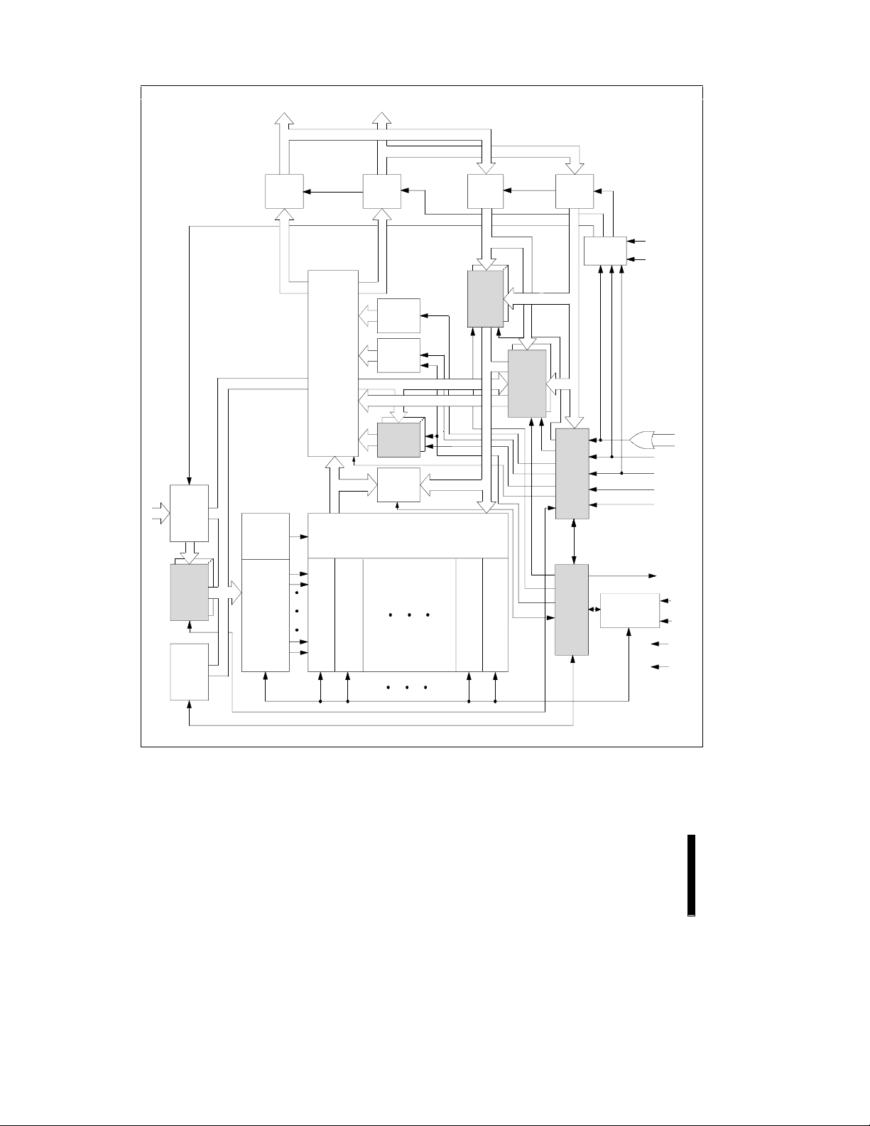
Figure 1. 28F016SV Block Diagram
Architectural Evolution Includes SmartVoltage Technology,
Page Buffers, Queue Registers and Extended Registers
WSM
Program/Erase
Voltage Sw it ch
RY/BY#
V
V
GND
PP
3/5#
CC
0528_01
Page 11
E 28F016SV FlashFile™ MEMORY
2.1 Lead Descriptions
Symbol Type Name and Function
A
0
A1–A
15
A16–A
20
DQ0–DQ7INPUT/OUTPUT LOW-BYTE DATA BUS: Inputs data and commands during CUI program
DQ8–DQ15INPUT/OUTPUT HIGH-BYTE DATA BUS: Inputs data during x16 data program
CE0#, CE1# INPUT CHIP ENABLE INPUTS: Activate the device’s control logic, input buffers,
RP# INPUT RESET/POWER-DOWN: RP# low places the device in a deep power-
OE# INPUT OUTPUT ENABLE: Gates device data through the output buffers when
WE# INPUT WRITE ENABLE: Controls access to the CUI, Page Buffers, Data Queue
INPUT BYTE-SELECT ADDRESS: Selects between high and low byte when
device is in x8 mode. This address is latched in x8 data programs. Not
used in x16 mode (i.e., the A
high).
INPUT WORD-SELECT ADDRESSES: Select a word within one 64-Kbyte block.
A
selects 1 of 1024 rows, and A
6–15
addresses are latched during data programs.
INPUT BLOCK-SELECT ADDRESSES: Select 1 of 32 Erase blocks. These
addresses are latched during data programs, erase and lock block
operations.
cycles. Outputs array, buffer, identifier or status data in the appropriate
read mode. Floated when the chip is de-selected or the outputs are
disabled.
operations. Outputs array, buffer or identifier data in the appropriate read
mode; not used for Status Register reads. Floated when the chip is deselected or the outputs are disabled.
decoders and sense amplifiers. With either CE
is de-selected and power consumption reduces to standby levels upon
completion of any current data program or erase operations. Both CE
# must be low to select the device.
and CE
All timing specifications are the same for both signals. Device Selection
occurs with the latter falling edge of CE
# or CE1# disables the device.
CE
0
down state. All circuits that consume static power, even those circuits
enabled in standby mode, are turned off. When returning from deep
power-down, a recovery time of t
power-up.
When RP# goes low, any current or pending WSM operation(s) are
terminated, and the device is reset. All Status Registers return to ready
(with all status flags cleared).
Exit from deep power-down places the device in read array mode.
low. The outputs float to tri-state off when OE# is high.
CEx# overrides OE#, and OE# overrides WE#.
Registers and Address Queue Latches. WE# is active low, and latches
both address and data (command or array) on its rising edge.
Page Buffer addresses are latched on the falling edge of WE#.
input buffer is turned off when BYTE# is
selects 16 of 512 columns. These
1–5
# or CE
# or CE
is required to allow these circuits to
PHQV
NOTE:
# high, the device
#. The first rising edge of
#
11
Page 12
28F016SV FlashFile™ MEMORY E
2.1 Lead Descriptions (Continued)
Symbol Type Name and Function
RY/BY# OPEN DRAIN
OUTPUT
WP# INPUT WRITE PROTECT: Erase blocks can be locked by writing a nonvolatile
BYTE# INPUT BYTE ENABLE: BYTE# low places device in x8 mode. All data is then
3/5# INPUT 3.3/5.0 VOLT SELECT: 3/5# high configures internal circuits for 3.3V
V
PP
V
CC
SUPPLY PROGRAM/ERASE POWER SUPPLY (12V ± 0.6V, 5V ± 0.5V) : For
SUPPLY DEVICE POWER SUPPLY (3.3V ± 0.3V, 5V ± 0.5V, 5.0 ± 0.25V):
GND SUPPLY GROUND FOR ALL INTERNAL CIRCUITRY:
NC NO CONNECT:
READY/BUSY: Indicates status of the internal WSM. When low, it
indicates that the WSM is busy performing an operation. RY/BY# floating
indicates that the WSM is ready for new operations (or WSM has
completed all pending operations), or erase is suspended, or the device is
in deep power-down mode. This output is always active (i.e., not floated
#, CE
to tri-state off when OE# or CE
# are high), except if a RY/BY# Pin
Disable command is issued.
lock-bit for each block. When WP# is low, those locked blocks as
reflected by the Block-Lock Status bits (BSR.6), are protected from
inadvertent data programs or erases. When WP# is high, all blocks can
be written or erased regardless of the state of the lock-bits. The WP#
input buffer is disabled when RP# transitions low (deep power-down
mode).
input or output on DQ
, and DQ– float. Address A
–
selects between
the high and low byte. BYTE# high places the device in x16 mode, and
turns off the A
input buffer. Address A, then becomes the lowest order
address.
operation. 3/5# low configures internal circuits for 5V operation.
NOTE:
Reading the array with 3/5# high in a 5V system could damage the
device. Reference the power-up and reset timings (Section 5.7) for 3/5#
switching delay to valid data.
erasing memory array blocks or writing words/bytes/pages into the flash
array. V
= 5V ± 0.5V eliminates the need for a 12V converter, while
connection to 12V ± 0.6V maximizes Program/Erase Performance.
NOTE:
Successful completion of program and erase attempts is inhibited with
at or below 1.5V. Program and erase attempts with V
V
between 1.5V
and 4.5V, between 5.5V and 11.4V, and above 12.6V produce spurious
results and should not be attempted.
To switch 3.3V to 5V (or vice versa), first ramp V
then power to the new V
voltage.
CC
down to GND, and
CC
Do not leave any power pins floating.
Do not leave any ground pins floating.
Lead may be driven or left floating.
12
Page 13
E 28F016SV FlashFile™ MEMORY
3/5#
CE #
CE #
A
A
A
A
A
V
A
A
A
A
CE #
V
RP#
A
A
GND
28F016SA28F032SA
3/5#
3/5#
CE #
CE #
1
1
NC
2
20
19
18
17
16
CC
15
14
13
12
0
PP
11
10
A
9
A
8
A
7
A
6
A
5
A
4
A
3
A
2
A
1
A
A
A
A
A
V
A
A
A
A
CE #
V
RP#
A
A
GND
A
20
A
19
A
18
A
17
A
16
V
CC
A
15
A
14
A
13
A
12
CE #
0
V
PP
RP#
A
11
A
10
A
9
A
8
GND
A
7
A
6
A
5
A
4
A
3
A
2
A
1
NC
1
2
1
3
4
20
5
19
6
18
7
17
8
16
9
CC
10
15
11
14
12
13
13
12
14
0
15
PP
16
17
11
18
10
19
A
9
20
A
8
21
22
A
7
23
A
6
24
A
5
25
A
4
26
A
3
27
A
2
28
A
1
E28F016SV
56-LEAD TSOP PINOUT
14 mm x 20 mm
TOP VIEW
NOTE:
56-lead TSOP Mechanical Diagrams and dimensions are shown at the end of this datasheet.
Figure 2. 28F016SV 56-Lead TSOP Pinout Configuration
Shows Compatibility with 28F016SA/28F032SA
56
WP#
55
WE#
54
OE#
53
RY/BY#
52
DQ
51
50
49
48
47
46
45
44
43
42
41
40
39
38
37
36
35
34
33
32
31
30
29
15
DQ
7
DQ
14
DQ
6
GND
DQ
13
DQ
5
DQ
12
DQ
4
V
CC
GND
DQ
11
DQ
3
DQ
10
DQ
2
V
CC
DQ
9
DQ
1
DQ
8
DQ
0
A
0
BYTE#
NC
NC
WP#
WE#
OE#
RY/BY#
DQ
15
DQ
7
DQ
14
DQ
6
GND
DQ
13
DQ
5
DQ
12
DQ
4
V
CC
GND
DQ
11
DQ
3
DQ
10
DQ
2
V
CC
DQ
9
DQ
1
DQ
8
DQ
0
A
0
BYTE#
NC
NC
28F032SA28F016SA
WP#
WE#
OE#
RY/BY#
DQ
15
DQ
7
DQ
14
DQ
6
GND
DQ
13
DQ
5
DQ
12
DQ
4
V
CC
GND
DQ
11
DQ
3
DQ
10
DQ
V
CC
DQ
DQ
DQ
DQ
A
0
BYTE#
NC
NC
0528_02
2
9
1
8
0
13
Page 14
28F016SV FlashFile™ MEMORY E
28F016SA
A
A
A
A
3/5#
NC
A
A
A
A
A
V
DQ
DQ
OE#
DQ
DQ
V
0
1
CC
CC
12
13
14
15
20
19
18
17
16
14
15
13
12
6
7
5
4
CE #
A
A
A
A
3/5#
CE #
NC
A
A
A
A
A
V
GND
DQ
DQ
DQ
DQ
RY/BY#
OE#
WE#
WP#
DQ
DQ
DQ
DQ
V
0
1
CC
1
2
12
3
13
4
14
5
15
6
7
8
9
20
10
19
11
18
17
12
13
16
14
15
6
16
14
17
7
18
15
19
DA28F016SV
56-LEAD SSOP
STANDARD PINOUT
16 mm x 23.7 mm
TOP VIEW
20
21
22
23
24
13
25
5
26
12
27
4
CC
28
CE #
CE #
GND
DQ
DQ
RY/BY#
WE#
WP#
DQ
DQ
NOTE:
56-lead SSOP Mechanical Diagrams and dimensions are shown at the end of this datasheet.
Figure 3. 56-Lead SSOP Pinout Configuration
56
55
54
53
52
51
50
49
48
47
46
45
44
43
42
41
40
39
38
37
36
35
34
33
32
31
30
29
V
PP
R/P#
A
11
A
10
A
9
A
1
A
2
A
3
A
4
A
5
A
6
A
7
GND
A
8
V
CC
DQ
9
DQ
1
DQ
8
DQ
0
A
0
BYTE#
NC
NC
DQ
2
DQ
10
DQ
3
DQ
11
GND
V
PP
R/P#
A
11
A
10
A
9
A
1
A
2
A
3
A
4
A
5
A
6
A
7
GND
A
8
V
CC
DQ
9
DQ
1
DQ
8
DQ
0
A
0
BYTE#
NC
NC
DQ
2
DQ
10
DQ
3
DQ
11
GND
0528_03
28F016SA
14
Page 15
E 28F016SV FlashFile™ MEMORY
e
3.0 MEMORY MAPS
A
[20-0]
1FFFFF
1F0000
1EFFFF
1E0000
1DFFFF
1D0000
1CFFFF
1C0000
1BFFFF
1B0000
1AFFFF
1A0000
19FFFF
190000
18FFFF
180000
17FFFF
170000
16FFFF
160000
15FFFF
150000
14FFFF
140000
13FFFF
130000
12FFFF
120000
11FFFF
110000
10FFFF
100000
0FFFFF
0F0000
0EFFFF
0E0000
0DFFFF
0D0000
0CFFFF
0C0000
0BFFFF
0B0000
0AFFFF
0A0000
09FFFF
090000
08FFFF
080000
07FFFF
070000
06FFFF
060000
05FFFF
050000
04FFFF
040000
03FFFF
030000
02FFFF
020000
01FFFF
010000
00FFFF
000000
64-Kbyte Block
64-Kbyte Block
64-Kbyte Block
64-Kbyte Block
64-Kbyte Block
64-Kbyte Block
64-Kbyte Block
64-Kbyte Block
64-Kbyte Block
64-Kbyte Block
64-Kbyte Block
64-Kbyte Block
64-Kbyte Block
64-Kbyte Block
64-Kbyte Block
64-Kbyte Block
64-Kbyte Block
64-Kbyte Block
64-Kbyte Block
64-Kbyte Block
64-Kbyte Block
64-Kbyte Block
64-Kbyte Block
64-Kbyte Block
64-Kbyte Block
64-Kbyte Block
64-Kbyte Block
64-Kbyte Block
64-Kbyte Block
64-Kbyte Block
64-Kbyte Block
64-Kbyte Block
Byte-Wide (x8) Mode
31
30
29
28
27
26
25
24
23
22
21
20
19
18
17
16
15
14
13
12
11
10
9
8
7
6
5
4
3
2
1
0
A
[20-1]
FFFFF
32-Kword Block
F8000
F7FFF
32-Kword Block
F0000
EFFFF
32-Kword Block
E8000
E7FFF
32-Kword Block
E0000
DFFFF
32-Kword Block
D8000
D7FFF
32-Kword Block
D0000
CFFFF
32-Kword Block
C8000
C7FFF
32-Kword Block
C0000
BFFFF
32-Kword Block
B8000
B7FFF
32-Kword Block
B0000
A8FFF
32-Kword Block
A8000
A7FFF
32-Kword Block
A0000
9FFFF
32-Kword Block
98000
97FFF
32-Kword Block
90000
8FFFF
32-Kword Block
88000
87FFF
32-Kword Block
80000
7FFFF
32-Kword Block
78000
77FFF
32-Kword Block
70000
6FFFF
32-Kword Block
68000
67FFF
32-Kword Block
60000
5FFFF
32-Kword Block
58000
57FFF
32-Kword Block
50000
4FFFF
32-Kword Block
48000
47FFF
32-Kword Block
40000
3FFFF
32-Kword Block
38000
37FFF
32-Kword Block
30000
2FFFF
32-Kword Block
28000
27FFF
32-Kword Block
20000
1FFFF
32-Kword Block
18000
17FFF
32-Kword Block
10000
0FFFF
32-Kword Block
08000
07FFF
32-Kword Block
00000
Word-Wide (x16) Mod
31
30
29
28
27
26
25
24
23
22
21
20
19
18
17
16
15
14
13
12
11
10
9
8
7
6
5
4
3
2
1
0
Figure 4. 28F016SV Memory Maps (Byte-Wide and Word-Wide Modes)
0528_04
15
Page 16
28F016SV FlashFile™ MEMORY E
3.1 Extended Status Registers Memory Map
x8 MODE
RESERVED
GSR
RESERVED
BSR 31
RESERVED
RESERVED
.
.
.
RESERVED
RESERVED
GSR
RESERVED
BSR 0
RESERVED
RESERVED
A[20-0]
1F0006H
1F0005H
1F0004H
1F0003H
1F0002H
1F0001H
1F0000H
010002H
000006H
000005H
000004H
000003H
000002H
000001H
000000H
0528_05
x16 MODE
RESERVED
GSR
RESERVED
BSR 31
RESERVED
RESERVED
.
.
.
RESERVED
RESERVED
GSR
RESERVED
BSR 0
RESERVED
RESERVED
A[20-1]
F8003H
F8002H
F8001H
F8000H
08001H
00003H
00002H
00001H
00000H
0528_06
Figure 5. Extended Status Register Memory
Map (Byte-Wide Mode)
16
Figure 6. Extended Status Register Memory
Map (Word-Wide Mode)
Page 17
E 28F016SV FlashFile™ MEMORY
4.0 BUS OPERATIONS, COMMANDS AND STATUS REGISTER DEFINITIONS
4.1 Bus Operations for Word-Wide Mode (BYTE# = V
Mode Notes RP# CE1#CE0# OE# WE# A
Read 1,2,7 V
Output Disable 1,6,7 V
Standby 1,6,7 V
Deep Power-Down 1,3 V
Manufacturer ID 4 V
Device ID 4,8 V
Write 1,5,6 V
V
IH
V
IH
V
IH
V
V
IL
V
IH
V
IH
V
IH
V
IL
V
IL
V
IL
V
IL
V
V
V
IH
IH
XXXXXHigh Z V
V
IL
V
IL
V
IL
V
IL
V
IL
V
IL
)
IH
DQ
1
V
IL
V
IH
XD
IH
X High Z X
IH
0–15
OUT
RY/BY#
X X X High Z X
V
IL
V
IL
V
IH
V
IH
IH
IL
IL
V
IH
XDINX
0089H V
66A0H V
X
OH
OH
OH
4.2 Bus Operations for Byte-Wide Mode (BYTE# = VIL)
Mode Notes RP# CE1#CE0# OE# WE# A
Read 1,2,7 V
Output Disable 1,6,7 V
Standby 1,6,7 V
Deep Power-Down 1,3 V
Manufacturer ID 4 V
Device ID 4,8 V
Write 1,5,6 V
NOTES:
1. X can be V
2. RY/BY# output is open drain. When the WSM is ready, Erase is suspended or the device is in deep power-down mode.
RY/BY# will be at V
is in progress.
3. RP# at GND ± 0.2V ensures the lowest deep power-down current.
4. A
and A1 at VIL provide device manufacturer codes in x8 and x16 modes respectively. A0 and A1 at VIH provide device ID
0
codes in x8 and x16 modes respectively. All other addresses are set to zero.
5. Commands for erase, data program, or lock-block operations can only be completed successfully when V
V
= V
PP
6. While the WSM is running, RY/BY# in level-mode (default) stays at V
7. RY/BY# may be at V
8. The 28F016SV shares an identical device identifier (66A0H in word-wide mode, A0H in byte-wide mode) with the
PPH2
V
when the WSM is not busy or in erase suspend mode.
OH
program operation).
28F016SA. See application note
differentiate between the 28F016SV and 28F016SA.
for address or control pins except for RY/BY#, which is either V
or V
IH
IL
if it is tied to V
OH
.
while the WSM is busy performing various operations (for example, a Status Register read during a
OL
CC
AP-393 28F016SV Compatibility with 28F016SA
V
IH
V
IH
V
IH
V
V
IL
V
IH
V
IH
V
IH
through a resistor. RY/BY# at V
V
IL
IL
IL
V
IL
V
V
V
IH
IH
XXXXXHigh Z V
V
IL
IL
IL
IL
V
IL
V
IL
OL
V
V
V
IL
IH
IH
V
IH
X X X High Z X
V
V
V
V
IL
IL
IH
OH
until all operations are complete. RY/BY# goes to
IH
V
IH
V
IL
or V
OL
is independent of OE# while a WSM operation
for software and hardware techniques to
DQ
0
XD
0–7
OUT
RY/BY#
X High Z X
V
V
IL
IH
89H V
A0H V
XDINX
.
OH
= V
PP
PPH1
X
OH
OH
OH
or
17
Page 18
28F016SV FlashFile™ MEMORY E
4.3 28F008SA—Compatible Mode Command Bus Definitions
First Bus Cycle Second Bus Cycle
Command Notes Oper Addr Data
(4)
Oper Addr Data
Read Array Write X xxFFH Read AA AD
Intelligent Identifier 1 Write X xx90H Read IA ID
Read Compatible Status Register 2 Write X xx70H Read X CSRD
Clear Status Register 3 Write X xx50H
Word/Byte Program Write X xx40H Write PA PD
Alternate Word/Byte Program Write X xx10H Write PA PD
Block Erase/Confirm Write X xx20H Write BA xxD0H
Erase Suspend/Resume Write X xxB0H Write X xxD0H
ADDRESS DATA
AA = Array Address AD = Array Data
BA = Block Address CSRD = CSR Data
IA = Identifier Address ID = Identifier Data
PA = Program Address PD = Program Data
X = Don’t Care
NOTES:
1. Following the Intelligent Identifier command, two Read operations access the manufacturer and device signature codes.
2. The CSR is automatically available after device enters data program, erase, or suspend operations.
3. Clears CSR.3, CSR.4 and CSR.5. Also clears GSR.5 and all BSR.5, BSR.4 and BSR.2 bits. See Status Register
definitions.
4. The upper byte of the data bus (DQ
) during command writes is a “Don’t Care” in x16 operation of the device.
8–15
(4)
18
Page 19
E 28F016SV FlashFile™ MEMORY
4.4 28F016SV—Performance Enhancement Command Bus Definitions
Command Mode Notes First Bus Cycle Second Bus Cycle Third Bus Cycle
Oper Addr Data
Read Extended
Status Register
Page Buffer Swap 7 Write X xx72H
Read Page Buffer Write X xx75H Read PBA PD
Single Load to Page
Buffer
Sequential Load to
Page Buffer
Page Buffer Write to
Flash
Two-Byte Program x8 3 Write X xxFBH Write A0WD(L,H) Write PA WD(H,L)
Lock Block/Confirm Write X xx77H Write BA xxD0H
Upload Status
Bits/Confirm
Upload Device
Information/Confirm
Erase All Unlocked
Blocks/Confirm
RY/BY# Enable to
Level-Mode
RY/BY#
Pulse-On-Write
RY/BY#
Pulse-On-Erase
RY/BY# Disable 8 Write X xx96H Write X xx04H
RY/BY# Pulse-On-
Write/Erase
Sleep 12 Write X xxF0H
Abort Write X xx80H
ADDRESS DATA
BA = Block Address AD = Array Data WC (L,H) = Word Count (Low, High)
PBA = Page Buffer Address PD = Page Buffer Data BC (L,H) = Byte Count (Low, High)
RA = Extended Register Address BSRD = BSR Data WD (L,H) = Write Data (Low, High)
PA = Program Address GSRD = GSR Data
X = Don’t Care
x8 4,6,10 Write X xxE0H Write X BCL Write X BCH
x16 4,5,6,10 Write X xxE0H Write X WCL Write X WCH
x8 3,4,9,10 Write X xx0CH Write A0BC(L,H) Write PA BC(H,L)
x16 4,5,10 Write X xx0CH Write X WCL Write PA WCH
1 Write X xx71H Read RA GSRD
Write X xx74H Write PBA PD
2 Write X xx97H Write X xxD0H
11 Write X xx99H Write X xxD0H
Write X xxA7H Write X xxD0H
8 Write X xx96H Write X xx01H
8 Write X xx96H Write X xx02H
8 Write X xx96H Write X xx03H
8 Write X xx96H Write X xx05H
(13)
Oper Addr Data
BSRD
(13)
Oper Addr Data
19
Page 20

28F016SV FlashFile™ MEMORY E
NOTES:
1. RA can be the GSR address or any BSR address. See Figures 4 and 5 for Extended Status Register memory maps.
2. Upon device power-up, all BSR lock-bits come up locked. The Upload Status Bits command must be written to reflect the
actual lock-bit status.
3. A
is automatically complemented to load second byte of data. BYTE# must be at VIL.
0
A
value determines which WD/BC is supplied first: A0 = 0 looks at the WDL/BCL, A0 = 1 looks at the WDH/BCH.
0
4. BCH/WCH must be at 00H for this product because of the 256-byte (128-word) Page Buffer size, and to avoid writing the
Page Buffer contents to more than one 256-byte segment within an array block. They are simply shown for future Page
Buffer expandability.
5. In x16 mode, only the lower byte DQ
6. PBA and PD (whose count is given in cycles 2 and 3) are supplied starting in the fourth cycle, which is not shown.
7. This command allows the user to swap between available Page Buffers (0 or 1).
8. These commands reconfigure RY/BY# output to one of three pulse-modes or enable and disable the RY/BY# function.
9. Program address, PA, is the Destination address in the flash array which must match the Source address in the Page
Buffer. Refer to the
16-Mbit Flash Product Family User’s Manual
10. BCL = 00H corresponds to a byte count of 1. Similarly, WCL = 00H corresponds to a word count of 1.
11. After writing the Upload Device Information command and the Confirm command, the following information is output at
Page Buffer addresses specified below:
Address Information
06H, 07H (Byte Mode) Device Revision Number
03H (Word Mode) Device Revision Number
1EH (Byte Mode) Device Configuration Code
0FH (DQ
1FH (Byte Mode) Device Proliferation Code (01H)
0FH (DQ
)(Word Mode) Device Configuration Code
–
)(Word Mode) Device Proliferation Code (01H)
–
A page buffer swap followed by a page buffer read sequence is necessary to access this information. The contents of all
other Page Buffer locations, after the Upload Device Information command is written, are reserved for future implementation
by Intel Corporation. See Section 4.8 for a description of the Device Configuration Code. This code also corresponds to
data written to the 28F016SV after writing the RY/BY# Reconfiguration command.
12. To ensure that the 28F016SV’s power consumption during sleep mode reaches the deep power-down current level, the
system also needs to de-select the chip by taking either or both CE
13. The upper byte of the data bus (DQ
is used for WCL and WCH. The upper byte DQ
0–7
is a don’t care.
8–15
.
# or CE1# high.
) during command writes is a “Don’t Care” in x16 operation of the device.
8–15
0
20
Page 21

E 28F016SV FlashFile™ MEMORY
4.5 Compatible Status Register
WSMS ESS ES DWS VPPS R R R
76543210
NOTES:
CSR.7 = WRITE STATE MACHINE STATUS
1 = Ready
0 = Busy
CSR.6 = ERASE-SUSPEND STATUS
1 = Erase Suspended
0 = Erase in Progress/Completed
RY/BY# output or WSMS bit must be checked to
determine completion of an operation (erase,
erase suspend, or data program) before the
appropriate Status bit (ESS, ES or DWS) is
checked for success.
CSR.5 = ERASE STATUS
1 = Error in Block Erasure
0 = Successful Block Erase
CSR.4 = DATA-WRITE STATUS
1 = Error in Data Program
0 = Data Program Successful
CSR.3 = V
CSR.2–0 = RESERVED FOR FUTURE ENHANCEMENTS
These bits are reserved for future use; mask them out when polling the CSR.
STATUS
Error Detect, Operation Abort
1 = V
OK
0 = V
If DWS and ES are set to “1” during an erase
attempt, an improper command sequence was
entered. Clear the CSR and attempt the
operation again.
The VPPS bit, unlike an A/D converter, does not
provide continuous indication of V
WSM interrogates V
Program or Erase command sequences have
been entered, and informs the system if V
not been switched on. VPPS is not guaranteed to
report accurate feedback between V
and V
V
(min), between V
(min) and above V
level. The
’s level only after the Data
has
(max)
(max) and
(max).
21
Page 22

28F016SV FlashFile™ MEMORY E
4.6 Global Status Register
WSMS OSS DOS DSS QS PBAS PBS PBSS
76543210
NOTES:
GSR.7 = WRITE STATE MACHINE STATUS
1 = Ready
0 = Busy
GSR.6 = OPERATION SUSPEND STATUS
1 = Operation Suspended
0 = Operation in Progress/Completed
GSR.5 = DEVICE OPERATION STATUS
1 = Operation Unsuccessful
0 = Operation Successful or Currently
Running
GSR.4 = DEVICE SLEEP STATUS
1 = Device in Sleep
0 = Device Not in Sleep
MATRIX 5/4
0 0 = Operation Successful or Currently
Running
0 1 = Device in Sleep Mode or Pending
Sleep
1 0 = Operation Unsuccessful
1 1 = Operation Unsuccessful or
Aborted
[1]
RY/BY# output or WSMS bit must be checked
to determine completion of an operation (block
lock, suspend, any RY/BY# reconfiguration,
Upload Status Bits, erase or data program)
before the appropriate Status bit (OSS or DOS)
is checked for success.
If operation currently running, then GSR.7 = 0.
If device pending sleep, then GSR.7 = 0.
Operation aborted: Unsuccessful due to Abort
command.
GSR.3 = QUEUE STATUS
1 = Queue Full
0 = Queue Available
GSR.2 = PAGE BUFFER AVAILABLE STATUS
The device contains two Page Buffers.
1 = One or Two Page Buffers Available
0 = No Page Buffer Available
GSR.1 = PAGE BUFFER STATUS
1 = Selected Page Buffer Ready
Selected Page Buffer is currently busy with WSM
operation
0 = Selected Page Buffer Busy
GSR.0 = PAGE BUFFER SELECT STATUS
1 = Page Buffer 1 Selected
0 = Page Buffer 0 Selected
NOTE:
1. When multiple operations are queued, checking BSR.7 only provides indication of completion for that particular block.
GSR.7 provides indication when all queued operations are completed.
22
Page 23

E 28F016SV FlashFile™ MEMORY
(max) and V
(max) and V
4.7 Block Status Register
BS BLS BOS BOAS QS VPPS VPPL R
76543210
NOTES:
BSR.7 = BLOCK STATUS
BSR.6 = BLOCK LOCK STATUS
BSR.5 = BLOCK OPERATION STATUS
BSR.4 = BLOCK OPERATION ABORT STATUS
MATRIX 5/4
BSR.3 = QUEUE STATUS
BSR.2 = V
BSR.1 = V
BSR.0 = RESERVED FOR FUTURE ENHANCEMENTS
This bits is reserved for future use; mask it out when polling the BSRs.
NOTE:
1. When multiple operations are queued, checking BSR.7 only provides indication of completion or that particular block.
GSR.7 provides indication when all queued operations are completed.
1 = Ready
0 = Busy
1 = Block Unlocked for Program/Erase
0 = Block Locked for Program/Erase
1 = Operation Unsuccessful
0 = Operation Successful or
Currently Running
1 = Operation Aborted
0 = Operation Not Aborted
0 0 = Operation Successful or
Currently Running
0 1 = Not a Valid Combination
1 0 = Operation Unsuccessful
1 1 = Operation Aborted Operation halted via Abort command.
1 = Queue Full
0 = Queue Available
STATUS
1 = V
Error Detect, Operation Abort
0 = V
OK
LEVEL
1 = V
Detected at 5V ± 10%
0 = V
Detected at 12V ± 5%
[1]
RY/BY# output or BS bit must be checked to
determine completion of an operation (block lock,
suspend, erase or data program) before the
appropriate Status bits (BOS, BLS) is checked
for success.
The BOAS bit will not be set until BSR.7 = 1.
BSR.1 is not guaranteed to report accurate
feedback between the V
ranges. Programs and erases with V
V
V
V
(max) produce spurious results and should
not be attempted.
BSR.1 was a RESERVED bit on the 28F016SA.
and V
(min), between
(min), and above
voltage
between
23
Page 24

28F016SV FlashFile™ MEMORY E
4.8 Device Configuration Code
R R R R R RB2 RB1 RB0
76543210
NOTES:
DCC.2-DCC.0 = RY/BY# CONFIGURATION
(RB2–RB0)
001 =Level Mode (Default)
010 =Pulse-On-Program
011 = Pulse-On-Erase
100 = RY/BY# Disabled
101 = Pulse-On-Program/Erase
DCC.7–DCC.3 = RESERVED FOR FUTURE ENHANCEMENTS
These bits are reserved for future use; mask them out when reading the Device Configuration Code.
Set these bits to “0” when writing the desired RY/BY# configuration to the device.
Undocumented combinations of RB2–RB0 are
reserved by Intel Corporation for future
implementations and should not be used.
24
Page 25

E 28F016SV FlashFile™ MEMORY
5.0 ELECTRICAL SPECIFICATIONS
5.1 Absolute Maximum Ratings*
Temperature Under Bias ....................0°C to +80°C
Storage Temperature ...................–65°C to +125°C
VCC = 3.3V ± 0.3V Systems
Sym Parameter Notes Min Max Units Test Conditions
T
Operating Temperature, Commercial 1 0 70 °C Ambient Temperature
A
V
CCVCC
V
PPVPP
V
I Current into Any Non-Supply Pin 5 ± 30 mA
I
OUT
V
CC
Sym Parameter Notes Min Max Units Test Conditions
T
A
V
CCVCC
V
PPVPP
V
I Current into Any Non-Supply Pin 5 ± 30 mA
with Respect to GND 2 –0.2 7.0 V
Supply Voltage with Respect to GND 2,3 –0.2 14.0 V
Voltage on Any Pin (except V
Respect to GND
Output Short Circuit Current 4 100 mA
= 5V ± 0.5V, 5V ± 0.25V Systems
Operating Temperature, Commercial 1 0 70 °C Ambient Temperature
with Respect to GND 2 –0.2 7.0 V
Supply Voltage with Respect to GND 2,3 –0.2 14.0 V
Voltage on Any Pin (except V
Respect to GND
CC,VPP
(6)
CC,VPP
) with
) with
NOTICE: This is a production datasheet. The
specifications are subject to change without notice. Verify
with your local Intel Sales office that you have the latest
datasheet before finalizing a design.
*WARNING: Stressing the device beyond the “Absolute
Maximum Ratings” may cause permanent damage.
These are stress ratings only. Operation beyond the
“Operating Conditions” is not recommended and
extended exposure beyond the "Operating Conditions"
may affect device reliability.
V
2,5 –0.5
2,5 –2.0 7.0 V
CC
+ 0.5
V
I
Output Short Circuit Current 4 100 mA
OUT
NOTES:
1. Operating temperature is for commercial product defined by this specification.
2. Minimum DC voltage is –0.5V on input/output pins. During transitions, this level may undershoot to –2.0V for periods
<20 ns. Maximum DC voltage on input/output pins is V
periods <20 ns.
3. Maximum DC voltage on V
4. Output shorted for no more than one second. No more than one output shorted at a time.
5. This specification also applies to pins marked “NC.”
6. 5% V
specifications refer to the 28F016SV-065 and 28F016SV-070 in its high speed test configuration.
CC
may overshoot to +14.0V for periods <20 ns.
PP
+ 0.5V which, during transitions, may overshoot to VCC + 2.0V for
CC
25
Page 26

28F016SV FlashFile™ MEMORY E
5.2 Capacitance
For a 3.3V ± 0.3V System:
Sym Parameter Notes Typ Max Units Test Conditions
C
IN
C
OUT
C
LOAD
For 5V ± 0.5V, 5V ± 0.25V System:
C
IN
C
OUT
C
LOAD
NOTE:
1. Sampled, not 100% tested. Guaranteed by design.
2. To obtain iBIS models for the 28F016SV, please contact your local Intel/Distribution Sales Office.
Capacitance Looking into an
168pFT
= +25°C, f = 1.0 MHz
A
Address/Control Pin
Capacitance Looking into an
1 8 12 pF T
= +25°C, f = 1.0 MHz
A
Output Pin
Load Capacitance Driven by
1,2 50 pF
Outputs for Timing Specifications
Sym Parameter Notes Typ Max Units Test Conditions
Capacitance Looking into an
168pFT
= +25°C, f = 1.0 MHz
A
Address/Control Pin
Capacitance Looking into an
1 8 12 pF TA = +25°C, f = 1.0 MHz
Output Pin
Load Capacitance Driven by
1,2 100 pF For VCC = 5V ± 0.5V
Outputs for Timing Specifications
30 pF For VCC = 5V ± 0.25V
26
Page 27

E 28F016SV FlashFile™ MEMORY
2.4
INPUT OUTPUT
0.45
AC test inputs are driven at VOH (2.4 VTTL) for a Logic “1” and VOL (0.45 VTTL) for a Logic “0.” Input timing begins at V
(2.0 VTTL) and VIL (0.8 VTTL). Output timing ends at VIH and VIL. Input rise and fall times (10% to 90%) <10 ns.
Figure 7. Transient Input/Output Reference Waveform for
V
CC
3.0
0.0
AC test inputs are driven at 3.0V for a Logic “1” and 0.0V for a Logic “0.” Input timing begins, and output timing ends, at 1.5V.
Input rise and fall times (10% to 90%) <10 ns.
Figure 8. Transient Input/Output Reference Waveform for VCC = 3.3V ± 0.3V
NOTES:
1. Testing characteristics for 28F016SV-070 (Standard Testing Configuration) and 28F016SV-080.
2. Testing characteristics for 28F016SV-065/28F016SV-075 and 28F016SV-70 (High Speed Testing Configuration)/
28F016SV-120.
and V
2.0
TEST POINTS
0.8 0.8
= 5V ± 10% (Standard Testing Configuration)
1.5
= 5V ± 5% (High Speed Testing Configuration)
CC
TEST POINTSINPUT
(1)
1.5
2.0
IH
0528_07
OUTPUT
0528_08
(2)
27
Page 28

28F016SV FlashFile™ MEMORY E
2.5 ns of 25 Transmission Line
From Output
under Test
Ω
Total Capacitance = 100 pF
Figure 9. Transient Equivalent Testing Load Circuit
From Output
under Test
(28F016SV-070/-080 at V
2.5 ns of 50 Transmission Line
Ω
= 5V ± 10%)
CC
Total Capacitance = 50 pF
Figure 10. Transient Equivalent Testing Load Circuit
(28F016SV-075/-120 at V
= 3.3V ± 0.3V)
CC
Test
Point
0528_09
Test
Point
0528_10
28
2.5 ns of 83
From Output
under Test
Ω
Transmission Line
Test
Point
Total Capacitanc e = 30 pF
Figure 11. High Speed Transient Equivalent Testing Load Circuit
(28F016SV-065/-070 at V
= 5V ± 5%)
CC
0528_11
Page 29

E 28F016SV FlashFile™ MEMORY
5.3 DC Characteristics
VCC = 3.3V ± 10%V, TA = 0°C to +70°C, –40°C to +70°C
3/5# = Pin Set High for 3.3V Operations
Temp Commercial Extended
Sym Parameter Notes Min Typ Max Min Typ Max Units Test Conditions
I
Input Load
LI
Current
I
Output
LO
Leakage
Current
I
CCSVCC
Current
I
CCDVCC
Power-Down
Current
I
1VCC Read
CCR
Current
Standby
Deep
1 ± 1 ± 1µAVCC = VCC Max
V
= VCC or GND
IN
1 ± 10 ± 10 µA V
1,5 70 130 70 130 µA VCC = V
1 4 1 4 mA VCC = VCC Max
1 2 10 5 15 µA RP# = GND ± 0.2V
1,4,5 40 50 40 55 mA VCC = VCC Max
= VCC Max
CC
V
= VCC or GND
OUT
Max
CC
#, CE
CE
BYTE#, WP#, 3/5#
CE
BYTE#, WP#, 3/5#
BYTE# = V
CMOS: CE
TTL: CE
or V
f = 8 MHz, I
#, RP# =
V
± 0.2V
CC
±0.2V or
= V
CC
GND ± 0.2V
#, CE1#, RP# =
0
V
IH
or V
= V
IH
CC
0.2V or GND ±
0.2V
#, CE1#
0
= GND ± 0.2V,
BYTE# = GND ±
0.2V or V
0.2V, Inputs =
GND ± 0.2V or
V
V
V
0 mA
CC
± 0.2V
CC
#, CE1# =
0
, BYTE# = V
IL
Inputs =
or V
IL
IH
OUT
IL
±
±
IL
=
29
Page 30

28F016SV FlashFile™ MEMORY E
5.3 DC Characteristics (Continued)
= 3.3V ± 10%V, TA = 0°C to +70°C, –40°C to +70°C
V
CC
3/5# = Pin Set High for 3.3V Operations
Temp Commercial Extended
Sym Parameter Notes Min Typ Max Min Typ Max Units Test Conditions
I
2VCC Read
CCR
Current
I
CCWVCC
Program
Current for
Word or Byte
I
CCEVCC
Block
Erase
Current
I
CCESVCC
Erase
Suspend
Current
I
PPSVPP
I
PPR
I
PPDVPP
Standby/ 1 ± 1 ± 10 ± 3 ± 10 µA VPP ≤ V
Read Current 30 200 70 200 µA VPP > V
Deep
Power-Down
Current
1,4,
5,6
20 30 20 35 mA VCC = VCC Max
CMOS: CE
#, CE1#
0
= GND ± 0.2V,
BYTE# = GND ±
0.2V or V
CC
0.2V, Inputs =
GND ± 0.2V or
± 0.2V
V
CC
TTL: CE
f = 4 MHz, I
#, CE1# =
0
V
, BYTE# = V
IL
or V
Inputs =
IH,
V
or V
IL
IH
OUT
0 mA
1,6 8 12 8 12 mA V
= 12V ± 5%
PP
Program in
Progress
8 17 8 17 mA VPP = 5V ± 10%
Program in
Progress
1,6 6 12 6 12 mA VPP = 12V ± 5%
Block Erase in
Progress
9 17 9 17 mA VPP = 5V ± 10%
Block Erase in
Progress
1,2 1 4 1 4 mA CE0#, CE1# = V
Block Erase
Suspended
CC
CC
1 0.2 5 0.2 5 µA RP# = GND ± 0.2V
±
IL
=
IH
30
Page 31

E 28F016SV FlashFile™ MEMORY
5.3 DC Characteristics (Continued)
= 3.3V ± 10%V, TA = 0°C to +70°C, –40°C to +70°C
V
CC
3/5# = Pin Set High for 3.3V Operations
Temp Commercial Extended
Sym Parameter Notes Min Typ Max Min Typ Max Units Test Conditions
I
PPWVPP
I
PPEVPP
I
PPESVPP
V
IL
V
IH
V
OL
Program
Current for
Word or Byte
Erase
Current
Erase
Suspend
Current
Input Low
Voltage
Input High
Voltage
Output Low
Voltage
1,6 10 15 10 15 mA VPP = 12V ± 5%
Program in
Progress
15 25 15 25 mA VPP = 5V ± 10%
Program in
Progress
1,6 4 10 4 10 mA VPP = 12V ± 5%
Block Erase in
Progress
14 20 14 20 mA VPP = 5V ± 10%
Block Erase in
Progress
1 30 200 70 200 µA V
6 –0.3 0.8 0.8 V
6 2.0 V
6 0.4 0.4 V VCC = VCC Min and
CC
+ 0.3
V
+ 0.3
V
= V
V
PPH2
Block Erase
Suspended
I
= 4 mA
OL
or
31
Page 32

28F016SV FlashFile™ MEMORY E
K
5.3 DC Characteristics (Continued)
V
= 3.3V ± 0.3V, TA = 0°C to +70°C, –40°C to +85°C
CC
3/5# = Pin Set High for 3.3V Operations
Temp Comm/Ext
Sym Parameter Notes Min Typ Max Units Test Conditions
= 3.3V, V
(min) and above V
PPH2
VV
PP
= VCC Min
CC
= –2.0 mA
I
OH
I
= –100 µA
OH
= 12V or 5V, T = +25°C. These currents
≤ V
PP
and not guaranteed in the
PPLK
PPH2
(max).
VOH1 Output High
Voltage
6 2.4
V
CC
–
VOH2 6 0.2 V VCC = VCC Min
V
PPL
VPP Program/Erase
3,6 0.0 1.5 V
Lock Voltage
V
PPH1
VPP during
3 4.5 5.0 5.5 V
Program/Erase
Operations
V
PPH2
VPP during
3 11.4 12.0 12.6 V
Program/Erase
Operations
V
LKO
VCC Program/Erase
2.0 V
Lock Voltage
NOTES:
1. All currents are in RMS unless otherwise noted. Typical values at V
are valid for all product versions (package and speeds).
2. I
is specified with the device de-selected. If the device is read while in erase suspend mode, current draw is the sum of
CCES
I
and I
CCES
3. Block erases, word/byte programs and lock block operations are inhibited when V
ranges between V
4. Automatic Power Savings (APS) reduces I
5. CMOS Inputs are either V
6. Sampled, but not 100% tested. Guaranteed by design.
CCR
.
(max) and V
PPLK
(min), between V
PPH1
± 0.2V or GND ± 0.2V. TTL Inputs are either VIL or VIH.
CC
CCR
PPH1
to 3.0 mA typical in static operation.
CC
(max) and V
32
Page 33

E 28F016SV FlashFile™ MEMORY
5.4 DC Characteristics
VCC = 5V ± 0.5V, 5V ± 0.25V, TA = 0°C to +70°C, –40°C to +85°C
3/5# = Pin Set Low for 5V Operations
Temp Commercial Extended
Sym Parameter Notes Min Typ Max Min Typ Max Units Test Conditions
I
LI
I
LO
I
CCS
I
CCD
I
1VCC Read
CCR
Input Load
Current
Output
Leakage
Current
VCC Standby
Current
VCC Deep
Power-Down
Current
Current
1± 1± 1µAV
1 ± 10 ± 10 µA V
1,5 70 130 70 130 µA V
= V
CC
CC
V
= V
IN
CC
= V
CC
CC
V
= V
OUT
= V
CC
CC
#, CE1#, RP# =
CE
0
V
± 0.2V
CC
Max
or GND
Max
or GND
CC
Max
BYTE#, WP#, 3/5#
± 0.2V or
= V
CC
GND ± 0.2V
2 4 2 4 mA VCC = VCC Max,
CE
#, CE1#, RP# =
0
V
IH
BYTE#, WP#, 3/5#
or V
= V
IH
IL
1 2 10 5 15 µA RP# = GND ± 0.2V
BYTE# = V
CC
±
0.2V or GND ±
0.2V
1,4,5 75 95 75 105 mA VCC = VCC Max
CMOS: CE
#, CE1#
0
= GND ± 0.2V,
BYTE# = GND ±
0.2V or V
CC
±
0.2V, Inputs =
GND ± 0.2V or,
± 0.2V
V
CC
TTL: CE
V
or V
V
f = 10 MHz, I
#, CE1# =
0
, BYTE# = V
IL
Inputs =
IH,
or V
IL
IH
OUT
=
0 mA
IL
33
Page 34

28F016SV FlashFile™ MEMORY E
5.4 DC Characteristics (Continued)
= 5V ± 0.5V, 5V ± 0.25V, TA = 0°C to +70°C, –40°C to +85°C
V
CC
3/5# = Pin Set Low for 5V Operations
Temp Commercial Extended
Sym Parameter Notes Min Typ Max Min Typ Max Units Test Conditions
I
2VCC Read
CCR
Current
I
CCWVCC
Program
Current for
Word or Byte
I
CCEVCC
Block
Erase
Current
I
CCESVCC
Erase
Suspend
Current
I
VPP Standby
PPS
/Read
I
Current 30 200 70 200 µA V
PPR
I
V
PPD
Deep
PowerDown Current
1,4,
5,6
45 55 45 60 mA VCC = VCC Max
CMOS: CE
#, CE1#
0
= GND ± 0.2V,
BYTE# = GND ±
0.2V or V
CC
0.2V, Inputs =
GND ± 0.2V or
± 0.2V
V
CC
TTL: CE
V
#, CE1# =
0
, BYTE# = V
IL
or VIH, Inputs =
V
or V
IL
f = 5 MHz, I
IH
OUT
0 mA
1,6 25 35 25 35 mA VPP = 12V ± 5%
Program in
Progress
25 40 25 40 mA VPP = 5V ± 10%
Program in
Progress
1,6 18 25 18 25 mA VPP = 12V ± 5%
Block Erase in
Progress
20 30 20 30 mA VPP = 5V ± 10%
Block Erase in
Progress
1,2 2 4 2 4 mA CE
#, CE1# = V
0
Block Erase
Suspended
1 ± 1 ± 10 ± 3 ± 10 µA V
PP
PP
≤ V
> V
CC
CC
1 0.2 5 0.2 5 µA RP# = GND ± 0.2V
±
=
IH
IL
34
Page 35

E 28F016SV FlashFile™ MEMORY
5.4 DC Characteristics (Continued)
= 5V ± 0.5V, 5V ± 0.25V, TA = 0°C to +70°C, –40°C to +85°C
V
CC
3/5# = Pin Set Low for 5V Operations
Temp Commercial Extended
Sym Parameter Notes Min Typ Max Min Typ Max Units Test Conditions
I
V
PPW
I
PPEVPP
I
PPES
V
IL
V
IH
Program
Current for
Word or Byte
Block
Erase
Current
VPP Erase
Suspend
Current
Input Low
Voltage
Input High
Voltage
1,6 7 12 7 12 mA V
17 22 17 22 mA V
1,6 5 10 5 10 mA V
16 20 16 20 mA V
1 30 200 30 200 µA V
6 –0.5 0.8 0.8 V
6 2.0 VCC+
0.5
VCC+
0.5
V
PP
Program in
PP
Program in
PP
Block Erase in
PP
Block Erase in
Block Erase
± 5%
= 12V
Progress
± 10%
= 5V
Progress
± 5%
= 12V
Progress
± 10%
= 5V
Progress
= V
V
Suspended
or
PPH2
35
Page 36

28F016SV FlashFile™ MEMORY E
K
5.4 DC Characteristics (Continued)
= 5V ± 0.5V, 5V ± 0.25V, TA = 0°C to +70°C, –40°C to +85°C
V
CC
3/5# = Pin Set Low for 5V Operations
Temp Comm/Extended
Sym Parameter Notes Min Typ Max Units Test Conditions
V
OL
VOH1 Output High
VOH26V
V
PPL
Output Low Voltage 6 0.45 V V
Voltage
6 0.85
V
CC
CC
–
VVCC = VCC Min
0.4
VPP Program/Erase
3,6 0.0 1.5 V
CC
I
= 5.8 mA
OL
I
= –2.5 mA
OH
V
CC
I
= –100 µA
OH
= V
= V
CC
CC
Min
Min
Lock Voltage
V
PPH1
VPP during
4.5 5.0 5.5 V
Program/Erase
Operations
V
PPH2
VPP during
11.4 12.0 12.6 V
Program/Erase
Operations
V
LKO
VCC Program/Erase
2.0 V
Lock Voltage
NOTES:
1. All currents are in RMS unless otherwise noted. Typical values at V
valid for all product versions (package and speeds) and are specified for a CMOS rise/fall time (10% to 90%) of <5 ns and a
TTL rise/fall time of <10 ns.
2. I
is specified with the device de-selected. If the device is read while in erase suspend mode, current draw is the sum of
CCES
I
and I
CCES
3. Block erases, word/byte programs and lock block operations are inhibited when VPP ≤ V
ranges between V
4. Automatic Power Saving (APS) reduces I
5. CMOS Inputs are either V
6. Sampled, not 100% tested. Guaranteed by design.
CCR.
(max) and V
PPLK
(min), between V
PPH1
± 0.2V or GND ± 0.2V. TTL Inputs are either VIL or VIH.
CC
to 1 mA typical in Static operation.
CCR
PPH1
= 5V, VPP =
CC
(max) and V
12V
(min) and above V
PPH2
or 5V, T = 25°C. These currents are
and not guaranteed in the
PPLK
PPH2
(max).
36
Page 37

E 28F016SV FlashFile™ MEMORY
5.5 Timing Nomenclature
All 3.3V system timings are measured from where signals cross 1.5V.
For 5V systems use the standard JEDEC cross point definitions (standard testing) or from where signals
cross 1.5V (high speed testing).
Each timing parameter consists of 5 characters. Some common examples are defined below:
t
CEtELQV
t
OEtGLQV
t
ACCtAVQV
t
AS
t
DHtWHDX
5V VCC at 4.5V Minimum
3V VCC at 3.0V Minimum
time(t) from CE# (E) going low (L) to the outputs (Q) becoming valid (V)
time(t) from OE # (G) going low (L) to the outputs (Q) becoming valid (V)
time(t) from address (A) valid (V) to the outputs (Q) becoming valid (V)
t
time(t) from address (A) valid (V) to WE# (W) going high (H)
AVWH
time(t) from WE# (W) going high (H) to when the data (D) can become undefined (X)
Pin Characters Pin States
A Address Inputs H High
D Data Inputs L Low
Q Data Outputs V Valid
E CE# (Chip Enable) X Driven, but Not Necessarily Valid
F BYTE# (Byte Enable) Z High Impedance
G OE# (Output Enable)
W WE# (Write Enable)
P RP# (Deep Power-Down Pin)
R RY/BY# (Ready Busy)
V Any Voltage Level
Y 3/5# Pin
37
Page 38

28F016SV FlashFile™ MEMORY E
5.6 AC Characteristics—Read Only Operations
V
= 3.3V ± 0.3V, TA = 0°C to +70°C, –40°C to +85°C
CC
(1)
Temp Commercial Extended Commercial
Sym Parameter Speed –75 –100 –120 Units
Notes Min Max Min Max Min Max
t
Read Cycle Time 75
AVAV
t
Address to Output Delay 75
AVQV
t
CE# to Output Delay 2,8 75
ELQV
t
RP# High to Output
PHQV
85
(10)
85
85
(10)
(10)
480
100
120 ns
100
100
620
120 ns
120 ns
620 ns
Delay
t
OE# to Output Delay 2 40
GLQV
t
CE# to Output in Low Z 3,8 0
ELQX
t
CE# to Output in High Z 3,8 30
EHQZ
t
OE# to Output in Low Z 3 0
GLQX
t
OE# to Output in High Z 3 20
GHQZ
t
Output Hold from
OH
3,8 0
45
0
50
0
20
0
45 ns
0ns
50 ns
0ns
20 ns
0ns
Address, CE# or OE#
Change, Whichever
Occurs First
t
BYTE# to Output Delay 3 75
FLQV
t
FHQV
t
BYTE# Low to Output in
FLQZ
330 3030ns
85
(10)
100 120 ns
High Z
t
CE# Low to BYTE# High
ELFL
or Low
t
ELFH
3,8 5 5 5 ns
Extended Status Register Reads
t
Address Setup to CE#
AVEL
Going Low
t
Address Setup to OE#
AVGL
Going Low
38
3,4,
8,9
3,4,9 0 0 0 ns
000ns
Page 39

E 28F016SV FlashFile™ MEMORY
5.6 AC Characteristics—Read Only Operations
V
= 5V ± 0.5V, 5V ± 0.25V, TA = 0°C to +70°C, –40°C to +85°C
CC
Temp Commercial Comm/Ext
Speed –65 –70 –80
Sym Parameter V
t
t
t
t
t
t
t
t
t
t
t
t
t
t
t
Read Cycle Time 65 70 80 ns
AVAV
Address to Output Delay 65 70 80 ns
AVQV
CE# to Output Delay 2,8 65 70 80 ns
ELQV
RP# to Output Delay 400 480
PHQV
OE# to Output Delay 2 30 30
GLQV
CE# to Output in Low Z 3,8 0 0 0 ns
ELQX
CE# to Output in High Z 3,8 25 25 30 ns
EHQZ
OE# to Output in Low Z 3 0 0 0 ns
GLQX
OE# to Output in High Z 3 15 15 20 ns
GHQZ
Output Hold from
OH
Address, CE# or OE#
Change, Whichever
Occurs First
BYTE# to Output Delay 3 65 70 80 ns
FLQV
FHQV
BYTE# Low to Output in
FLQZ
High Z
CE# Low to BYTE#
ELFL
High or Low
ELFH
CC 5V
Load 30 pF 50 pF 50 pF
Notes Min Max Min Max Min Max
3,8 0 0 0 ns
3 252530ns
3,8 5 5 5 ns
± 5%V
(1)
(Continued)
5V
± 10%
400
35
± 10% Units
5V
(6)
(7)
(6)
(7)
480 ns
35 ns
Extended Status Register Reads
t
t
Address Setup to CE#
AVEL
Going Low
Address Setup to OE#
AVGL
Going Low
3,4,8,9 0 0 0 ns
3,4,9 0 0 0 ns
39
Page 40

28F016SV FlashFile™ MEMORY E
NOTES:
1. See AC Input/Output Reference Waveforms for timing measurements, Figures 7 and 8.
2. OE# may be delayed up to t
ELQV-tGLQV
3. Sampled, not 100% tested. Guaranteed by design
4. This timing parameter is used to latch the correct BSR data onto the outputs.
5. Device speeds are defined as:
65/70 ns at V
75 ns at V
70/80 ns at V
120 ns at V
= 5V equivalent to
CC
= 3.3V
CC
= 5V equivalent to
CC
= 3.3V
CC
6. See the high speed AC Input/Output Reference Waveforms and AC Testing Load Circuit.
7. See the standard AC Input/Output Reference Waveforms and AC Testing Load Circuit.
8. CE
# is defined as the latter of CE0# or CE1# going low, or the first of CE0# or CE1# going high.
X
9. The address setup requirement for Extended Status Register reads must only be met referenced to the falling edge of the
last control signal to become active (CE
an Extended Status Register read, specification t
activated after OE#, specification t
10. Page Buffer Reads only.
after the falling edge of CE#, without impacting t
#, CE1# or OE#). For example, if CE0# and CE1# are activated prior to OE# for
0
must be referenced.
AVEL
must be met. On the other hand, if either CE0# or CE1# (or both) are
AVGL
ELQV
.
40
Page 41

E 28F016SV FlashFile™ MEMORY
L
STANDBY OUTPUTS ENABLED DATA VALIDDEVICE AND
V
IH
ADDRESSES (A)
V
IL
CEx# (E)
OE# (G)
WE# (W)
DATA (D/Q)
GND
RP# (P)
5.0V
V
IH
(1)
V
IL
V
IH
V
IL
V
IH
V
IL
V
OH
V
OL
V
CC
V
IH
V
I
V POWER-UP
CC
HIGH Z
ADDRESS SELECTION
ADDRESSES STABLE
t
AVEL
t
t
PHQV
AVGL
t
AVAV
t
GLQV
t
ELQV
t
GLQX
t
ELQX
VALID OUTPUT
t
AVQV
NOTE:
CEX # is defined as the latter of CE0# or CE1# going low, or the first of CE0# or CE1# going high.
STANDBY
V POWER-DOWN
CC
t
EHQZ
t
GHQZ
t
OH
HIGH Z
0528_12
Figure 12. Read Timing Waveforms
41
Page 42

28F016SV FlashFile™ MEMORY E
V
IH
t
AVFL
t
ELFL
t
t
ADDRESSES STABLE
= t
ELFL
AVGL
ELQV
t
ELQX
t
AVQV
t
GLQX
t
GLQV
t
AVAV
DATA OUTPUT
t
FLQZ
DATA
OUTPUT
t
FLQV
= t
AVQV
HIGH Z
t
OH
DATA
OUTPUT ON
DQ0-DQ7
t
t
EHQZ
GHQZ
HIGH Z
ADDRESSES (A)
CEx #(E)
OE# (G)
BYTE# (F)
DATA (DQ0-DQ7)
DATA (DQ8-DQ15)
V
IL
V
IH
(1)
V
IL
V
IH
V
IL
V
IH
V
IL
V
OH
V
OL
V
OH
V
OL
HIGH Z
HIGH Z
t
AVEL
NOTE:
CEX # is defined as the latter of CE0# or CE1# going low, or the first of CE0# or CE1# going high.
Figure 13. BYTE# Timing Waveforms
42
0528_13
Page 43

E 28F016SV FlashFile™ MEMORY
5.7 Power-Up and Reset Timings
V POWER-UP
CC
RP#
(P)
3/5#
(Y)
V
CC
(3V,5V)
CE #
X
Address
(A)
Data
(Q)
0V
t
YHPH
3.3V
t
PHQV
t
PHEL3
t
AVQV
Valid 3.3V Outputs
Valid
t
PLYL
t
PL5V
t
YLPH
4.5V
5.0V
t
PHQV
t
PHEL5
Valid
t
AVQV
Valid 5.0V Outputs
Figure 14. VCC Power-Up and RP# Reset Waveforms
Symbol Parameter Notes Min Max Unit
t
PLYL
t
PLYH
t
YLPH
t
YHPH
t
PL5V
t
PL3V
t
PHEL3
t
PHEL5
t
AVQV
t
PHQV
NOTES:
CE
#, CE1# and OE# are switched low after Power-Up.
0
1. The
28F016SV.
2. The power supply may start to switch concurrently with RP# going low.
3. The address access time and RP# high to data valid time are shown for 5V V
Test Configuration). Refer to the AC Characteristics-Read Only Operations for 3.3V V
Configuration) values.
RP# Low to 3/5# Low (High) 0 µs
3/5# Low (High) to RP# High 1 2 µs
RP# Low to VCC at 4.5V minimum
(to V
at 3.0V min or 3.6V max)
CC
20 µs
RP# High to CE# Low (3.3V VCC) 1 405 ns
RP# High to CE# Low (5V VCC) 1 330 ns
Address Valid to Data Valid for VCC = 5V ± 10% 3 70 ns
RP# High to Data Valid for VCC = 5V ± 10% 3 400 ns
t
YLPH
and/or t
times must be strictly followed to guarantee all other read and program specifications for the
YHPH
operation of the 28F016SV-070 (Standard
CC
and 5V VCC (High Speed Test
CC
0528_14
43
Page 44

28F016SV FlashFile™ MEMORY E
5.8 AC Characteristics for WE#—Controlled Command Write Operations
= 3.3V ± 0.3V, TA = 0°C to +70°C; –40°C to +85°C
V
CC
(1)
Temp Commercial Extended Commercial
Sym Parameter Speed –75 –100 –120 Unit
Notes Min Typ Max Min Typ Max Min Typ Max
t
AVAV
t
VPWH
t
PHEL
t
ELWL
t
AVWH
t
DVWH
t
WLWH
t
WHDX
t
WHAX
t
WHEH
t
WHWL
t
GHWL
t
WHRL
t
RHPL
Write Cycle Time 75 100 120 ns
1,2 V
Setup to WE#
3 100 100 100 ns
Going High
RP# Setup to CE#
3,7 480 480 480 ns
Going Low
CE# Setup to WE#
3,7 0,10
(12)
10 10 ns
Going Low
Address Setup to WE#
2,6 60 70 75 ns
Going High
Data Setup to WE#
2,6 60 70 75 ns
Going High
WE# Pulse Width 60 70 75 ns
Data Hold from WE#
2 5 10 10 ns
High
Address Hold from
2 5 10 10 ns
WE# High
CE# Hold from WE#
3,7 5 10 10 ns
High
WE# Pulse Width High 15 30 45 ns
Read Recovery before
30 0 0 ns
Write
WE# High to RY/BY#
3 100 100 100 ns
Going Low
RP# Hold from Valid
30 0 0 ns
Status Register (CSR,
GSR, BSR) Data and
RY/BY# High
t
PHWL
t
WHGL
t
QVVL
RP# High Recovery to
WE# Going Low
Write Recovery before
Read
1,2 VPP Hold from Valid
3 0.480 1 1 µs
55 75 95 ns
30 0 0 µs
Status Register (CSR,
GSR, BSR) Data and
RY/BY# High
44
Page 45

E 28F016SV FlashFile™ MEMORY
5.8 AC Characteristics for WE#—Controlled Command Write Operations
(Continued)
= 3.3V ± 0.3V, TA = 0°C to +70°C; –40°C to +85°C
V
CC
Temp Commercial Extended Commercial
Sym Parameter Speed –75 –100 –120 Unit
Notes Min Typ Max Min Typ Max Min Typ Max
t
1 Duration of Program
WHQV
t
WHQV
Operation
2 Duration of Block Erase
Operation
3,4,5,115 9 TBD 5 9 TBD 5 9 TBD µs
3,4 0.3 0.8 10 0.3 0.8 10 0.3 0.8 10 sec
(1)
45
Page 46

28F016SV FlashFile™ MEMORY E
5.8 AC Characteristics for WE#—Controlled Command Write Operations
(Continued)
= 5V ± 0.5V, 5V ± 0.25V, TA = 0°C to +70°C, –40°C to +85°C
V
CC
Temp Commercial Extended
Speed –65 –70 –80
Sym Parameter V
t
t
t
t
Write Cycle Time 65 70 80 ns
AVAV
1
Setup to WE#
V
VPWH
Going High
2
VPWH
RP# Setup to CE#
PHEL
Going Low
t
CE# Setup to WE#
ELWL
Going Low
t
AVWH
Address Setup to
WE# Going High
t
DVWH
Data Setup to
WE# Going High
t
t
WE# Pulse Width 40 40
WLWH
Data Hold from
WHDX
WE# High
t
Address Hold from
WHAX
WE# High
t
WHEH
CE# Hold from
WE# High
t
WHWL
WE# Pulse Width
High
t
GHWL
Read Recovery
before Write
t
WHRL
WE# High to
RY/BY# Going
Low
t
RHPL
RP# Hold from
Valid Status
Register (CSR,
GSR, BSR) Data
and RY/BY# High
CC 5V
Load 30 pF 50 pF 50 pF
Notes Min Typ Max Min Typ Max Min Typ Max
3 100 100 100 ns
3,7 300
3,7 0 0 0 ns
2,6 40 50
2,6 40 50
20 0 0 ns
2 5 10 10 ns
3,7 5 10
30 0 0 ns
3 100 100 100 ns
30 0 0 ns
± 5%
480
300
40
40
45
5
15 30
15
(10)
(10)
(10)
(10)
(10)
(9)
(10)
(9)
(9)
(9)
(9)
(9)
5V
± 10%
± 10% Unit
5V
480 ns
50 ns
50 ns
50 ns
10 ns
30 ns
(1)
46
Page 47

E 28F016SV FlashFile™ MEMORY
5.8 AC Characteristics for WE#—Controlled Command Write Operations
(1)
(Continued)
= 5V ± 0.5V, 5V ± 0.25V, TA = 0°C to +70°C, –40°C to +85°C
V
CC
Temp Commercial Extended
Speed –65 –70 –80
Sym Parameter V
t
t
t
t
t
t
NOTES:
1. Read timings during program and erase are the same as for normal read.
2. Refer to command definition tables for valid address and data values.
3. Sampled, not 100% tested. Guaranteed by design.
4. Program/erase durations are measured to valid Status Register (CSR) Data. V
5. Word/byte program operations are typically performed with 1 Programming Pulse.
6. Address and Data are latched on the rising edge of WE# for all command write operations.
7. CE
8. Device speeds are defined as:
9. See the high speed AC Input/Output Reference Waveforms and AC Testing Load Circuit.
10. See the standard AC Input/Output Reference Waveforms and AC Testing Load Circuit.
11. The TBD information will be available in a technical paper. Please contact Intel’s Application Hotline or your local sales
12. Page Buffer Programs only.
RP# High
PHWL
Recovery to WE#
Going Low
Write Recovery
WHGL
before Read
V
Hold from
1
QVVL
QVVL
WHQV
WHQV
office for more information.
PP
Valid Status
2
Register (CSR,
GSR, BSR) Data
and RY/BY# High
1 Duration of
Program Operation
2 Duration of Block
Erase Operation
# is defined as the latter of CE0# or CE1# going low, or the first of CE0# or CE1# going high.
X
65/70 ns at V
75 ns at V
70/80 ns at V
120 ns at V
CC
CC
CC
= 3.3V
CC
= 3.3V
CC 5V
Load 30 pF 50 pF 50 pF
Notes Min Typ Max Min Typ Max Min Typ Max
3 0.300 1
30 0 0 µs
3,4,5,114.5 6 TBD 4.5 6 TBD 4.5 6 TBD µs
3,4 0.3 0.6 10 0.3 0.6 10 0.3 0.6 10 sec
= 5V equivalent to
= 5V equivalent to
± 5%
0.300
55 60 65 ns
± 10%
5V
(9)
(10)
= 12V ± 0.6V.
PP
± 10% Unit
5V
1 µs
47
Page 48

28F016SV FlashFile™ MEMORY E
POWER-DOWN
ADDRESSES (A)
NOTE 1
ADDRESSES (A)
NOTE 2
CEx # (E)
NOTE 4
OE# (G)
WE# (W)
DATA (D/Q)
V
RY/BY# (R)
V
RP# (P)
V
V
(V)
PP
V
t
t
IN
WRITE VALID ADDRESS
& DATA (DATA-WRITE) OR
ERASE CONFIRM COMMAND
A
t
AVWH
A
t
WHEHELWL
t
WHWL
WHDX
AUTOMATED DATA-WRITE
OR ERASE DELAY
IN
t
WHAX
IN
t
WHAX
t
IN
t
WHRL
t
VPWH2
t
VPWH1
DEEP
WRITE DATA-WRITE OR
IL
IH
IL
IH
IL
IH
IL
IH
IL
IH
IL
IH
IL
IL
ERASE SETUP COMMAND
t
t
WLWH
t
DVWH
HIGH Z
t
PHWL
t
AVAV
t
AVAV AVWH
DD
NOTE 7
V
IH
V
V
V
V
V
V
V
V
V
V
V
OH
OL
V
V
V
PPH2
PPH1
PPLK
V
WHQV1,2
NOTE 6
WRITE READ EXTENDED
REGISTER COMMAND
NOTE 3
D
IN
READ EXTENDED
STATUS REGISTER DATA
READ COMPATIBLE
STATUS REGISTER DATA
t
WHGL
t
RHPL
A=RA
D
OUT
NOTE 5
t
QVVL1
NOTES:
1. This address string depicts data program/erase cycles with corresponding verification via ESRD.
2. This address string depicts data program/erase cycles with corresponding verification via CSRD.
3. This cycle is invalid when using CSRD for verification during data program/erase operations.
4. CEX# is defined as the latter of CE0# or CE1# going low or the first of CE0# or CE1# going high.
5. RP# low transition is only to show t
; not valid for above read and program cycles.
RHPL
6. VPP voltage during program/erase operations valid at both 12V and 5V.
7. VPP voltage equal to or below V
provides complete flash memory array protection.
PPLK
t
t
GHWL
QVVL2
D
IN
0528_15
48
Figure 15. AC Waveforms for Command Write Operations
Page 49

E 28F016SV FlashFile™ MEMORY
5.9 AC Characteristics for CE#—Controlled Command Write Operations
= 3.3V ± 0.3V, TA = 0°C +70°C, –40°C +85°C
V
CC
Temp Commercial Extended Commercial
Sym Parameter Speed –80 –100 –120 Unit
Notes Min Typ Max Min Typ Max Min Typ Max
t
AVAV
t
VPEH
t
PHWL
t
WLEL
t
AVEH
t
DVEH
tELEH
t
EHDX
t
EHAX
t
EHWH
t
EHEL
t
GHEL
t
EHRL
t
RHPL
t
PHEL
t
EHGL
Write Cycle Time 80 100 120 ns
1,2 V
Setup to CE#
Going High
RP# Setup to WE#
Going Low
WE# Setup to CE#
Going Low
Address Setup to
CE# Going High
Data Setup to CE#
Going High
CE# Pulse Width 7 65 70 75 ns
Data Hold from CE#
High
Address Hold from
CE# High
WE# hold from CE#
High
CE# Pulse Width
High
Read Recovery
before Write
CE# High to
RY/BY# Going Low
RP# Hold from
Valid Status
Register (CSR,
GSR, BSR) Data
and RY/BY# High
RP# High Recovery
to CE# Going Low
Write Recovery
before Read
3,7 100 100 100 ns
3 480 480 480 ns
3,7 0 0 0 ns
2,6,7 60 70 75 ns
2,6,7 60 70 75 ns
2,7 10 10 10 ns
2,7 10 30 10 ns
35 0 10 ns
7 15 100 45 ns
30 0 0 ns
3,7 100 1 100 ns
3 0 75 0 ns
3,7 0.480 0 1 µs
55 95 ns
(1)
49
Page 50

28F016SV FlashFile™ MEMORY E
5.9 AC Characteristics for CE#—Controlled Command Write Operations
(1)
(Continued)
= 3.3V ± 0.3V, TA = 0°C +70°C, –40°C +85°C
V
CC
Temp Commercial Extended Commercial
Sym Parameter Speed –80 –100 –120 Unit
Notes Min Typ Max Min Typ Max Min Typ Max
t
QVVL
1,2 V
Hold from Valid
30 0 µs
Status Register
(CSR, GSR, BSR)
Data and RY/BY#
High
t
1 Duration of Program
EHQV
3,4,5,11 5 9 TBD 5 9 TBD 5 9 TBD µs
Operation
t
2 Duration of Block
EHQV
3,4 0.3 0.8 10 0.3 0.8 10 0.3 0.8 10 sec
Erase Operation
50
Page 51

E 28F016SV FlashFile™ MEMORY
5.9 AC Characteristics for CE#—Controlled Command Write Operations
(Continued)
= 5V ± 0.5V, 5V ± 0.25V, TA = 0° to +70°C, –40°C to +85°C
V
CC
Temp Commercial Extended
Speed –65 –70 –80
Sym Parameter V
t
AVAV
t
VPEH
t
PHWL
t
WLEL
t
AVEH
t
DVEH
t
ELEH
t
EHDX
t
EHAX
t
EHWH
t
EHEL
t
GHEL
t
EHRL
t
RHPL
Write Cycle Time 65 70 80 ns
1,2 V
Setup to CE#
Going High
RP# Setup to WE#
Going Low
WE# Setup to CE#
Going Low
Address Setup to
CE# Going High
Data Setup to CE#
Going High
CE# Pulse Width 7 45 45
Data Hold from CE#
High
Address Hold from
CE# High
WE# Hold from CE#
High
CE# Pulse Width
High
Read Recovery
before Write
CE# High to RY/BY#
Going Low
RP# Hold from Valid
Status Register
(CSR, GSR, BSR)
Data and RY/BY#
High
CC 5V
Load 30 pF 50 pF 50 pF
Notes Min Typ Max Min Typ Max Min Typ Max
3,7 100 100 100 ns
3 300 480
3,7 0 0 0 ns
2,6,7 40 50
2,6,7 40 50
2,7 0 0 0 ns
2,7 10 10 10 ns
3,7 5 10
715 30
30 0 0 ns
3,7 100 100 100 ns
30 0 0 ns
± 5%
300
45
45
50
5
15
(10)
(10)
(10)
(10)
(
(9)
(10)
(9)
(9)
(9)
(9)
(9)
10)
5V
± 10%
± 10% Unit
5V
480 ns
50 ns
50 ns
50 ns
10 ns
30 ns
(1)
51
Page 52

28F016SV FlashFile™ MEMORY E
5.9 AC Characteristics for CE#—Controlled Command Write Operations
(1)
(Continued)
= 5V ± 0.5V, 5V ± 0.25V, TA = 0° to +70°C, –40°C to +85°C
V
CC
Temp Commercial Extended
Speed –65 –70 –80
Sym Parameter V
CC 5V
± 5%
Load 30 pF 50 pF 50 pF
Notes Min Typ Max Min Typ Max Min Typ Max
t
PHEL
t
EHGL
t
QVVL
RP# High Recovery
to CE# Going Low
Write Recovery
before Read
1,2 V
Hold from Valid
Status Register
3,7 0.300 1
0.300
55 60 65 ns
30 0 0 µs
(CSR, GSR, BSR)
Data at RY/BY# High
t
1 Duration of Program
EHQV
t
EHQV
Operation
2 Duration of Block
Erase Operation
3,4,5,11 4.5 6 TBD 4.5 6 TBD 4.5 6 TBD µs
3,4 0.3 0.6 10 0.3 0.6 10 0.3 0.6 10 sec
NOTES:
1. Read timings during program and erase are the same as for normal read.
2. Refer to command definition tables for valid address and data values.
3. Sampled, not 100% tested. Guaranteed by design.
4. Program/erase durations are measured to valid Status Data. V
= 12V ± 0.6V.
PP
5. Word/byte program operations are typically performed with 1 Programming Pulse.
6. Address and Data are latched on the rising edge of CE# for all command write operations.
7. CE
# is defined as the latter of CE0# or CE1# going low, or the first of CE0# or CE1# going high.
X
8. Device speeds are defined as:
65/70 ns at V
75 ns at V
70/80 ns at V
120 ns at V
= 5V equivalent to
CC
= 3.3V
CC
= 5V equivalent to
CC
= 3.3V
CC
9. See the high speed AC Input/Output Reference Waveforms and AC Testing Load Circuit.
10. See the standard AC Input/Output Reference Waveforms and AC Testing Load Circuit.
11. The TBD information will be available in a technical paper. Please contact Intel’s Application Hotline or your local sales
office for more information.
± 10%
5V
(9)
(10)
± 10% Unit
5V
1 µs
52
Page 53

E 28F016SV FlashFile™ MEMORY
POWER-DOWN
ADDRESSES (A)
NOTE 1
ADDRESSES (A)
NOTE 2
WE# (W)
OE# (G)
CEx#(E)
NOTE 4
DATA (D/Q)
V
RY/BY# (R)
V
RP# (P)
(V)
V
PP
t
EHWHWLEL
t
t
EHDX
IN
WRITE VALID ADDRESS
& DATA (DATA-WRITE) OR
ERASE CONFIRM COMMAND
A
IN
t
AVEH
A
IN
t
EHEL
IN
t
t
VPEH2
VPEH1
AUTOMATED DATA-WRITE
OR ERASE DELAY
t
EHAX
t
EHAX
t
EHQV1,2
t
EHRL
DEEP
WRITE DATA-WRITE OR
IH
IL
IH
IL
IH
IL
IH
IL
IH
IL
IH
IL
IH
IL
PPLK
IL
ERASE SETUP COMMAND
t
t
ELEH
t
DVEH
HIGH Z
t
PHEL
t
AVAV
t
AVAV AVEH
DD
NOTE 7
V
V
V
V
V
V
V
V
V
V
V
V
OH
OL
V
V
V
PPH2
V
PPH1
V
V
WRITE READ EXTENDED
REGISTER COMMAND
NOTE 3
NOTE 6
READ EXTENDED
STATUS REGISTER DATA
A=RA
READ COMPATIBLE
STATUS REGISTER DATA
t
EHGL
D
IN
D
OUT
t
RHPL
NOTE 5
t
QVVL1
NOTES:
1. This address string depicts data program/erase cycles with corresponding verification via ESRD.
2. This address string depicts data program/erase cycles with corresponding verification via CSRD.
3. This cycle is invalid when using CSRD for verification during data program/erase operations.
4. CEX# is defined as the latter of CE0# or CE1# going low or the first of CE0# or CE1# going high.
5. RP# low transition is only to show t
; not valid for above read and write cycles.
RHPL
6. VPP voltage during program/erase operations valid at both 12V and 5V.
7. VPP voltage equal to or below V
provides complete flash memory array protection.
PPLK
t
t
GHEL
QVVL2
D
IN
0528_16
Figure 16. Alternate AC Waveforms for Command Write Operations
53
Page 54

28F016SV FlashFile™ MEMORY E
5.10 AC Characteristics for WE#—Controlled Page Buffer Write Operations
V
= 3.3V ± 0.3V, TA = 0°C to +70°C, –40°C to +85°C
CC
Temp Commercial/Extended
Sym Parameter Speed –75, –100, –120 Unit
Notes Min Typ Max
t
AVWL
V
CC
Sym Parameter V
t
AVWL
NOTES:
1. All other specifications for WE#—Controlled Write Operations can be found in section 5.8.
2. Address must be valid during the entire WE# low pulse.
3. Device speeds are defined as:
4. See the high speed AC Input/Output Reference Waveforms and AC Testing Load Circuit.
5. See the standard AC Input/Output Reference Waveforms and AC Testing Load Circuit.
Address Setup to WE# Going Low 2 0 ns
= 5V ± 0.5V, 5V ± 0.25V, TA = 0°C to +70°C, –40°C to +85°C
Temp Commercial Comm/Ext
Speed –65 –70 –80
CC 5V
± 5%
5V
± 10%
Load 30 pF 50 pF 50 pF
Notes Min Typ Max Min Typ Max Min Typ Max
Address Setup to
20 0 0 ns
WE# Going Low
65/70 ns at V
75 ns at V
70/80 ns at V
120 ns at V
= 5V equivalent to
CC
= 3.3V
CC
= 5V equivalent to
CC
= 3.3V
CC
± 10% Unit
5V
(1)
54
Page 55

E 28F016SV FlashFile™ MEMORY
V
CEx#
(E)
Note 1
WE#
(W)
ADDRESSES (A)
DATA
(D/Q)
NOTE:
1. CEX# is defined as the latter of CE0# or CE1# going low, or the first of CE0# or CE1# going high.
IH
V
IL
t
ELWL
V
IH
V
IL
V
IH
V
IL
V
IH
V
IL
HIGH Z
t
AVWL
t
WLWH
VALID
t
DVWH
D
IN
t
WHEH
t
WHDX
t
WHAX
t
WHWL
0528_17
Figure 17. WE#—Controlled Page Buffer Write Timing Waveforms
(Loading Data to the Page Buffer)
55
Page 56

28F016SV FlashFile™ MEMORY E
5.11 AC Characteristics for CE#—Controlled Page Buffer Write Operations
V
= 3.3V ± 0.3V, TA = 0°C to +70°C, –40°C to +85°C
CC
Temp Commercial/Extended
Sym Parameter Speed –75, –100, –120 Unit
Notes Min Typ Max
t
AVEL
V
CC
Sym Parameter V
t
AVEL
NOTES:
1. All other specifications for CE#—Controlled Write Operations can be found in Section 5.9.
2. Address must be valid during the entire WE# low pulse.
3. CE
4. Device speeds are defined as:
5. See the high speed AC Input/Output Reference Waveforms and AC Testing Load Circuit.
6. See the standard AC Input/Output Reference Waveforms and AC Testing Load Circuit.
Address Setup to CE# Going Low 2,3 0 ns
= 5V ± 0.5V, 5V ± 0.25V, TA = 0°C to +70°C, –40°C to +85°C
Temp Commercial Comm/Ext
Speed –65 –70 –80
CC 5V
± 5%
5V
± 10%
Load 30 pF 50 pF 50 pF
Notes Min Typ Max Min Typ Max Min Typ Max
Address Setup to
2,3 0 0 0 ns
CE# Going Low
# is defined as the latter of CE0# or CE1# going low, or the first of CE0# or CE1# going high.
X
65/70 ns at V
75 ns at V
70/80 ns at V
120 ns at V
= 5V equivalent to
CC
= 3.3V
CC
= 5V equivalent to
CC
= 3.3V
CC
± 10% Unit
5V
(1)
56
Page 57

E 28F016SV FlashFile™ MEMORY
V
WE#
(W)
CEx#
(E)
Note 1
ADDRESSES (A)
DATA
(D/Q)
NOTE:
1. CEx# is defined as the latter of CE0# or CE1# going low, or the first of CE0# or CE1# going high.
IH
V
IL
t
WLEL
V
IH
V
IL
V
IH
V
IL
V
IH
V
IL
HIGH Z
t
AVEL
t
ELEH
VALID
t
DVEH
D
IN
t
EHWH
t
EHDX
t
EHAX
t
EHEL
0528_18
Figure 18. CE#—Controlled Page Buffer Write Timing Waveforms
(Loading Data to the Page Buffer)
57
Page 58

28F016SV FlashFile™ MEMORY E
5.12 Erase and Word/Byte Program Performance
= 3.3V ± 0.3V, VPP = 5V ± 0.5V, TA = 0°C to +70°C
V
CC
Symbol Parameter Notes Min Typ
(3,5)
(1)
Max Units Test Conditions
Page Buffer Byte Write Time 2,6,7 TBD 8.0 TBD µs
Page Buffer Word Write Time 2,6,7 TBD 16.0 TBD µs
t
1A Byte Program Time 2,7 TBD 29.0 TBD µs
WHRH
t
1B Word Program Time 2,7 TBD 35.0 TBD µs
WHRH
t
2 Block Program Time 2,7 TBD 1.9 TBD sec Byte Prog. Mode
WHRH
t
3 Block Program Time 2,7 TBD 1.2 TBD sec Word Prog. Mode
WHRH
Block Erase Time 2,7 TBD 1.4 TBD sec
Full Chip Erase Time 2,7 TBD 44.8 TBD sec
Erase Suspend Latency Time
4 1.0 12 75 µs
to Read
Auto Erase Suspend Latency
4.0 15 80 µs
Time to Program
V
= 3.3V ± 0.3V, VPP = 12V ± 0.6V, TA = 0°C to +70°C
CC
Symbol Parameter Notes Min Typ
(1)
Max Units Test Conditions
Page Buffer Byte Write Time 2,6,7 TBD 2.2 TBD µs
Page Buffer Word Write Time 2,6,7 TBD 4.4 TBD µs
t
1 Word/Byte Program Time 2,7 5 9 TBD µs
WHRH
t
2 Block Program Time 2,7 TBD 0.6 2.1 sec Byte Prog. Mode
WHRH
t
3 Block Program Time 2,7 TBD 0.3 1.0 sec Word Prog. Mode
WHRH
Block Erase Time 2 0.3 0.8 10 sec
Full Chip Erase Time 2,7 TBD 25.6 TBD sec
Erase Suspend Latency Time
4 1.0 9 55 µs
to Read
Auto Erase Suspend Latency
4.0 12 60 µs
Time to Program
58
Page 59

E 28F016SV FlashFile™ MEMORY
5.12 Erase and Word/Byte Program Performance
= 5V ± 0.5V, 5V ± 0.25V, VPP = 5V ± 0.5V, TA = 0°C to +70°C
V
CC
Symbol Parameter Notes Min Typ
Page Buffer Byte Write Time 2,6,7 TBD 8.0 TBD µs
Page Buffer Word Write Time 2,6,7 TBD 16.0 TBD µs
t
1A Byte Program Time 2,7 TBD 20 TBD µs
WHRH
t
1B Word Program Time 2,7 TBD 25 TBD µs
WHRH
t
2 Block Program Time 2,7 TBD 1.4 TBD sec Byte Prog. Mode
WHRH
t
3 Block Program Time 2,7 TBD 0.85 TBD sec Word Prog. Mode
WHRH
Block Erase Time 2,7 TBD 1.0 TBD sec
Full Chip Erase Time 2,7 TBD 32.0 TBD sec
Erase Suspend Latency Time
to Read
Auto Erase Suspend Latency
Time to Program
= 5V ± 0.5V, 5V ± 0.25V, VPP = 12V ± 0.6V, TA = 0°C to +70°C
V
CC
Symbol Parameter Notes Min Typ
Page Buffer Byte Write Time 2,6,7 TBD 2.1 TBD µs
Page Buffer Word Write Time 2,6,7 TBD 4.1 TBD µs
t
1 Word/Byte Program Time 2,7 4.5 6 TBD µs
WHRH
t
2 Block Program Time 2,7 TBD 0.4 2.1 sec Byte Prog. Mode
WHRH
t
3 Block Program Time 2,7 TBD 0.2 1.0 sec Word Prog. Mode
WHRH
Block Erase Time 2 0.3 0.6 10 sec
Full Chip Erase Time 2,7 TBD 19.2 TBD sec
Erase Suspend Latency Time
to Read
Auto Erase Suspend Latency
Time to Program
NOTES:
1. +25°C, and nominal voltages.
2. Excludes system-level overhead.
3. These performance numbers are valid for all speed versions.
4. Specification applies to interrupt latency for single block erase. Suspend latency for erase all unlocked blocks operation
extends the maximum latency time to 270 µs.
5. Sampled, but not 100% tested. Guaranteed by design.
6. Assumes using the full Page Buffer to Program to Flash (256 bytes or 128 words).
7. The TBD information will be available in a technical paper. Please contact Intel’s Application Hotline or your local sales
office for more information.
4 1.0 9 55 µs
3.0 12 60 µs
4 1.0 7 40 µs
3.0 10 45 µs
(3,5)
(Continued)
(1)
Max Units Test Conditions
(1)
Max Units Test Conditions
59
Page 60

28F016SV FlashFile™ MEMORY E
6.0 MECHANICAL SPECIFICATIONS
048928.eps
Figure 19. Mechanical Specifications of the 28F016SV 56-Lead TSOP Type I Package
Family: Thin Small Out-Line Package
Symbol Millimeters Notes
Minimum Nominal Maximum
A 1.20
A
1
A
2
0.050
0.965 0.995 1.025
b 0.100 0.150 0.200
c 0.115 0.125 0.135
D
1
18.20 18.40 18.60
E 13.80 14.00 14.20
e 0.50
D 19.80 20.00 20.20
L 0.500 0.600 0.700
N56
∅0°3°5°
Y 0.100
Z 0.150 0.250 0.350
60
Page 61

E 28F016SV FlashFile™ MEMORY
See Detail A
b
a
He
E
A2
R1
R2
Detail A
D
A
B
Figure 20. Mechanical Specifications of the 28F016SV 56-Lead SSOP Type I Package
Symbol Millimeters Notes
A 1.80 1.90
A1 0.47 0.52 0.57
A2 1.18 1.28 1.38
B 0.25 0.30 0.40
C 0.13 0.15 0.20
D 23.40 23.70 24.00
E 13.10 13.30 13.50
e
1
He 15.70 16.00 16.30
N56
L
1
Y 0.10
a 2° 3° 4°
b3°4°5°
R1 0.15 0.20 0.25
R2 0.15 0.20 0.25
e
1
Minimum Nominal Maximum
0.45 0.50 0.55
Y
Family: Shrink Small Out-Line Package
A1
C
0.80
L
1
0528_20
61
Page 62

28F016SV FlashFile™ MEMORY E
100 pF load
TTL I/O Levels
p
APPENDIX A
DEVICE NOMENCLATURE AND ORDERING
INFORMATION
Product line designator for all Intel Flash products
E28F
Package
DA = Commercial Temp.
56-Lead SSOP
E = Commercial Temp.
56-Lead TSOP
T = Extended Temp.
56-Lead SSOP
Device Density
016 = 16 Mbit
Option Order Code VCC = 3.3V ± 0.3V,
1 E28F016SV 070 E28F016SV-120 E28F016SV-080 E28F016SV-070
2 E28F016SV 065 E28F016SV-075 E28F016SV-070 E28F016SV-065
3 DA28F016SV 070 DA28F016SV-120 DA28F016SV-080 DA28F016SV-070
4 DA28F016SV 065 DA28F016SV-075 DA28F016SV-070 DA28F016SV-065
5 DT28F016SV 080 DT28F016SV-100 DT28F016SV-080 DT28F016SV-080
NOTE:
1. See Section 5.2 for Transient Input/Output Reference Waveforms and Testing Load Circuits.
06
1SV
-
50 pF load,
1.5V I/O Levels
5
0
6
Access Speed (ns)
65 ns (5V, 30 pF), 70 ns (5V), 75 ns (3.3V)
70 ns (5V, 30 pF), 80 ns (5V), 120 ns (3.3V)
Device Type
V = SmartVoltage
Product Family
S = FlashFile™ Memory
Valid Combinations
VCC = 5V ± 10%,
(1)
VCC = 5V ± 5%, 30
(1)
1.5V I/O Levels
F load
0528_21
(1)
62
Page 63

E 28F016SV FlashFile™ MEMORY
APPENDIX B
ADDITIONAL INFORMATION
Order Number Document/Tool
297372
290429
290490
292092
292123
292126
292144
292159
292163
292165
294016
297508 FLASHBuilder Utility
Contact Intel/Distribution
Sales Office
Contact Intel/Distribution
Sales Office
Contact Intel/Distribution
Sales Office
Contact Intel/Distribution
Sales Office
Contact Intel/Distribution
Sales Office
NOTES:
1. Please call the Intel Literature Center at (800) 548-4725 to request Intel documentation. International customers should
contact their local Intel or distribution sales office.
2. Visit Intel’s World Wide Web home page at http://www.Intel.com for technical documentation and tools.
16-Mbit Flash Product Family User’s Manual
28F008SA Datasheet
DD28F032SA 32-Mbit (2 bit x 16, 4 Mbit x 8) FlashFile™ Memory
Datasheet)
AP-357 Power Supply Solutions for Flash Memory
AP-374 Flash Memory Write Protection Techniques
AP-377 16-Mbit Flash Product Family Software Drivers,
28F016SA/28F016SV/28F016XS/28F016XD
AP-393 28F016SV Compatibility with 28F016SA
AP-607 Multi-Site Layout Planning with Intel’s FlashFile™ Components,
Including ROM Capability
AP-610 Flash Memory In-System Code and Data Update Techniques
AB-62 Compiled Code Optimizations for Flash Memories
ER-33 ETOX™ Flash Memory Technology—Insight to Intel’s Fourth
Generation Process Innovation
Flash Cycling Utility
28F016SV iBIS Model
28F016SV VHDL
28F016SV Timing Designer Library Files
28F016SV Orcad and ViewLogic Schematic Symbols
(1,2)
63
 Loading...