

Page 1
DS96F172C/DS96F172M/DS96F174C/DS96F174M
EIA-485/EIA-422 Quad Differential Drivers
General Description
The DS96F172 and the DS96F174 are high speed quad differential line drivers designed to meet EIA-485 Standards.
The DS96F172 and the DS96F174 offer improved performance due tothe use of L-FASTbipolar technology. The use
of LFAST technology allows the DS96F172 and DS96F174
to operate at higher speeds while minimizing power consumption.
The DS96F172 and the DS96F174 have TRI-STATE
®
outputs and are optimized for balanced multipoint data bus
transmission at rates up to 15 Mbps. The drivers have wide
positive and negative common mode range for multipoint applications in noisy environments. Positive and negative
current-limiting is provided which protects the drivers from
line fault conditions over a +12V to −7.0V common mode
range. A thermal shutdown feature is also provided. The
DS96F172 features an active high and active low Enable,
common to all four drivers. The DS96F174 features separate
active high Enables for each driver pair.
Features
n Meets EIA-485 and EIA-422 standards
n Monotonic differential output switching
n TRI-STATE outputs
n Designed for multipoint bus transmission
n Common mode output voltage range: −7.0V to +12V
n Operates from single +5.0V supply
n Reduced power consumption
n Thermal shutdown protection
n DS96F172 and DS96F174 are lead and function
compatible with the SN75172/174 or the
AM26LS31/MC3487
n Military temperature range available
n Qualified for MIL-STD-883C
n Standard military drawings available (SMD)
n Available in DIP (J), LCC (E), and Flatpak (W) packages
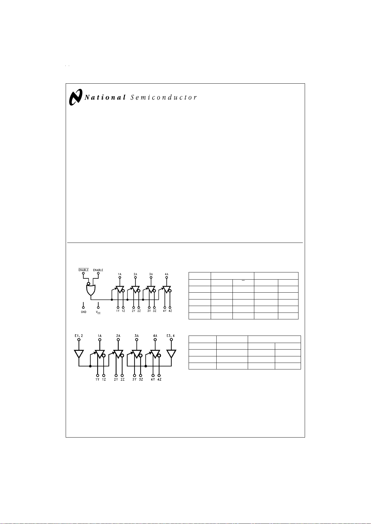
Logic Diagrams Function Tables (Each Driver)
DS96F172
Input Enable Outputs
AEE
YZ
HHXHL
LHXLH
HXLHL
LXLLH
XLHZZ
DS96F174
Input Enable Outputs
AEYZ
HHHL
LHLH
XLZZ
H = High Level
L = Low Level
X = Don’t Care
Z = High Impedance (Off)
TRI-STATE®is a registered trademark of National Semiconductor Corporation.
DS96F172
DS009625-14
DS96F174
DS009625-15
June 1998
DS96F172C/DS96F172M/DS96F174C/DS96F174M EIA-485/EIA-422 Quad Differential Drivers
© 1998 National Semiconductor Corporation DS009625 www.national.com
Page 2
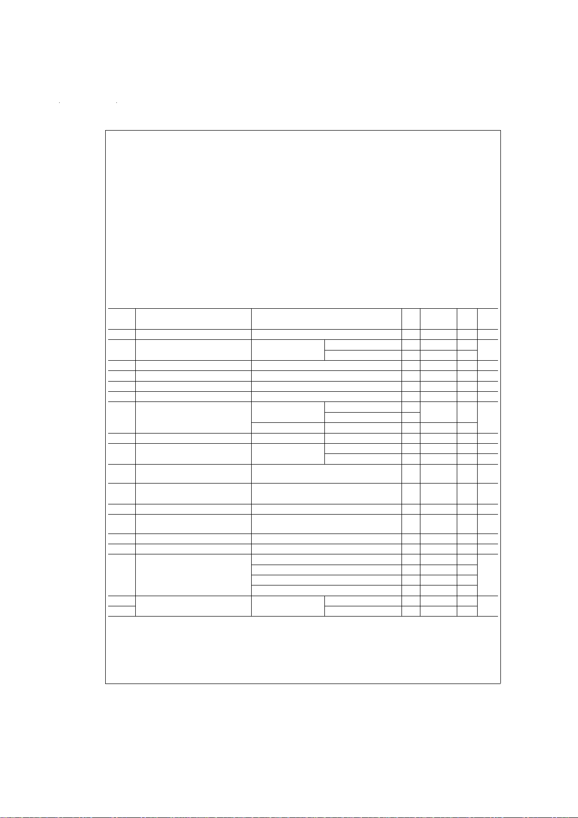
COMMERCIAL
Absolute Maximum Ratings
(Note 2)
Specifications for the 883 version of this product are
listed separately on the following pages.
Storage Temperature Range (T
STG
) −65˚C to +175˚C
Lead Temperature (Soldering, 60 sec.) 300˚C
Maximum Package Power Dissipation (Note 1) at 25˚C
Ceramic DIP (J) 1500 mW
Supply Voltage 7.0V
Enable Input Voltage 5.5V
Recommended Operating
Conditions
Min Typ Max Units
Supply Voltage (V
CC
)
DS96F172C/DS96F174C 4.75 5.0 5.25 V
Common Mode −7.0 +12.0 V
Output Voltage (V
OC
)
Output Current HIGH (I
OH
) −60 mA
Output Current LOW (I
OL
)60mA
Operating Temperature
(T
A
)
DS96F172C/DS96F174C 0 +70 ˚C
Note 1: Derate “J” package 10 mW/˚C above 25˚C.
Electrical Characteristics (Notes 3, 4)
Over recommended supply voltage and operating temperature range, unless otherwise specified
Symbol Parameter Conditions Min Typ Max Units
(Note 2)
V
IH
Input Voltage HIGH 2.0 V
V
IL
Input Voltage LOW TA= 0˚C to +70˚C 0.8 V
T
A
= −55˚C to +125˚C 0.7
V
OH
Output Voltage HIGH IOH= −33 mA TA= 0˚C to +70˚C 3.0 V
V
OL
Output Voltage LOW IOL=33mA TA= 0˚C to +70˚C 2.0 V
V
IC
Input Clamp Voltage II= −18 mA −1.5 V
|V
OD1
| Differential Output Voltage IO= 0 mA 6.0 V
|V
OD2
| Differential Output Voltage RL=54Ω,
Figure 1
TA= −55˚C 1.2 2.0 V
1.5
R
L
= 100Ω,
Figure 1
2.0 2.3
V
OD
Differential Output Voltage
Figure 2
TA= 0˚C to +70˚C 1.0 V
∆|V
OD
| Change in Magnitude of Differential RL=54Ωor 100Ω, −40˚C to +125˚C
±
0.2 V
Output Voltage (Note 5)
Figure 1
−55˚C to +125˚C
±
0.4 V
V
OC
Common Mode Output Voltage
(Note 6)
RL=54Ωor 100Ω,
Figure 1
3.0 V
∆|V
OC
| Change in Magnitude of Common RL=54Ωor 100Ω,
Figure 1
±
0.2 V
Mode Output Voltage (Note 5)
I
O
Output Current with Power Off VCC= 0V, VO= −7.0V to +12V
±
50 µA
I
OZ
High Impedance State Output
Current
VO= −7.0V to +12V
±
20
±
50 µA
I
IH
Input Current HIGH VI= 2.4V 20 µA
I
IL
Input Current LOW VI= 0.4V −50 µA
I
OS
Short Circuit Output Current VO= −7.0V −250
(Note 7) V
O
= 0V −150 mA
V
O=VCC
150
V
O
= +12V 250
I
CC
Supply Current (All Drivers) No Load Outputs Enabled 50 mA
I
CCX
Outputs Disabled 30
www.national.com 2
Page 3
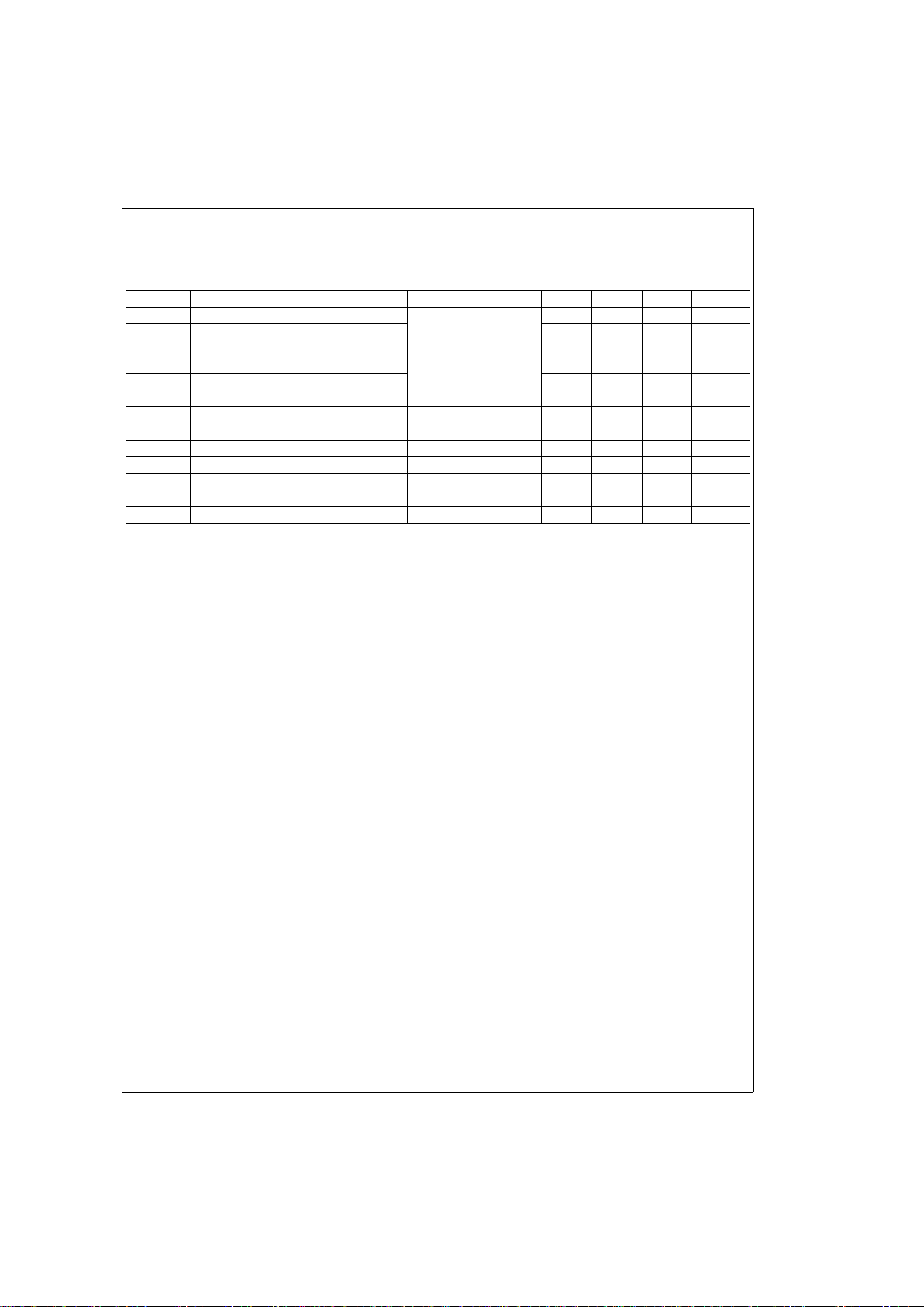
COMMERCIAL
Switching Characteristics
VCC= 5.0V, TA= 25˚C
Symbol Parameter Conditions Min Typ Max Units
t
DD
Differential Output Delay Time RL=60Ω,
Figure 3
15 20 ns
t
TD
Differential Output Transition Time 15 22 ns
t
PLH
Propagation Delay Time, RL=27Ω,
Figure 4
12 16 ns
Low-to-High Level Output
t
PHL
Propagation Delay Time, 12 16 ns
High-to-Low Level Output
t
ZH
Output Enable Time to High Level RL= 110Ω,
FIgure 4
25 32 ns
t
ZL
Output Enable Time to Low Level RL= 110Ω,
Figure 6
25 32 ns
t
HZ
Output Disable Time from High Level RL= 110Ω,
Figure 5
25 30 ns
t
LZ
Output Disable Time from Low Level RL= 110Ω,
Figure 6
20 25 ns
t
LZL
Output Disable Time from Low Level
Figure 6
300 ns
with Load Resistor to GND (Note 8)
t
SKEW
Driver Output to Output RL=60Ω 1.0 4.0 ns
Note 2: “Absolute Maximum Ratings” are those values beyond which the safety of the device cannot be guaranteed. They are not meant to imply that the devices
should be operated at these limits. The tables of “Electrical Characteristics” provide conditions for actual device operation.
Note 3: Unless otherwise specified min/max limits apply across the 0˚C to +70˚C range for the DS96F172C/DS96F174C. All typicals are given for V
CC
= 5V and T
A
= 25˚C.
Note 4: All currents into the device pins are positive; all currents out of the device pins are negative. All voltages are reference to ground unless otherwise specified.
Note 5: ∆|V
OD
| and ∆|VOC| are the changes in magnitude of VODand VOCrespectively, that occur when the input is changed from a high level to a low level.
Note 6: In EIA-422A and EIA-485 standards, VOC, which is the average of the two output voltages with respect to ground, is called output offset voltage, V
OS
.
Note 7: Only one output at a time should be shorted.
Note 8: For more information see Application Bulletin, contact Product Marketing.
Order Number: DS96F172CN
DS96F174CJ
DS96F174CN
NS Package Number J16A or N16E
www.national.com3
Page 4
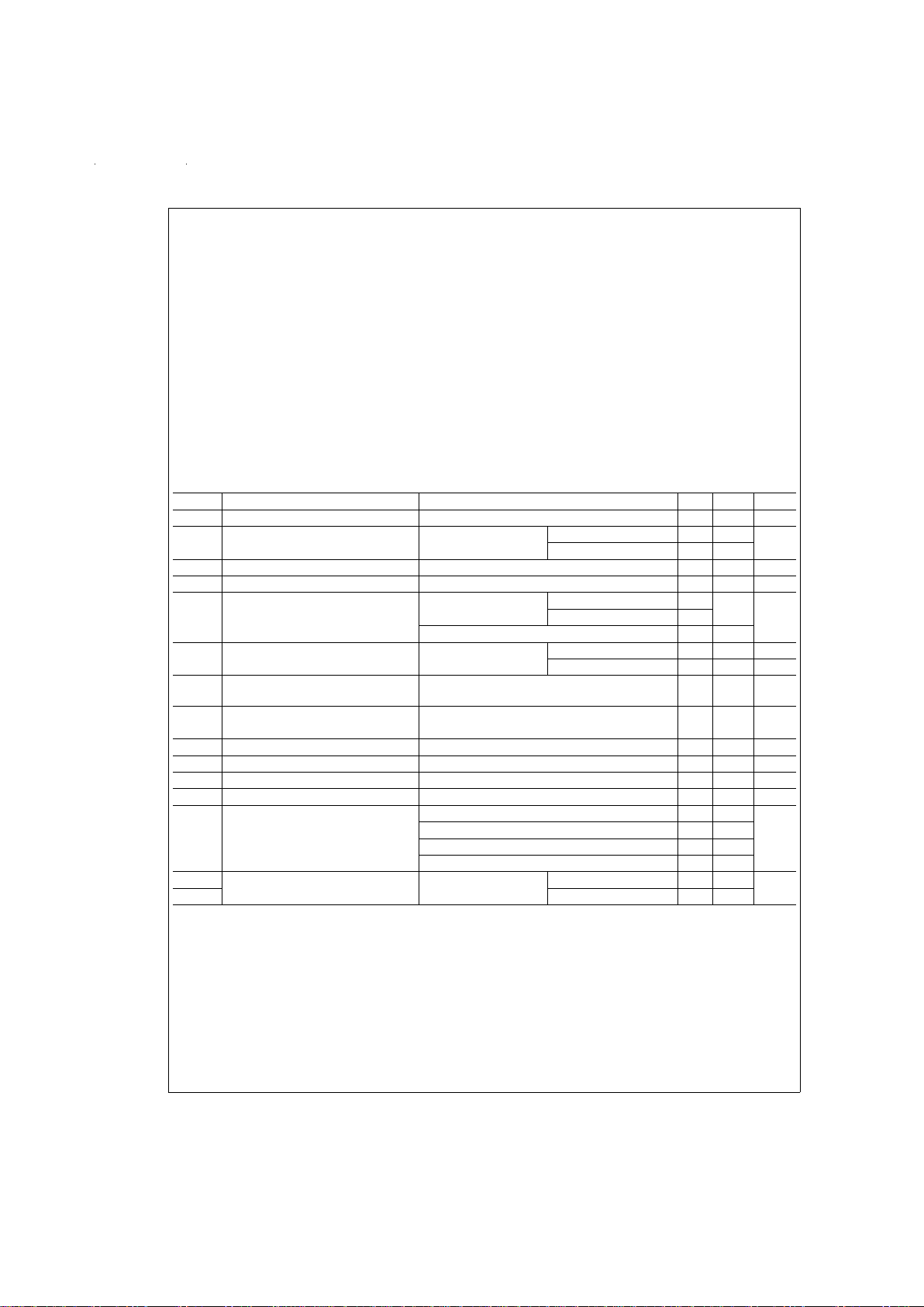
MIL-STD-883C
Absolute Maximum Ratings
(Note 2)
For complete Military Specifications, refer to the appropriate SMD or MDS.
Storage Temperature Range (T
STG
) −65˚C to +175˚C
Lead Temperature (Soldering, 60 sec.) 300˚C
Maximum Package Power Dissipation (Note 9) at 25˚C
Ceramic LCC (E) 2000 mW
Ceramic DIP (J) 1800 mW
Ceramic Flatpak (W) 1000 mW
Supply Voltage 7.0V
Enable Input Voltage 5.5V
Recommended Operating
Conditions
Min Typ Max Units
Supply Voltage (V
CC
)
DS96F172M/DS96F174M 4.50 5.0 5.50 V
Common Mode −7.0 +12.0 V
Output Voltage (V
OC
)
Output Current HIGH (I
OH
) −60 mA
Output Current LOW (I
OL
)60mA
Operating Temperature (T
A
)
DS96F172M/DS96F174M −55 +125
Note 9: Above TA= 25˚C, derate “E” package 13.4, “J” package 12.5, “W”
package 7.1 mW/˚C
Electrical Characteristics (Notes 3, 4)
Over recommended supply voltage and operating temperature range unless otherwise specified
Symbol Parameter Conditions Min Max Units
V
IH
Input Voltage HIGH 2.0 V
V
IL
Input Voltage LOW TA= 25˚C 0.8 V
T
A
= −55˚C, or +125˚C 0.7
V
IC
Input Clamp Voltage II= −18 mA −1.5 V
|V
OD1
| Differential Output Voltage IO= 0 mA 6.0 V
|V
OD2
| Differential Output Voltage RL=54Ω,VCC= 4.5V TA= −55˚C 1.2
Figure 1
TA= 25˚C, or +125˚C 1.5 V
R
L
= 100Ω,VCC= 4.5V,
Figure 1
2.0
∆|V
OD
| Change in Magnitude of Differential RL=54Ωor 100Ω,TA= 25˚C, or +125˚C
±
0.2 V
Output Voltage (Note 5) V
CC
= 4.5V,
Figure 1
−55˚C
±
0.4 V
V
OC
Common Mode Output Voltage
(Note 6)
RL=54Ωor 100Ω,
Figure 1
3.0 V
∆|V
OC
| Change in Magnitude of Common RL=54Ωor 100Ω,VCC= 4.5V,
Figure 1
±
0.2 V
Mode Output Voltage (Note 5)
I
O
Output Current with Power Off VCC= 0V, VO= −7.0V to +12V
±
50 µA
I
OZ
High Impedance State Output Current VO= −7.0V to +12V
±
50 µA
I
IH
Input Current HIGH VI= 2.4V 20 µA
I
IL
Input Current LOW VI= 0.4V −50 µA
I
OS
Short Circuit Output Current VO= −7.0V −250
(Note 7) V
O
= 0V −150 mA
V
O=VCC
150
V
O
= +12V 250
I
CC
Supply Current (All Drivers) No Load Outputs Enabled 50 mA
I
CCX
Outputs Disabled 30
www.national.com 4
Page 5

MIL-STD-883C
Switching Characteristics
VCC= 5.0V
Symbol Parameter Conditions T
A
= 25˚C TA= 55˚C TA= 125˚C Units
Typ Max Max Max
t
DD
Differential Output Delay Time RL=60Ω,CL= 15 pF, 15 22 30 30 ns
t
TD
Differential Output Transition Time
Figure 3
15 22 40 40 ns
t
PLH
Propagation Delay Time, RL=27Ω,CL= 15 pF, 12 16 25 25 ns
Low-to-High Level Output
Figure 4
t
PHL
Propagation Delay Time, 12 16 25 25 ns
High-to-Low Level Output
t
ZH
Output Enable Time to High Level RL= 110Ω,
Figure 5
25 32 40 40 ns
t
ZL
Output Enable Time to Low Level RL= 110Ω,
Figure 6
25 35 100 100 ns
t
HZ
Output Disable Time from High Level RL= 110Ω,
Figure 5,
25 30 80 80 ns
Note 13
t
LZ
Output Disable Time from Low Level RL= 110Ω,
Figure 6
20 25 40 40 ns
t
LZL
Output Disable Time from Low Level
Figure 6
300 ns
with Load Resistor to GND (Note 12)
t
SKEW
Driver Output to Output RL=60Ω 1.0 4.0 10 10 ns
SMD Numbers: DS96F172MJ/883 5962-9076501MEA
DS96F174MJ/883 5962-9076502MEA
DS96F172ME/883 5962-9076501M2A
DS96F174MW/883 5962-9076502MFA
DS96F174ME/883 5962-9076502M2A
Order Number: DS96F172MJ/883, DS96F174MJ/883
NS Package Number J16A
DS96F172ME/883, DS96F174ME/883
NS Package Number E20A
DS96F172MW-MIL, DS96F174MW/883
NS Package Number W16A
For Complete Military Product Specifications, refer to the appropriate SMD or MDS.
Parameter Measurement Information
DS009625-3
FIGURE 1. Differential and Common
Mode Output Voltage
DS009625-13
FIGURE 2. Differential Output Voltage with
Varying Common Mode Voltage
www.national.com5
Page 6

Parameter Measurement Information (Continued)
Note 10: The input pulse is supplied by a generator having the following characteristics: f = 1.0 MHz, duty cycle = 50%,tr≤5.0 ns, tf≤ 5.0 ns, ZO=50Ω.
Note 11: C
L
includes probe and jig capacitance.
Note 12: DS96F172 with active high and active low Enables is shown. DS96F174 has active high Enable only.
Note 13: To test the active low Enable E of DS96F172 ground E and apply an inverted waveform to E . DS96F174 has active high Enable only.
Note 14: For more information see Application Bulletin, Contact Product Marketing.
Note 15: Not tested for DS96F172MW-MIL device.
DS009625-4
DS009625-5
FIGURE 3. Differential Output Delay and Transition Times
DS009625-6
DS009625-7
FIGURE 4. Propagation Delay Times
DS009625-8
DS009625-9
FIGURE 5. tZHand t
HZ
DS009625-10
DS009625-11
FIGURE 6. tZL,tLZ,t
LZL
www.national.com 6
Page 7

Typical Application
Connection Diagrams
DS009625-12
The line length should be terminated at both ends in its characteristic impedance.
Stub lengths off the main line should be kept as short as possible.
16-Lead Ceramic Dual-In-Line Package
NS Package Number J16A
DS96F172
DS009625-1
Top View
DS96F174
DS009625-2
Top View
20-Lead Ceramic Leadless Chip Carrier
NS Package Number E20A
DS009625-18
NC = No connection
Top View
DS009625-19
Top View
www.national.com7
Page 8

Connection Diagrams (Continued)
16-Lead Ceramic Flatpak
NS Package Number W16A
DS009625-1
Top View
DS009625-2
Top View
Order Numbers are located at the end of the respective Electrical Tables.
www.national.com 8
Page 9

9
Page 10

Physical Dimensions inches (millimeters) unless otherwise noted
20-Lead Ceramic Leadless Chip Carrier (E)
Order Number DS96F172ME/883, DS96F174ME/883
NS Package Number E20A
16-Lead Ceramic Dual-In-Line Package (J)
Order Number DS96F172MJ/883,
DS96F174CJ, DS96F174MJ/883
NS Package Number J16A
www.national.com 10
Page 11

Physical Dimensions inches (millimeters) unless otherwise noted (Continued)
16-Lead Ceramic Flatpack (W)
Order Number DS96F172MW/883, DS96F174MW/883
NS Package Number W16A
Molded Dual-In-Line Package (N)
Order Number DS96F172CN, or DS96F174CN
NS Package Number N16E
www.national.com11
Page 12

LIFE SUPPORT POLICY
NATIONAL’S PRODUCTS ARE NOT AUTHORIZED FOR USE AS CRITICAL COMPONENTS IN LIFE SUPPORT DEVICES OR SYSTEMS WITHOUT THE EXPRESS WRITTEN APPROVAL OF THE PRESIDENT OF NATIONAL SEMICONDUCTOR CORPORATION. As used herein:
1. Life support devices or systems are devices or sys-
tems which, (a) are intended for surgical implant into
the body, or (b) support or sustain life, and whose failure to perform when properly used in accordance
with instructions for use provided in the labeling, can
be reasonably expected to result in a significant injury
to the user.
2. A critical component in any component of a life support
device or system whose failure to perform can be reasonably expected to cause the failure of the life support
device or system, or to affect its safety or effectiveness.
National Semiconductor
Corporation
Americas
Tel: 1-800-272-9959
Fax: 1-800-737-7018
Email: support@nsc.com
www.national.com
National Semiconductor
Europe
Fax: +49 (0) 1 80-530 85 86
Email: europe.support@nsc.com
Deutsch Tel: +49 (0) 1 80-530 85 85
English Tel: +49 (0) 1 80-532 78 32
Français Tel: +49 (0) 1 80-532 93 58
Italiano Tel: +49 (0) 1 80-534 16 80
National Semiconductor
Asia Pacific Customer
Response Group
Tel: 65-2544466
Fax: 65-2504466
Email: sea.support@nsc.com
National Semiconductor
Japan Ltd.
Tel: 81-3-5620-6175
Fax: 81-3-5620-6179
DS96F172C/DS96F172M/DS96F174C/DS96F174M EIA-485/EIA-422 Quad Differential Drivers
National does not assume any responsibility for use of any circuitry described, no circuit patent licenses are implied and National reserves the right at any time without notice to change said circuitry and specifications.
 Loading...