

Page 1
DS9637A
Dual Differential Line Receiver
General Description
The DS9637A is a Schottky dual differential line receiver
which has been specifically designed to satisfy the requirements ofEIAStandards RS-422 and RS-423. In addition, the
DS9637A satisfies the requirements of MIL-STD 188-114
and is compatible with the International Standard CCITT recommendations. The DS9637Ais suitable for use as a line receiver in digital data systems, using either single ended or
differential, unipolar or bipolar transmission. It requires a
single 5V power supply and has Schottky TTL compatible
outputs. The DS9637A has an operational input common
mode range of
±
7V either differentially or to ground.
Features
n Dual channel
n Single 5V supply
n Satisfies EIA standards RS-422 and RS423
n Built-in
±
35 mV hysteresis
n High input common mode voltage range
n High input impedance
n TTL compatible outputs
n Schottky technology
n Extended temperature range
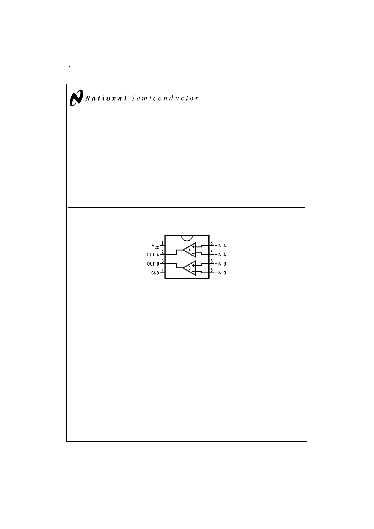
Connection Diagram
8–Lead DIP and SO-8 Package
DS009621-1
Top View
Order Number DS9637ACM or DS9637ACN
See NS Package Number M08A or N08E
For Complete Military Product Specifications,
refer to the appropriate SMD or MDS.
Order Number DS9637AMJ/883
See NS Package Number J08A
May 1998
DS9637A Dual Differential Line Receiver
© 1998 National Semiconductor Corporation DS009621 www.national.com
Page 2
Absolute Maximum Ratings (Note 2)
If Military/Aerospace specified devices are required,
please contact the National Semiconductor Sales Office/
Distributors for availability and specifications.
Storage Temperature Range
Ceramic DIP −65˚C to + 175˚C
Molded DIP −65˚C to + 150˚C
Lead Temperature
Ceramic DIP
(Soldering, 30 seconds) 300˚C
Molded DIP and SO Package
(Soldering, 10 seconds) 265˚C
Maximum Power Dissipation (Note 1) at 25˚C
Cavity Package 1300 mW
Molded Package 930 mW
SO Package 810 mW
V
CC
Lead Potential to Ground −0.5V to 7.0V
Input Potential to Ground
±
15V
Differential Input Voltage
±
15V
Output Potential to Ground −0.5V to +5.5V
Output Sink Current 50 mA
Recommended Operating
Conditions
DS9637AM Min Max Units
Supply Voltage (V
CC
) 4.5 5.5 V
Operating Temperature (T
A
) −55 +125 ˚C
DS9637AC
Supply Voltage (V
CC
) 4.75 5.25 V
Operating Temperature (T
A
) 0 +70 ˚C
Note 1: Derate cavity package 8.7 mW/˚C above 25˚C; derate molded DIP
package 7.5 mW/˚C above 25˚C; derate SO package 6.5 mW/˚C above 25˚C.
Electrical Characteristics (Notes 3, 4)
Over recommended operating temperature and supply voltage ranges, unless otherwise specified
Symbol Parameter Conditions Min Typ Max Units
V
TH
Differential Input −7.0V ≤ VCM≤ +7.0V −0.2 +0.2 V
Threshold Voltage (Note 6)
V
TH(R)
Differential Input −7.0V ≤ VCM≤ +7.0V −0.4 +0.4 V
Threshold Voltage (Note 7)
I
I
Input Current V
I
=
10V, 0V ≤ V
CC
≤ +5.5V 1.1 3.25 mA
(Note 8) V
I
=
−10V, 0V ≤ V
CC
≤ +5.5V −1.6 −3.25
V
OL
Output Voltage LOW I
OL
=
20 mA, V
CC
=
Min 0.35 0.5 V
V
OH
Output Voltage HIGH I
OH
=
−1.0 mA, V
CC
=
Min 2.5 3.5 V
I
OS
Output Short Circuit V
O
=
0V, V
CC
=
Max −40 −75 −100 mA
Current (Note 5)
I
CC
Supply Current V
CC
=
Max, V
I
+=0.5V, 35 50 mA
V
I
−=GND
V
HYST
Input Hysteresis V
CM
=
±
7.0V (See Curves) 70 mV
Note 2: “Absolute Maximum Ratings” are those values beyond which the safety of the device cannot be guaranteed. They are not meant to imply that the devices
should be operated at these limits. The tables of “Electrical Characteristics” provide conditions for actual device operation.
Note 3: Unless otherwise specified Min/Max limits apply across the −55˚C to +125˚C temperature range for DS9637AM and across the 0˚C to +70˚C range for the
DS9637ASC. All typicals are given for V
CC
=
5V and T
A
=
25˚C.
Note 4: All currents into the device pins are positive; all currents out of the device pins are negative.Allvoltagesarereferenced to ground unless otherwise specified.
Note 5: Only one output at a time should be shorted.
Note 6: V
DIFF
(Differential Input Voltage)=(VI+)−(VI−). VCM(Common Mode Input Voltage)=VI+orVI−.
Note 7: 500Ω
±
1%in series with inputs.
Note 8: The input not under test is tied to ground.
Switching Characteristics
V
CC
=
5.0V, T
A
=
25˚C
Symbol Parameter Conditions Min Typ Max Units
t
PLH
Propagation Delay Time See AC Test Circuit 15 25 ns
Low to High
t
PHL
Propagation Delay Time See AC Test Circuit 13 25 ns
High to Low
www.national.com 2
Page 3

Switching Characteristics (Continued)
Typical Input/Output Transfer Characteristics
DS009621-2
FIGURE 1. Equivalent Circuit
DS009621-3 DS009621-4
www.national.com3
Page 4

AC Test Circuit and Waveforms
Typical Applications
DS009621-5
Notes:
C
L
includes jig and probe capacitance.
All diodes are FD700 or equivalent.
FIGURE 2.
DS009621-6
V
I
Amplitude: 1.0V
Offset: 0.5V
Pulse Width: 100 ns
PRR: 5.0 MHz
t
r
=
t
f
≤ 5.0 ns
FIGURE 3.
DS009621-7
Notes:
R
T
≥ 50Ω for RS-422 operation.
R
T
combined with input impedance of receivers must be greater than 90Ω.
FIGURE 4. RS-422 System Application (FIPS 1020) Differential Simplex Bus Transmission
www.national.com 4
Page 5

Physical Dimensions inches (millimeters) unless otherwise noted
Ceramic Dual-In-Line Package (J)
Order Number DS9637AMJ/883
NS Package Number J08A
Molded Surface Mount Package (M)
Order Number DS9637ACM
NS Package Number M08A
www.national.com5
Page 6

Physical Dimensions inches (millimeters) unless otherwise noted (Continued)
LIFE SUPPORT POLICY
NATIONAL’S PRODUCTS ARE NOT AUTHORIZED FOR USE AS CRITICAL COMPONENTS IN LIFE SUPPORT DEVICES OR SYSTEMS WITHOUT THE EXPRESS WRITTEN APPROVAL OF THE PRESIDENT OF NATIONAL SEMICONDUCTOR CORPORATION. As used herein:
1. Life support devices or systems are devices or systems which, (a) are intended for surgical implant into
the body, or (b) support or sustain life, and whose failure to perform when properly used in accordance
with instructions for use provided in the labeling, can
be reasonably expected to result in a significant injury
to the user.
2. A critical component in any component of a life support
device or system whose failure to perform can be reasonably expected to cause the failure of the life support
device or system, or to affect its safety or effectiveness.
National Semiconductor
Corporation
Americas
Tel: 1-800-272-9959
Fax: 1-800-737-7018
Email: support@nsc.com
www.national.com
National Semiconductor
Europe
Fax: +49 (0) 1 80-530 85 86
Email: europe.support@nsc.com
Deutsch Tel: +49 (0) 1 80-530 85 85
English Tel: +49 (0) 1 80-532 78 32
Français Tel: +49 (0) 1 80-532 93 58
Italiano Tel: +49 (0) 1 80-534 16 80
National Semiconductor
Asia Pacific Customer
Response Group
Tel: 65-2544466
Fax: 65-2504466
Email: sea.support@nsc.com
National Semiconductor
Japan Ltd.
Tel: 81-3-5620-6175
Fax: 81-3-5620-6179
Molded Dual-In-Line Package (N)
Order Number DS9637ACN
NS Package Number N08E
DS9637A Dual Differential Line Receiver
National does not assume any responsibility for use of any circuitry described, no circuit patent licenses are implied and National reserves the right at any time without notice to change said circuitry and specifications.
 Loading...