

Page 1
1 of 3 102199
SPECIAL FEATURES
§ Zener characteristic with voltage snap–back
to protect against ESD hits
§ High avalanche voltage, low leakage and low
capacitance avoid signal attenuation
§ Compatible to all 5V logic families
§ Space saving, low inductance TSOC surface
mount package
§ On–chip 5Ω resistors for isolation at both
anode and cathode terminals
§ Industrial temperature range
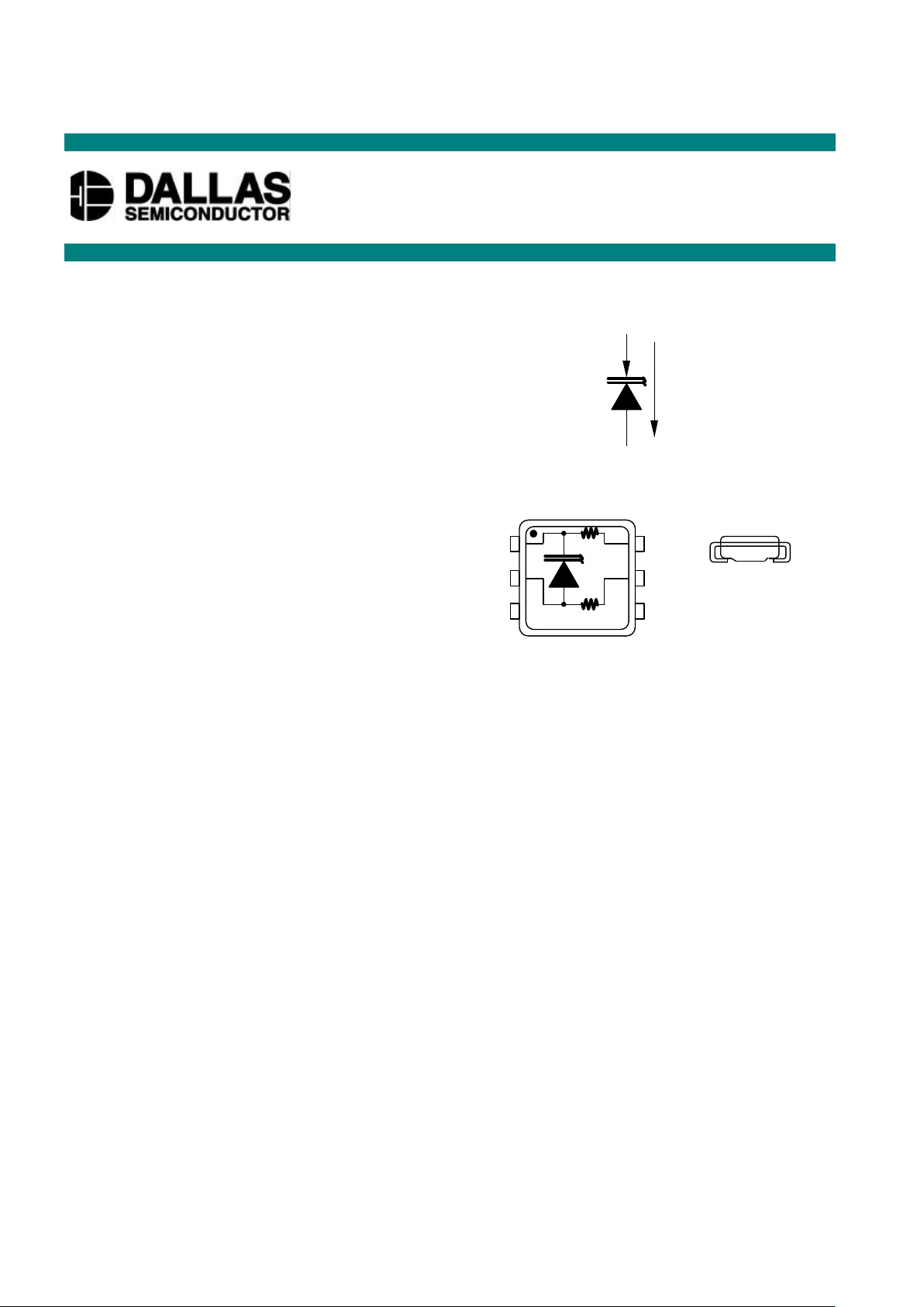
SYMBOL AND CONVENTIONS
PACKAGE OUTLINE
ORDERING INFORMATION
DS9503P 6-lead TSOC package
DESCRIPTION
This DS9503 is designed as an ESD protection device for 1–Wire MicroLAN interfaces. In contrast to the
DS9502, the DS9503 includes two 5Ω isolation resistors on chip. Although 5Ω are negligible during
communication, they represent a high impedance relative to the conducting diode during an ESD event.
Thus, the diode absorbs the energy while the resistors further isolate and protect the circuit at the other
side of the package. If used with circuits that already have a strong ESD–protection at their I/O port, the
ESD protection level is raised to more that 27 kV (IEC 801–2 Reference model). In case of abnormal
ESD hits beyond its maximum ratings the DS9503 will eventually fail “short” thus preventing further
damage.
During normal operation the DS9503 behaves like a regular 7.5V Zener Diode. When the voltage
exceeds the trigger voltage, the I/V characteristic of the device will “snapback” allowing the same or
higher amount of current to flow, but at a significantly lower voltage. As long as a minimum current or
voltage is maintained, the device will stay in the “snapback mode”. If the voltage or the current falls
below the holding voltage or holding current, the device will abruptly change to its normal mode and
conduct only a small leakage current.
VCA
A
IC
C
TSOC SURFACE MOUNT PACKAGE
3.7 X 4.0 X 1.5 mm
See Mech. Drawings
Section
61
52
43
TOP VIEW
DS9503
ESD Protection Diode with Resistors
www.dalsemi.com
SIDE VIEW
Page 2
DS9503
2 of 3 102199
DC CHARACTERISTICS Figure 1
DC CHARACTERISTICS DETAIL DRAWING Figure 2
TEST PULSE WAVEFORM Figure 3
TYPICAL APPLICATION Figure 4
Page 3

DS9503
3 of 3 102199
PHYSICAL SPECIFICATIONS
Size See mechanical drawing
Weight 0.5 grams
ABSOLUTE MAXIMUM RATINGS*
Operating Temperature –40°C to +85°C
Storage Temperature –55°C to +125°C
Soldering Temperature 260°C for 10 seconds
Continuous DC Current Through Package 80 mA
∗ This is a stress rating only and functional operation of the device at these or any other conditions
above those indicated in the operation sections of this specification is not implied. Exposure to
absolute maximum rating conditions for extended periods of time may affect reliability
ELECTRICAL CHARACTERISTICS (-40°C to +85°C)
PARAMETER SYMBOL MIN TYP MAX UNITS NOTES
Leakage Current I
L
30 100 nA 2
Avalanche Voltage V
AV
7.4 7.8 V 1,3
Trigger Voltage V
TRIGGER
9.0 9.5 V 1
Trigger Current I
TRIGGER
600 1000 mA
Holding Voltage V
HOLD
5.5 V 1
Holding Current I
HOLD
30 mA
Forward Voltage (-10 mA) V
F
-0.7 -0.8 V 4
Forward Current (-0.7V) I
F
-10 -100 mA 4
Maximum Peak Current I
PP
2.0 A 5
Continuous Current Through Diode I
CC
±80
mA
Isolation Resistance R
I
5
Ω
CAPACITANCE (tA=25°C)
PARAMETER SYMBOL MIN TYP MAX UNITS NOTES
Junction Capacitance (5V) C
J5
40 pF 1
Junction Capacitance (0V) C
J0
70 pF 1
THERMAL RESISTANCE
PARAMETER SYMBOL MIN TYP MAX UNITS NOTES
Junction To Package
R
ΘJC
75 K/W
Junction To Ambient
R
ΘJA
200 K/W
NOTES:
1. All voltages are referenced from Cathode to Anode.
2. At 7.0V.
3. At 0.3 µA.
4. Typical values at room temperature.
5. See pulse specification.
 Loading...