

Page 1
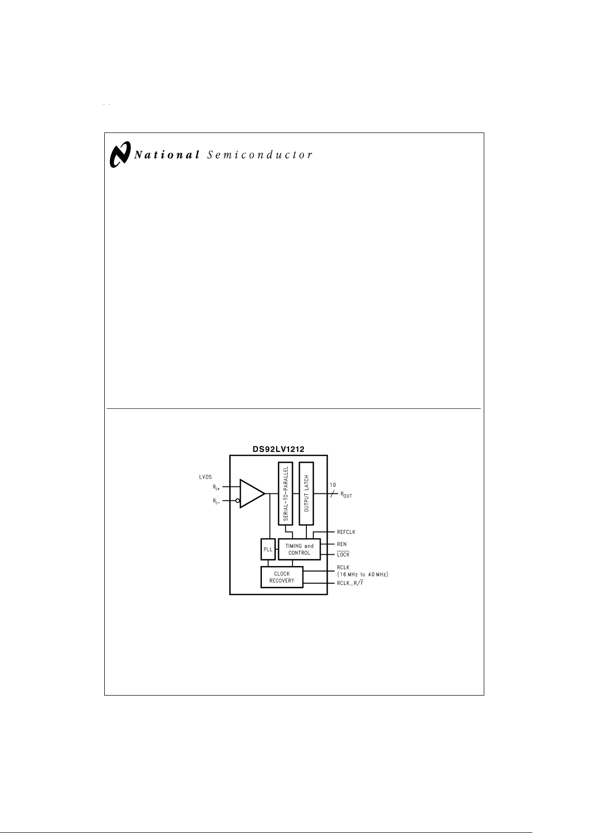
DS92LV1212
16-40 MHz 10-Bit Bus LVDS Random Lock Deserializer
with Embedded Clock Recovery
General Description
The DS92LV1212 is an upgrade of the DS92LV1210. It
maintains all of the features of the DS92LV1210withtheadditional capability of locking to the incoming data stream
without the need of SYNC patterns. This makes the
DS92LV1212 useful in applications where the Deserializer
must be operated “open-loop”—without a feedback path
from the Deserializer to the Serializer. The DS92LV1212 is
designed to be used with the DS92LV1021 Bus LVDSSerializer. The DS92LV1212 receives a Bus LVDS serial data
stream and transforms it into a 10-bit wide parallel data bus
and separate clock. The reduced cable, PCB trace count
and connector size saves cost and makes PCB layout
easier. Clock-to-data and data-to-data skews are eliminated
since one input receives both clock and data bits serially.
The powerdown pin is used to save power by reducing the
supply current when the device is not in use. The Deserializer will establish lock to a synchronization pattern within
specified lock times but it can also lock to a data stream without SYNC patterns.
Features
n Clock recovery without SYNC patterns-random lock
n Guaranteed transition every data transfer cycle
n Chipset (Tx + Rx) power consumption
<
300mW (typ)
@
40MHz
n Single differential pair eliminates multi-channel skew
n 400 Mbps serial Bus LVDS bandwidth (at 40 MHz clock)
n 10-bit parallel interface for 1 byte data plus 2 control bits
or UTOPIA I Interface
n Synchronization mode and LOCK indicator
n Flow-through pinout for easy PCB layout
n High impedance on receiver inputs when power is off
n Programmable edge trigger on clock
n Footprint compatible with DS92LV1210
n Small 28-lead SSOP package-MSA
Block Diagram
TRI-STATE®is a registered trademark of National Semiconductor Corporation.
DS100982-1
April 1999
DS92LV1212 16-40 MHz 10-Bit Bus LVDS Random Lock Deserializer with Embedded Clock
Recovery
© 1999 National Semiconductor Corporation DS100982 www.national.com
Page 2
Block Diagram (Continued)
Functional Description
The DS92LV1212 is a 10-bit Deserializer chip designed to
receive data over a heavily loaded differential backplanes at
clock speeds from 16 MHz to 40 MHz. It may also be used to
receive data over Unshielded Twisted Pair (UTP) cable.
The chip has three active states of operation: Initialization,
Data Transfer, and Resynchronization; and two passive
states: Powerdown and TRI-STATE
®
.
The following sections describe each operation and passive
state.
Initialization
Before data can be transferred the Deserializer must be initialized. The Deserializer should be powered up with the
PWRDN pin held low. After V
CC
stabilizes the PWRDN pin
can be forced high. The Deserializer is ready to lock to the
incoming data stream.
Step 1: When V
CC
is applied to the Deserializer, the respective outputs are held in TRI-STATE and internal circuitry is
disabled by on-chip power-on circuitry. When V
CC
reaches
V
CC
OK (2.5V) the PLL is ready to lock to incoming data or
synchronization patterns. The local clock is applied to the
REFCLK pin.
The Deserializer LOCK output will remain high while its PLL
is locking to the incoming data or to SYNC patterns on the input.
Step 2: The Deserializer PLL must synchronize to the Serializer to complete the initialization. The Deserializer will lock to
non-repetitive data patterns, however, the transmission of
SYNC patterns to the Deserializer enables the Deserializer
to lock to the Serializer signal within a specified time.
Control of the Serializer SYNC1/2 pins is left to the user. A
feedback loop between the LOCK pin is one recommendation. Another option is that one or both of the Serializer
SYNC inputs are asserted for at least 1024 cycles of TCLK
to initiate transmission of SYNC patterns. The Serializer will
continue to send SYNC patterns after the minimum of 1024
if either of the SYNC inputs remain high.
When the Deserializer detects edge transitions at the Bus
LVDS input it will attempt to lock to the embedded clock in-
formation. When the Deserializer locks to the Bus LVDS
clock, the LOCK output will go low. When LOCK is low the
Deserializer outputs represent incoming Bus LVDS data.
Data Transfer
Serialized data and clock bits (10+2 bits) are received at 12
times the TCLK frequency. For example, if TCLK is 40 MHz,
the serial rate is 40 x 12 = 480 Mega bits per second. Since
only 10 bits are from input data, the serial “payload” rate is
10 times the TCLK frequency. For instance, if TCLK = 40
MHz, the payload data rate is 40 x 10 = 400 Mbps. TCLK is
provided by the data source and must be in the range 16
MHz to 40 MHz nominal.
The LOCK pin on the Deserializer is driven low when it is
synchronized with the Serializer. The Deserializer locks to
the embedded clock and uses it to recover the serialized
data. ROUT data is valid when LOCK is low. Otherwise
ROUT0–ROUT9 is invalid.
RCLK pin is the reference to data on the ROUT0-ROUT9
pins. The polarity of the RCLK edge is controlled by the
RCLK_R/F input.
ROUT(0-9), LOCK and RCLK outputs will drive a minimum
of three CMOS input gates (15 pF load) with 40 MHz clock.
Resynchronization
The Deserializer LOCK pin driven low indicates that the Deserializer PLL is locked to the embedded clock edge. If the
Deserializer loses lock, the LOCK output will go high and the
outputs (including RCLK) will be TRI-STATE.
The LOCK pin must be monitored by the system to detect a
loss of synchronization. The system can arrange to pulse the
Serializer SYNC1 or SYNC2 pin to resynchronize. There are
multiple approaches possible. One recommendation is to
provide a feedback loop using the LOCK pin itself to control
the sync request of the Serializer (SYNC1 or SYNC2). A
minimum of 1024 sync patterns are needed to resynchronize. Dual SYNC pins are provided for multiple control in a
multi-drop application.
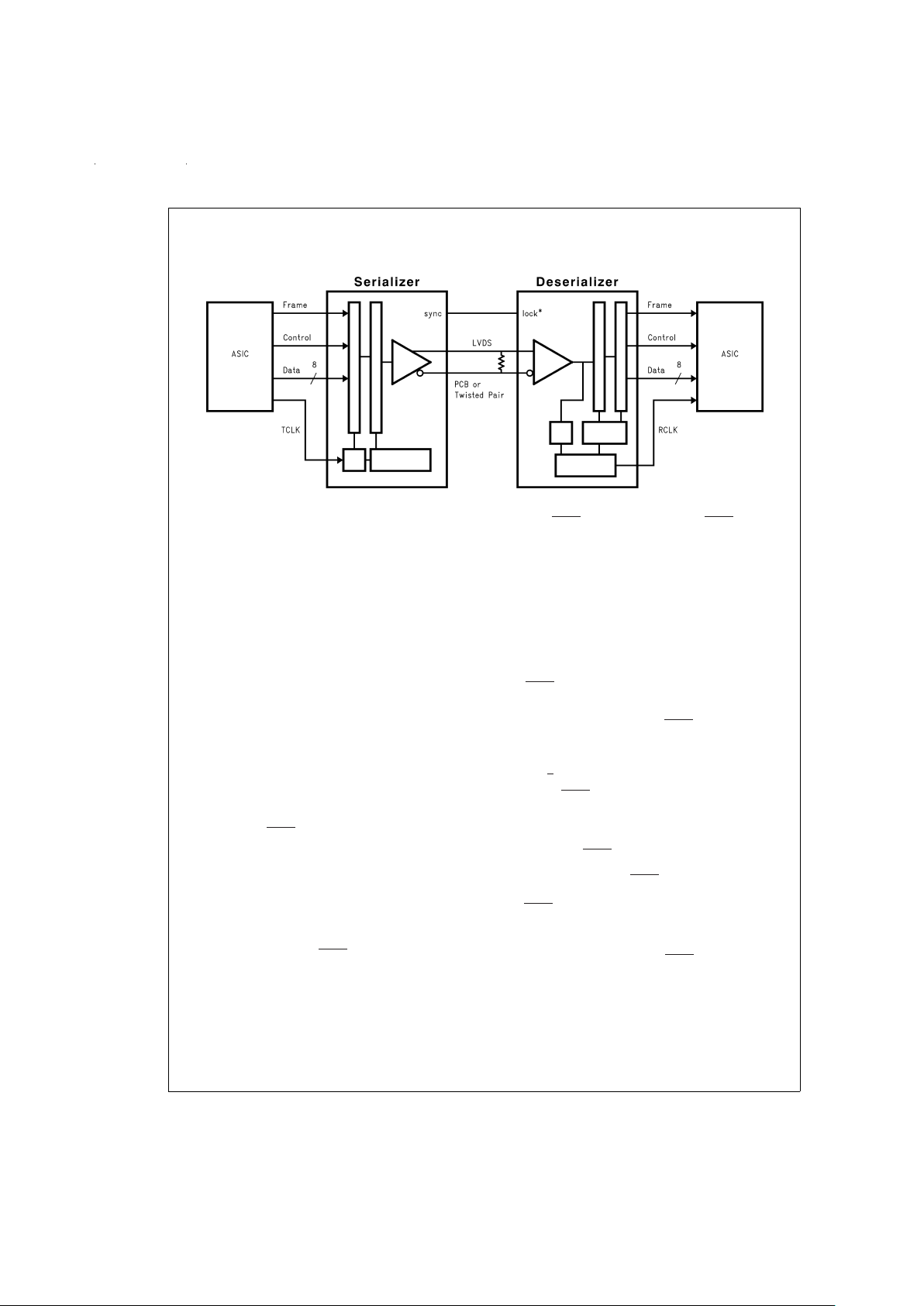
Application
DS100982-2
www.national.com 2
Page 3

Random Lock Initialization and
Resynchronization
The initialization and resynchronization methods described
in their respective sections are the fastest ways to establish
the link between the Serializer and Deserializer, however,
the DS92LV1212can attain lock to a data stream without requiring special SYNC patterns to be sent by the Serializer.
This allows the DS92LV1212 to be used in applications
where the Deserializer must operate “open-loop” and supports hot insertion into a running backplane. Because the
data stream is essentially random the time for the
DS92LV1212 to attain lock is variable and cannot be predicted. The primary constraint on the “random” lock time is
the initial phase relation when the Deserializer is powered
up. The data contained in the data stream can also affect
lock time. Typical lock times for random data have a mean of
570us and a max of 4.9ms.
If a specific pattern is repetitive the Deserializer could be
misled into a “false lock” - falsely recognizing the data pattern as the clocking bits. We refer to such a pattern as a repetitive multi-transition, RMT.Thisis when there is more than
one Low-High transition in a single clock cycle. This occurs
when any bit, except DIN 9, is held at a low state and the adjacent bit is held high creating a 0-1 transition. In the worst
case the Deserializer could become locked to the data pattern rather than the clock. Circuitry within the DS92LV1212
can detect that the possibility of “false lock” exists (by detecting that there is more than 1 potential position for clocking
bits) and will prevent the LOCK* output from becoming active until the potential “false lock” pattern changes. It is expected that the data will eventually change causing the Deserializer to lose lock to the data pattern and continue
searching for the clock bits in the serial data stream. A
graphical representation of a few cases of RMT is shown
below. Please note that RMT applies to bits DIN0-DIN8.
Powerdown
The Powerdown state is a low power sleep mode that can be
used to reduce power when there is no data to be transferred. Powerdown is entered when PWRDN and REN are
driven low on the Deserializer. In Powerdown, the PLL is
stopped and the outputs go into TRI-STATE, disabling load
current and also reducing supply current to the milliamp
range. To exit Powerdown, PWRDN is driven high.
Both the Serializer and Deserializer must re-initialize and resynchronize before data can be transferred. Initialization of
the Serializer takes 1024 TCLK cycles. The Deserializer will
initialize and assert LOCK high until it is locked to the Bus
LVDS clock.
TRI-STATE
For the Deserializer, TRI-STATE is entered when the REN
pin is driven low. This will TRI-STATE the receiver output
pins (ROUT0–ROUT9), LOCK and RCLK.
www.national.com3
Page 4
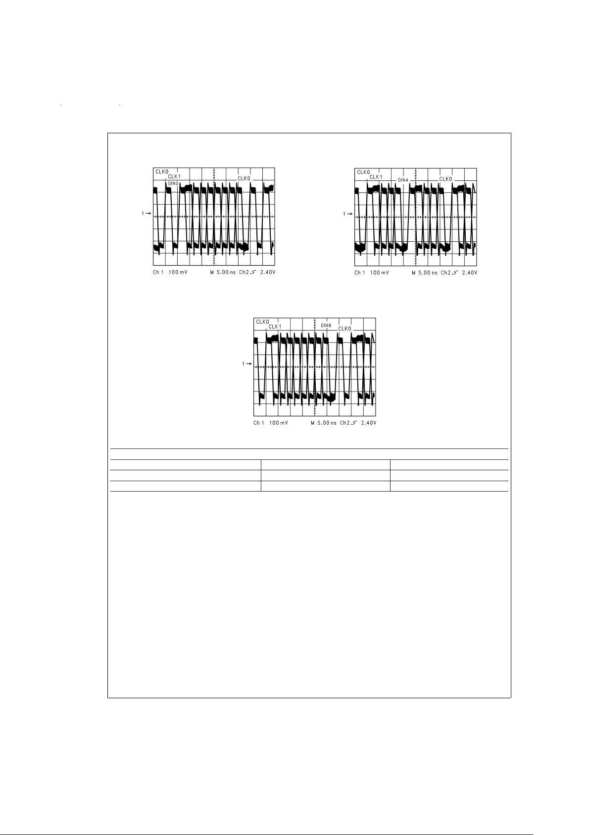
RMT Patterns
Order Numbers
NSID Function Package
DS92LV1021TMSA Serializer MSA28
DS92LV1212TMSA Deserializer MSA28
DS100982-23
DIN0 Held Low-DIN1 Held High Creates an RMT Pattern
DS100982-24
DIN4 Held Low-DIN5 Held High Creates an RMT Pattern
DS100982-25
DIN8 Held Low-DIN9 Held High Creates an RMT Pattern
www.national.com 4
Page 5

Absolute Maximum Ratings (Note 1)
If Military/Aerospace specified devices are required,
please contact the National Semiconductor Sales Office/
Distributors for availability and specifications.
Supply Voltage (V
CC
) −0.3V to +4V
CMOS/TTL Input Voltage −0.3V to (V
CC
+0.3V)
CMOS/TTL Output Voltage −0.3V to (V
CC
+0.3V)
Bus LVDS Receiver Input
Voltage −0.3V to +3.9V
Junction Temperature +150˚C
Storage Temperature −65˚C to +150˚C
Lead Temperature
(Soldering, 4 seconds) +260˚C
Maximum Package Power Dissipation Capacity
@
25˚C Package:
28L SSOP 1.27 W
Package Derating:
28L SSOP 10.2 mW/˚C above +25˚C
ESD Rating (HBM)
>
2.5kV
Recommended Operating
Conditions
Min Nom Max Units
Supply Voltage (V
CC
) 3.0 3.3 3.6 V
Operating Free Air
Temperature (T
A
)
−40 +25 +85 ˚C
Receiver Input Range 0 2.4 V
Supply Noise Voltage
(V
CC
)
100 mV
P-P
Electrical Characteristics
Over recommended operating supply and temperature ranges unless otherwise specified.
Symbol Parameter Conditions Min Typ Max Units
DESERIALIZER CMOS/TTL DC SPECIFICATIONS (apply to pins PWRDN, RCLK_R/ F, REN, REFCLK = inputs; apply to pins
ROUT, RCLK, LOCK = outputs)
V
IH
High Level Input Voltage 2.0 V
CC
V
V
IL
Low Level Input Voltage GND 0.8 V
V
CL
Input Clamp Voltage ICL= −18 mA −0.62 −1.5 V
I
IN
Input Current VIN= 0V or 3.6V −10
±
2 +10 µA
V
OH
High Level Output Voltage IOH= −9 mA 2.1 2.93 V
CC
V
V
OL
Low Level Output Voltage IOL= 9 mA GND 0.33 0.6 V
I
OS
Output Short Circuit Current VOUT = 0V −15 −38 −85 mA
I
OZ
TRI-STATE Output Current PWRDN or REN = 0.8V, V
OUT
=0VorVCC −10
±
0.4 +10 µA
DESERIALIZER Bus LVDS DC SPECIFICATIONS (apply to pins RI+ and RI−)
VTH Differential Threshold High
Voltage
VCM = +1.1V
+6 +100 mV
VTL Differential Threshold Low
Voltage
−100 −12 mV
I
IN
Input Current VIN= +2.4V, VCC= 3.6V or 0V −10
±
5 +10 µA
V
IN
= 0V, VCC= 3.6V or 0V −10
±
5 +10 µA
DESERIALIZER SUPPLY CURRENT (apply to pins DVCC and AVCC)
I
CCR
Deserializer Supply Current CL= 15 pF f = 40 MHz 47 60 mA
Worst Case
Figure 1
f = 16 MHz 30 40 mA
I
CCXR
Deserializer Supply Current
Powerdown
PWRDN = 0.8V, REN = 0.8V
0.34 1.0 mA
Deserializer Timing Requirements for REFCLK
Over recommended operating supply and temperature ranges unless otherwise specified.
Symbol Parameter Conditions Min Typ Max Units
t
RFCP
REFCLK Period 25 T 62.5 ns
t
RFDC
REFCLK Duty Cycle 50
%
f
Ref
REFCLK Frequency 0.95/t
RCP
t
RCP
1.05/t
RCP
t
RFTT
REFCLK Transition Time 3 6 ns
www.national.com5
Page 6

Deserializer Switching Characteristics
Over recommended operating supply and temperature ranges unless otherwise specified.
Symbol Parameter Conditions Pin/Freq. Min Typ Max Units
t
RCP
Receiver out Clock
Period
Figure 3
t
RCP=tTCP
RCLK
25 62.5 ns
t
CLH
CMOS/TTL Low-to-High
Transition Time
CL=15pF
Figure 2
Rout(0-9),
26ns
t
CHL
CMOS/TTL High-to-Low
Transition Time
LOCK, RCLK
26ns
t
DD
Deserializer Delay
Figure 4
1.75*t
RCP
+ 1.5 1.75*t
RCP
+4.0 1.75*t
RCP
+6.5 ns
t
ROS
ROUT (0-9) Setup Data to
RCLK
Figure 5
RCLK
0.4*t
RCP
0.5*t
RCP
ns
t
ROH
ROUT (0-9) Hold Data to
RCLK
−0.4*t
RCP
−0.5*t
RCP
ns
t
RDC
RCLK Duty Cycle 40 50 60
%
t
HZR
HIGH to TRI-STATE Delay
Figure 6
Rout(0-9),
LOCK
4.2+0.5*t
RCP
10+t
RCP
ns
t
LZR
LOW to TRI-STATE Delay 4.5+0.5*t
RCP
10+t
RCP
ns
t
ZHR
TRI-STATE to HIGH Delay 6+0.5*t
RCP
12+t
RCP
ns
t
ZLR
TRI-STATE to LOW Delay 6.0+0.5*t
RCP
12+t
RCP
ns
t
DSR1
Deserializer PLL Lock Time
from PWRDWN (with
SYNCPAT)
(Note 4)
Figure 7
Figure 8
16MHz
18.2 22 µs
40MHz
7.4 25.6 µs
t
DSR2
Deserializer PLL Lock time
from SYNCPAT
16MHz 21.0 30 µs
40MHz 14.4 25 µs
t
ZHLK
TRI-STATE to HIGH Delay
(power-up)
LOCK
4.62 12 ns
t
RNM
Deserializer Noise Margin
Figure 9
(Note 5)
16 MHz 400 1100 ps
40 MHz 100 400 ps
Note 1: “Absolute Maximum Ratings” are those values beyond which the safety of the device cannot be guaranteed. They are not meant to imply that the devices
should be operated at these limits. The table of “Electrical Characteristics” specifies conditions of device operation.
Note 2: Typical values are given for V
CC
= 3.3V and TA= +25˚C.
Note 3: Current into device pins is defined as positive. Current out of device pins is defined as negative. Voltages are referenced to ground except VOD, ∆VOD, VTH
and VTL which are differential voltages.
Note 4: For the purpose of specifying Deserializer PLL performance tDSR1 and tDSR2 are specified with the REFCLK running and stable, and specific conditions
of the incoming data stream (SYNCPATs).It is recommended that the Deserializer be initialized using either tDSR1 timing or tDSR2 timing. tDSR1 is the time required
for the Deserializer to indicate lock upon power-up or when leaving the power-down mode. Synchronization patterns should be sent to the device before initiating either condition. tDSR2 is the time required to indicate lock for the powered-up and enabled Deserializer when the input (RI+ and RI-) conditions change from not receiving data to receiving synchronization patterns (SYNCPATs).
Note 5: tRNM is a measure of how much phase noise (jitter) the Deserializer can tolerate in the incoming data stream before bit errors occur.
www.national.com 6
Page 7

AC Timing Diagrams and Test Circuits
DS100982-4
FIGURE 1. “Worst Case” Deserializer ICC Test Pattern
DS100982-6
FIGURE 2. Deserializer CMOS/TTL Output Load and Transition Times
DS100982-11
FIGURE 3. Serializer Delay
DS100982-12
FIGURE 4. Deserializer Delay
www.national.com7
Page 8

AC Timing Diagrams and Test Circuits (Continued)
DS100982-13
Timing shown for RCLK_R/F = LOW
Duty Cycle (t
RDC
)=
FIGURE 5. Deserializer Setup and Hold Times
DS100982-14
FIGURE 6. Deserializer TRI-STATE Test Circuit and Timing
www.national.com 8
Page 9

AC Timing Diagrams and Test Circuits (Continued)
DS100982-15
FIGURE 7. Deserializer PLL Lock Times and PWRDN TRI-STATE Delays
DS100982-22
FIGURE 8. Deserializer PLL Lock Time from SyncPAT
www.national.com9
Page 10

AC Timing Diagrams and Test Circuits (Continued)
Application Information
Using the DS92LV1021 and DS92LV1212
The Serializer and Deserializer chipset is an easy to use
transmitter and receiver pair that sends 10 bits of parallel
TTL data over a serial Bus LVDS link up to 400 Mbps. Serialization of the input data is accomplished using an onboard
PLL at the Serializer which embeds two clock bits with the
data. The Deserializer uses a separate reference clock
(REFCLK) and an onboard PLL to extract the clock information from the incoming data stream and deserialize the data.
The Deserializer monitors the incoming clock information to
determine lock status and will indicate loss of lock by raising
the LOCK output.
Power Considerations
All CMOS design of the Serializer and Deserializer makes
them inherently low power devices. Additionally,the constant
current source nature of the Bus LVDS outputs minimize the
slope of the speed vs. I
CC
curve of CMOS designs.
Powering Up the Deserializer
The DS92LV1212 can be powered up at any time following
the proper sequence. The REFCLK input can be running before the Deserializer is powered up and it must be running in
order for the Deserializer to lock to incoming data. The Deserializer outputs will remain in TRI-STATE until the Deserializer detects data transmission at its inputs and locks to the
incoming stream. The recommended power up sequence for
the Deserializer is to power up all V
CC
pins simultaneously
with the PWRDWN pin held low for 1µs. Once the V
CC
pins
have stabilized the Deserializer is ready for locking. Another
option to ensure proper power up is to cycle the PWRDWN
pin from high to low and back to high after power up.
Transmitting Data
Once the Serializer and Deserializer are powered up and
running they must be phase locked to each other in order to
transmit data. Phase locking is accomplished by the Deserializer locking to incoming data or by the Serializer sending
SYNC patterns to the Deserializer. SYNC patterns are sent
by the Serializer whenever SYNC1 or SYNC2 inputs are
held high. The LOCK output of the Deserializer is high whenever the Deserializer is not locked. Connecting the LOCK
output of the Deserializer to one of the SYNC inputs of the
Serializer will guarantee that enough SYNC patterns are
sent to achieve Deserializer lock.
The Deserializer can also be locked by simply powering up
the device and allowing the “random lock” circuitry to find
and lock to the data stream for the Serializer.
While the Deserializer LOCK output is low, data at the Deserializer outputs (ROUT0-9) is valid except for the specific
case of loss of lock during transmission.
Noise Margin
The Deserializer noise margin is the amount of input jitter
(phase noise) that the Deserializer can tolerate and still reliably receive data. Various environmental and systematic factors include:
Serializer: TCLK jitter, V
CC
noise (noise bandwidth and
out-of-band noise)
Media: ISI, V
CM
noise
Deserializer: V
CC
noise
Recovering from LOCK Loss
In the case where the Serializer loses lock during data transmission up to 5 cycles of data that was previously received
can be invalid. This is due to the delay in the lock detection
circuit. The lock detect circuit requires that invalid clock information be received 4 times in a row to indicate loss of lock.
Since clock information has been lost it is possible that data
was also lost during these cycles. When the Deserializer
LOCK pin goes low, data from at least the previous 5 cycles
should be resent upon regaining lock.
Lock can be regained at the Deserializer by causing the Serializer to resend SYNC patterns as described above or by
random lock which can take more time depending upon the
data patterns being received.
Input Failsafe
In the event that the Deserializer is disconnected from the
Serializer, the failsafe circuitry is designed to reject certain
amount of noise from being interpreted as data or clock. The
outputs will be tri-stated and the Deserializer will lose lock.
Hot Insertion
All the BLVDS devices are hot pluggable if you follow a few
rules. When inserting, ensure the Ground pin(s) makes contact first, then the VCC pin(s), then the I/O pins. When removing, the I/O pins should be unplugged first, then the
VCC, then the Ground. Random lock hot insertion is illustrated in
Figure 10
.
PCB Considerations
The Bus LVDS devices Serializer and Deserializer should be
placed as close to the edge connector as possible. In multiple Deserializer applications, the distance from the Deserializer to the slot connector appears as a stub to the Serializer driving the backplane traces. Longer stubs lower the
impedance of the bus increasing the load on the Serializer
DS100982-21
SW - Setup and Hold Time (Internal data sampling window)
t
JIT
- Serializer Output Bit Position Jitter
t
RSM
= Receiver Sampling Margin Time
FIGURE 9. Receiver Bus LVDS Input Skew Margin
www.national.com 10
Page 11

Application Information (Continued)
and lowers threshold margin at the Deserializers. Deserializer devices should be placed no more than 1 inch from the
slot connector.
Transmission Media
The Serializer and Deserializer are designed for data transmission over a multi-drop bus. Multi-drop buses use a single
Serializer and multiple Deserializer devices. Since the Serializer can be driving from any point on the bus, the bus must
be terminated at both ends. For example, a 100 Ohm differential bus must be terminated at each end with 100 Ohms
lowering the DC impedance that the Serializer must drive to
50 Ohms. This load is further lowered by the addition of multiple Deserializers. Adding up to 20 Deserializers to the bus
(depending upon spacing) will lower the total load to about
27 Ohms (54 Ohm bus). The Serializer is designed for DC
loads between 27 and 100 Ohms.
The Serializer and Deserializer can also be used in
point-to-point configuration of a backplane, PCB trace or
through a twisted pair cable. In point-to-point configurations
the transmission media need only be terminated at the receiver end. In the point-to-point configuration the potential of
offsetting the ground levels of the Serializer vs. the Deserializer must be considered. Bus LVDS provides a plus / minus
one volt common mode range at the receiver inputs.
Pin Diagram
Deserializer Pin Description
Pin Name I/O No. Description
ROUT O 15–19,
24–28
Data Output.
±
9 mA CMOS level outputs.
DS100982-26
The DS92LV1212 can be “Hot Inserted” into operating serial busses without interrupting bus communication. The random lock feature allows the DS92LV1212
to synchronize to the bus traffic and receive data.
FIGURE 10. Random Lock Allows Hot Insertion into Serial Busses
DS92LV1212TMSA - Deserializer
DS100982-19
www.national.com11
Page 12

Deserializer Pin Description (Continued)
Pin Name I/O No. Description
RCLK_R/F
I 2 Recovered Clock Rising/Falling strobe select. TTL level input.
Selects RCLK active edge for strobing of ROUT data. High
selects rising edge. Low selects falling edge.
RI+ I 5 + Serial Data Input. Non-inverting Bus LVDS differential input.
RI− I 6 − Serial Data Input. Inverting Bus LVDS differential input.
PWRDN
I 7 Powerdown. TTL level input. PWRDN driven low shuts down the
PLL.
LOCK
O 10 LOCK goes low when the Deserializer PLL locks onto the
embedded clock edge. CMOS level output. Totem pole output
structure, does not directly support wire OR connection.
RCLK O 9 Recovered Clock. Parallel data rate clock recovered from
embedded clock. Used to strobe ROUT, CMOS level output.
REN I 8 Output Enable. TTL level input. TRI-STATEs ROUT0–ROUT9,
LOCK and RCLK when driven low.
DVCC I 21, 23 Digital Circuit power supply.
DGND I 14, 20, 22 Digital Circuit ground.
AVCC I 4, 11 Analog power supply (PLL and Analog Circuits).
AGND I 1, 12, 13 Analog ground (PLL and Analog Circuits).
REFCLK I 3 Use this pin to supply a REFCLK signal for the internal PLL
frequency.
Truth Table
RI RI− RCLK_R/F REFCLK REN PWRDN RCLK LOCK ROUT (0–9)
X X X SYSTEM CLK X 0 Z Z Z
Z Z X SYSTEM CLK X X Z Z Z
DATA (0–9) DATA (0–9)* X SYSTEM CLK 0 1 Z L→Z** Z
DATA (0–9) DATA (0–9)* X SYSTEM CLK 0 1 Z H→PLL ** Z
SYNC PTRN SYNC PTRN* X SYSTEM CLK 1 1 CLK 1 SYNC PTRN
DATA (0–9) DATA (0–9)* 1 SYSTEM CLK 1 1
L
0 DATA
DATA (0–9) DATA (0–9)* 0 SYSTEM CLK 1 1
K
0 DATA
* Inverted
**If the Rx is locked when REN goes low the LOCK* output will go Tri-state on the rising edge of REFCLK. If the Rx is not locked when REN goes low the LOCK*
output will remain active. It will be high as the Rx is not locked but should the Rx attain lock the LOCK* output will go low to indicate lock.
www.national.com 12
Page 13

Physical Dimensions inches (millimeters) unless otherwise noted
LIFE SUPPORT POLICY
NATIONAL’S PRODUCTS ARE NOT AUTHORIZED FOR USE AS CRITICAL COMPONENTS IN LIFE SUPPORT
DEVICES OR SYSTEMS WITHOUT THE EXPRESS WRITTEN APPROVAL OF THE PRESIDENT AND GENERAL
COUNSEL OF NATIONAL SEMICONDUCTOR CORPORATION. As used herein:
1. Life support devices or systems are devices or
systems which, (a) are intended for surgical implant
into the body, or (b) support or sustain life, and
whose failure to perform when properly used in
accordance with instructions for use provided in the
labeling, can be reasonably expected to result in a
significant injury to the user.
2. A critical component is any component of a life
support device or system whose failure to perform
can be reasonably expected to cause the failure of
the life support device or system, or to affect its
safety or effectiveness.
National Semiconductor
Corporation
Americas
Tel: 1-800-272-9959
Fax: 1-800-737-7018
Email: support@nsc.com
National Semiconductor
Europe
Fax: +49 (0) 1 80-530 85 86
Email: europe.support@nsc.com
Deutsch Tel: +49 (0) 1 80-530 85 85
English Tel: +49 (0) 1 80-532 78 32
Français Tel: +49 (0) 1 80-532 93 58
Italiano Tel: +49 (0) 1 80-534 16 80
National Semiconductor
Asia Pacific Customer
Response Group
Tel: 65-2544466
Fax: 65-2504466
Email: sea.support@nsc.com
National Semiconductor
Japan Ltd.
Tel: 81-3-5639-7560
Fax: 81-3-5639-7507
www.national.com
Order Number DS92LV1021TMSA or DS92LV1212TMSA
NS Package Number MSA28
DS92LV1212 16-40 MHz 10-Bit Bus LVDS Random Lock Deserializer with Embedded Clock
Recovery
National does not assume any responsibility for use of any circuitry described, no circuit patent licenses are implied and National reserves the right at any time without notice to change said circuitry and specifications.
 Loading...