

Page 1
DS92LV1021 and DS92LV1210
16-40 MHz 10 Bit Bus LVDS Serializer and Deserializer
General Description
The DS92LV1021 transforms a 10-bit wide parallel CMOS/
TTL data bus into a single high speed Bus LVDS serial data
stream with embedded clock.TheDS92LV1210 receives the
Bus LVDS serial data stream and transforms it back into a
10-bit wide parallel data bus and separates clock. The
DS92LV1021 may transmit data over heavily loaded backplanes or 10 meters of cable. The reduced cable, PCB trace
count and connector sizesavescostandmakesPCB design
layout easier. Clock-to-data and data-to-data skew are eliminated since one output will transmit both clock and all data
bits serially. The powerdown pin is used to save power, by
reducing supply current when either device is not in use. The
Serializer has a synchronization mode that should be activated upon power-up of the device. The Deserializer will establish lock to this signal within 1024 cycles, and will flag
Lock status. The embedded clock guarantees a transition on
the bus every 12-bit cycle; eliminating transmission errors
due to charged cable conditions. The DS92LV1021 output
pins may be TRI-STATE
®
to achieve a high impedance
state. The PLL can lock to frequencies between 16 MHz and
40 MHz.
Features
n Guaranteed transition every data transfer cycle
n Single differential pair eliminates multi-channel skew
n Flow-through pinout for easy PCB layout
n 400 Mbps serial Bus LVDS bandwidth (at 40 MHz clock)
n 10-bit parallel interface for 1 byte data plus 2 control bits
n Synchronization mode and LOCK indicator
n Programmable edge trigger on clock
n High impedance on receiver inputs when power is off
n Bus LVDS serial output rated for 27Ω load
n Small 28-lead SSOP package-MSA
Block Diagrams
TRI-STATE®is a registered trademark of National Semiconductor Corporation.
DS100110-1
March 1999
DS92LV1021/DS92LV1210 16-40 MHz 10 Bit Bus LVDS Serializer and Deserializer
© 1999 National Semiconductor Corporation DS100110 www.national.com
Page 2
Block Diagrams (Continued)
Functional Description
The DS92LV1021 and DS92LV1210 is a 10-bit Serializer /
Deserializer chipset designed to transmit data over a heavily
loaded differential backplanes at clock speeds from 16 to
40MHz. It may also be used to drive data over Unshielded
Twisted Pair (UTP) cable.
The chipset has three active states of operation: Initialization, Data Transfer,and Resynchronization; and two passive
states: Powerdown and TRI-STATE
®
.
The following sections describe each operation and passive
state.
Initialization
Before data can be transferred both devices must be initialized. Initialization refers to synchronization of the Serializer
and the Deserializer PLL’s to local clocks that may be the
same or separate. Afterward, synchronization of Deserializer
to Serializer occurs as the second step of initialization.
Step 1: When V
CC
is applied to both Serializer and/or Dese-
rializer, the respective outputs are held in TRI-STATE
®
and
internal circuitry is disabled by on-chip power-on circuitry.
When V
CC
reaches VCCOK (2.5V) the PLL in each device
begins locking to a local clock. For the Serializer, the local
clock is the transmit clock, TCLK, provided by the source
ASIC or other device. For the Deserializer, the local clock is
provided by an on-board oscillator or other source and applied to the REFCLK pin. After V
CC
OK is reached the de-
vice’s PLL will lock.
The Serializer outputs are held in TRI-STATE while the PLL
locks to the TCLK. The Serializer is now ready to send data
or SYNC patterns depending on the levels of the SYNC1 and
SYNC2 inputs. The SYNC pattern is composed of six ones
and six zeros switching at the input clock rate.
The Deserializer LOCK output will remain high while its PLL
is locking to the local clock- the REFCLK input and then to
SYNC patterns on the input.
Step 2: The Deserializer PLL must synchronize to the Serializer to complete the initialization. The transmission of SYNC
patterns to the Deserializer enables the Deserializer to lock
to the Serializer signal.
Control of the sync pins is left to the user. A feedback loop
between the LOCK pin is one recommendation. Another op-
tion is that one or both of the Serializer SYNC inputs are asserted for at least 1024 cycles of TCLK to initiate transmission of SYNC patterns. The Serializer will continue to send
SYNC patterns after the minimum of 1024 if either of the
SYNC inputs remain high.
When the Deserializer detects edge transitions at the Bus
LVDS input it will attempt to lock to the embedded clock information. When the Deserializer locks to the Bus LVDS
clock, the LOCK output will go low. When LOCK is low the
Deserializer outputs represent incoming Bus LVDS data.
Data Transfer
After initialization, the Serializer inputs DIN0–DIN9 may be
used to input data to the Serializer. Data is clocked into the
Serializer by the TCLK input. The edge of TCLK used to
strobe in data is selectable via the TCLK_R/F pin. TCLK_R/F
high selects the rising edge for clocking data and low selects
the falling edge. If either of the SYNC inputs is high for
5*TCLK cycles the data at DIN 0-DIN9 is ignored regardless
of the clock edge.
A start bit and a stop bit, appended internally,frame the data
bits in the register. The start bit is always high and the stop
bit is always low. The start and stop bits function as the embedded clock bits in the serial stream.
Serialized data and clock bits (10+2 bits) are transmitted
from the serial data output (DO) at 12 times the TCLK frequency.For example, if TCLK is 40 MHz, the serial rate is 40
x 12 = 480 Mega bits per second. Since only 10 bits are from
input data, the serial “payload” rate is 10 times the TCLK frequency. For instance, if TCLK = 40 MHz, the payload data
rate is 40 x 10 = 400 Mbps. TCLK is provided by the data
source and must be in the range 16 MHz to 40 MHz nominal.
The outputs (DO
±
) can drive a heavily loaded backplane or
a point-to-point connection. The outputs transmit data when
the enable pin (DEN) is high, PWRDN = high and SYNC1
and SYNC2 are low. The DEN pin may be used to TRISTATE the outputs when driven low.
The LOCK pin on the Deserializer is driven low when it is
synchronized with the Serializer. The Deserializer locks to
the embedded clock and uses it to recover the serialized
data. ROUT data is valid when LOCK is low. Otherwise
ROUT0–ROUT9 is invalid.
Application
DS100110-2
www.national.com 2
Page 3
Data Transfer (Continued)
RCLK pin is the reference to data on the ROUT0-ROUT9
pins. The polarity of the RCLK edge is controlled by the
RCLK_R/F input.
ROUT(0-9), LOCK and RCLK outputs will drive a minimum
of three CMOS input gates (15 pF load) with 40 MHz clock.
Resynchronization
The Deserializer LOCK pin driven low indicates that the Deserializer PLL is locked to the embedded clock edge. If the
Deserializer loses lock, the LOCK output will go high and the
outputs (including RCLK) will be TRI-STATE.
The LOCK pin must be monitored by the system to detect a
loss of synchronization and the system must arrange to
pulse the Serializer SYNC1 or SYNC2 pin to resynchronize.
There are multiple approaches possible. One recommendation is to provide a feedback loop using the LOCK pin itself to
control the sync request of the Serializer (SYNC1 or
SYNC2). Otherwise, LOCK pin needs to be monitored and
when it is a high, the system needs to ensure that one or
both of the Serializer SYNC inputs area asserted for at least
1024 cycles of TCLK. A minimum of 1024 sync patterns are
needed to resynchronize. Dual SYNC pins are provided for
multiple control in a multi-drop application.
Powerdown
The Powerdown state is a low power sleep mode that the
Serializer and Deserializer may use to reduce power when
there is no data to be transferred. Powerdown is entered
when PWRDN and REN are driven low on the Deserializer,
and when the PWRDN is driven low on the Serializer. In
Powerdown, the PLL is stopped and the outputs go into TRISTATE, disabling load current and also reducing supply current to the milliamp range. To exit Powerdown, PWRDN is
driven high.
Both the Serializer and Deserializer must reinitialize and resynchronize before data can be transferred. Initialization of
the Serializer takes 1024 TCLK cycles. The Deserializer will
initialize and assert LOCK high until it is locked to the Bus
LVDS clock.
TRI-STATE
For the Serializer, TRI-STATE is entered when the DEN pin
is driven low. This will TRI-STATE both driver output pins
(DO+ and DO−). When DEN is driven high the serializer will
return to the previous state as long as all other control pins
remain static (SYNC1, SYNC2, PWRDN, TCLK_R/F).
For the Deserializer, TRI-STATE is entered when the REN
pin is driven low. This will TRI-STATE the receiver output
pins (ROUT0–ROUT9), LOCK and RCLK.
Order Numbers
NSID Function Package
DS92LV1021TMSA Serializer MSA28
DS92LV1210TMSA Deserializer MSA28
www.national.com3
Page 4
Absolute Maximum Ratings (Note 1)
If Military/Aerospace specified devices are required,
please contact the National Semiconductor Sales Office/
Distributors for availability and specifications.
Supply Voltage (V
CC
) −0.3V to +4V
CMOS/TTL Input Voltage −0.3V to (V
CC
+0.3V)
CMOS/TTL Output Voltage −0.3V to (V
CC
+0.3V)
Bus LVDS Receiver Input
Voltage −0.3V to +3.9V
Bus LVDS Driver Output
Voltage −0.3V to +3.9V
Bus LVDS Output Short
Circuit Duration Continuous
Junction Temperature +150˚C
Storage Temperature −65˚C to +150˚C
Lead Temperature
(Soldering, 4 seconds) +260˚C
Maximum Package Power Dissipation Capacity
@
25˚C Package:
28L SSOP 1.27 W
Package Derating:
28L SSOP
10.2 mW/˚C above
+25˚C
ESD Rating (HBM)
>
5kV
Recommended Operating
Conditions
Min Nom Max Units
Supply Voltage (V
CC
) 3.0 3.3 3.6 V
Operating Free Air
Temperature (T
A
)
−40 +25 +85 ˚C
Receiver Input Range 0 2.4 V
Supply Noise Voltage
(V
CC
)
100 mV
P-P
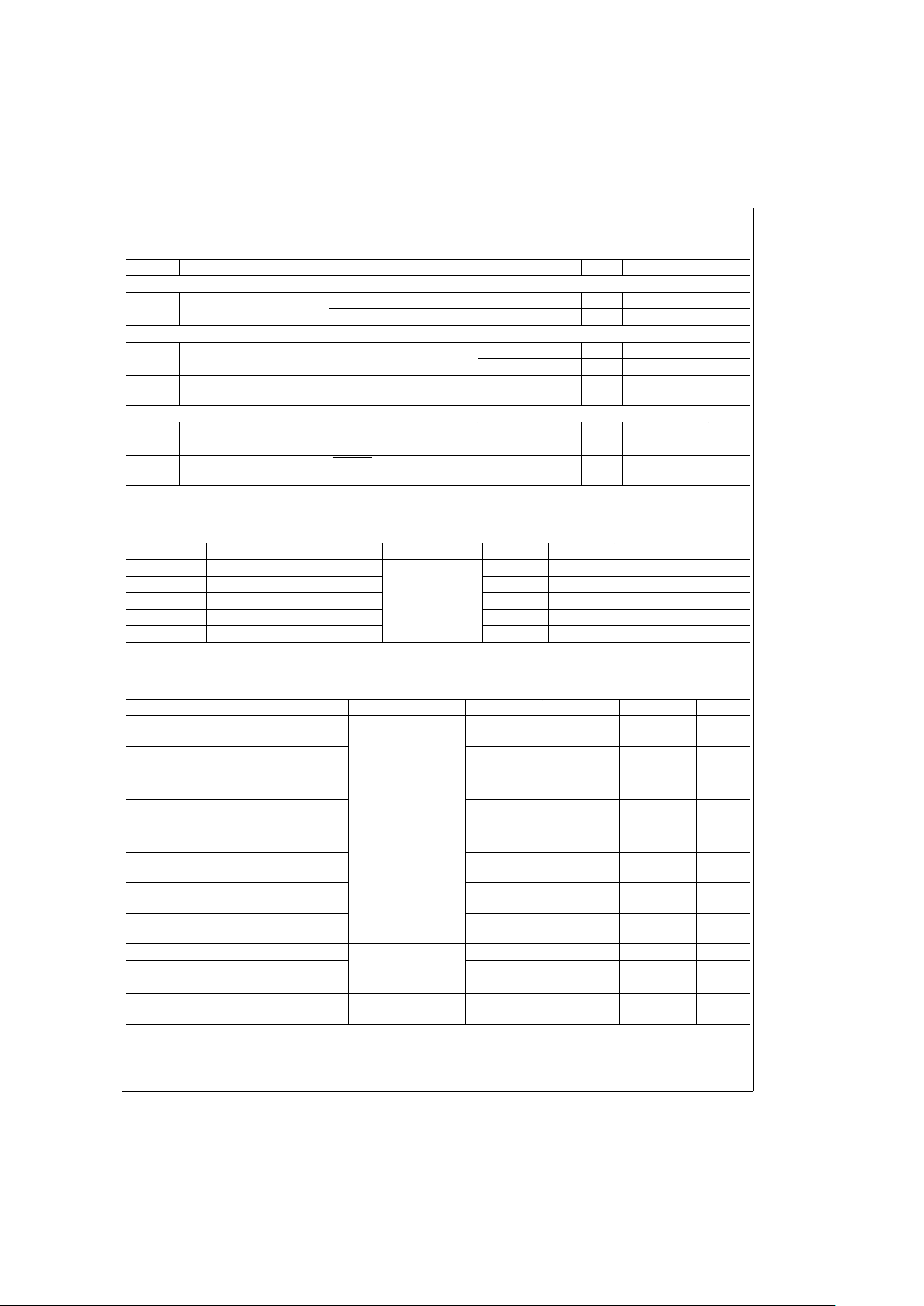
Electrical Characteristics
Over recommended operating supply and temperature ranges unless otherwise specified.
Symbol Parameter Conditions Min Typ Max Units
SERIALIZER CMOS/TTL DC SPECIFICATIONS (apply to DIN0-9, TCLK, PWRDN, TCLK_R/F, SYNC1, SYNC2, DEN)
V
IH
High Level Input Voltage 2.0 V
CC
V
V
IL
Low Level Input Voltage GND 0.8 V
V
CL
Input Clamp Voltage ICL= −18 mA −1.5 V
I
IN
Input Current VIN= 0V or 3.6V −10
±
2 +10 µA
DESERIALIZER CMOS/TTL DC SPECIFICATIONS (apply to pins PWRDN, RCLK_R/ F, REN, REFCLK = inputs; apply to pins
ROUT, RCLK, LOCK = outputs)
V
IH
High Level Input Voltage 2.0 V
CC
V
V
IL
Low Level Input Voltage GND 0.8 V
V
CL
Input Clamp Voltage ICL= −18 mA −0.62 −1.5 V
I
IN
Input Current VIN= 0V or 3.6V −10
±
1 +10 µA
V
OH
High Level Output Voltage IOH= −9 mA 2.1 2.93 V
CC
V
V
OL
Low Level Output Voltage IOL= 9 mA GND 0.33 0.6 V
I
OS
Output Short Circuit Current VOUT = 0V −15 −38 −85 mA
I
OZ
TRI-STATE Output Current PWRDN or REN = 0.8V, V
OUT
=0VorVCC −10±0.4 +10 µA
SERIALIZER Bus LVDS DC SPECIFICATIONS (apply to pins DO+ and DO−)
V
OD
Output Differential Voltage
(DO+)–(DO−)
RL=27Ω
200 270 mV
∆V
OD
Output Differential Voltage
Unbalance
35 mV
V
OS
Offset Voltage 0.78 1.1 1.3 V
∆V
OS
Offset Voltage Unbalance 35 mV
I
OS
Output Short Circuit Current D0 = 0V, DIN = High,PWRDN and DEN = 2.4V −10 −15 mA
I
OZ
TRI-STATE Output Current PWRDN or DEN = 0.8V, DO = 0V or VCC −10
±
1 +10 µA
I
OX
Power-Off Output Current VCC = 0V, DO = 0V or VCC −20
±
1 +20 µA
DESERIALIZER Bus LVDS DC SPECIFICATIONS (apply to pins RI+ and RI−)
VTH Differential Threshold High
Voltage
VCM = +1.1V
+19 +100 mV
VTL Differential Threshold Low
Voltage
−100 −7 mV
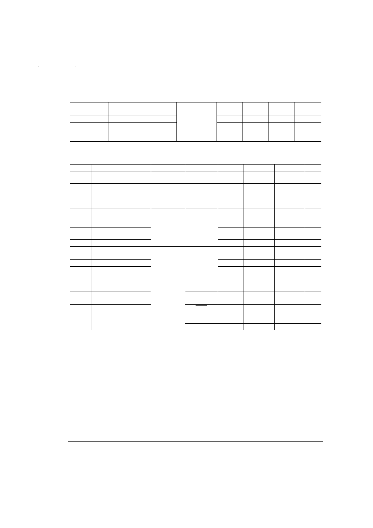
www.national.com 4
Page 5
Electrical Characteristics (Continued)
Over recommended operating supply and temperature ranges unless otherwise specified.
Symbol Parameter Conditions Min Typ Max Units
DESERIALIZER Bus LVDS DC SPECIFICATIONS (apply to pins RI+ and RI−)
I
IN
Input Current VIN= +2.4V, VCC= 3.6V or 0V −10
±
1 +10 µA
V
IN
= 0V, VCC= 3.6V or 0V −15
±
1 +15 µA
SERIALIZER SUPPLY CURRENT (apply to pins DVCC and AVCC)
I
CCD
Serializer Supply Current RL = 27Ω f = 40 MHz 32 55 mA
Worst Case
Figure 1
f = 16 MHz 25 45 mA
I
CCXD
Serializer Supply Current
Powerdown
PWRDN = 0.8V
410mA
DESERIALIZER SUPPLY CURRENT (apply to pins DVCC and AVCC)
I
CCR
Deserializer Supply Current CL= 15 pF f = 40 MHz 44 75 mA
Worst Case
Figure 2
f = 16 MHz 31 55 mA
I
CCXR
Deserializer Supply Current
Powerdown
PWRDN = 0.8V, REN = 0.8V
1.5 5.0 mA
Serializer Timing Requirements for TCLK
Over recommended operating supply and temperature ranges unless otherwise specified.
Symbol Parameter Conditions Min Typ Max Units
t
TCP
Transmit Clock Period 25 T 62.5 ns
t
TCIH
Transmit Clock High Time 0.4T 0.5T 0.6T ns
t
TCIL
Transmit Clock Low Time 0.4T 0.5T 0.6T ns
t
CLKT
TCLK Input Transition Time 3 6 ns
t
JIT
TCLK Input Jitter 150 ps
Serializer Switching Characteristics
Over recommended operating supply and temperature ranges unless otherwise specified.
Symbol Parameter Conditions Min Typ Max Units
t
LLHT
Bus LVDS Low-to-High
Transition Time
RL=27Ω
Figure 3
CL=10pF to GND
0.2 1 ns
t
LHLT
Bus LVDS High-to-Low
Transition Time
0.25 1 ns
t
DIS
DIN (0-9) Setup to TCLK
Figure 6
RL=27Ω,
C
L
=10pF to GND
1.0 0 ns
t
DIH
DIN (0-9) Hold from TCLK
6.5 4.5 ns
t
HZD
DO±HIGH to
TRI-STATE Delay
Figure 7
(Note 4)
R
L
=27Ω,
C
L
=10pF to GND
3.5 10 ns
t
LZD
DO±LOW to TRI-STATE
Delay
2.9 10 ns
t
ZHD
DO±TRI-STATE to HIGH
Delay
2.5 10 ns
t
ZLD
DO±TRI-STATE to LOW
Delay
2.7 10 ns
t
SPW
SYNC Pulse Width
Figure 8
RL=27Ω
1024*t
TCP
1029*t
TCP
ns
t
PLD
Serializer PLL Lock Time 2048*t
TCP
2049*t
TCP
ns
t
SD
Serializer Delay
Figure 9
RL=27Ω t
TCP
t
TCP
+ 2.5 t
TCP
+5 ns
t
BIT
Bus LVDS Bit Width RL=27Ω,
C
L
=10pF to GND
t
CLK
/12 ns
www.national.com5
Page 6
Deserializer Timing Requirements for REFCLK
Over recommended operating supply and temperature ranges unless otherwise specified.
Symbol Parameter Conditions Min Typ Max Units
t
RFCP
REFCLK Period 25 T 62.5 ns
t
RFDC
REFCLK Duty Cycle 50
%
t
RFCP/tTCP
Ratio of REFCLK to TCLK
Periods
0.83 1 1.03
t
RFTT
REFCLK Transition Time 3 6 ns
Deserializer Switching Characteristics
Over recommended operating supply and temperature ranges unless otherwise specified.
Symbol Parameter Conditions Pin/Freq. Min Typ Max Units
t
RCP
Receiver out Clock
Period
Figure 9
t
RCP=tTCP
RCLK
25 62.5 ns
t
CLH
CMOS/TTL Low-to-High
Transition Time
CL=15pF
Figure 4
Rout(0-9),
25ns
t
CHL
CMOS/TTL High-to-Low
Transition Time
LOCK, RCLK
25ns
t
DD
Deserializer Delay
Figure 10
1.75*t
RCP
1.75*t
RCP
+3 1.75*t
RCP
+7 ns
t
ROS
ROUT (0-9) Setup Data to
RCLK
Figure 11
RCLK
0.4*t
RCP
0.5*t
RCP
ns
t
ROH
ROUT (0-9) Hold Data to
RCLK
−0.4*t
RCP
−0.5*t
RCP
ns
t
RDC
RCLK Duty Cycle 40 50 60
%
t
HZR
HIGH to TRI-STATE Delay
Figure 12
Rout(0-9),
LOCK
4+0.5*t
RCP
10+t
RCP
ns
t
LZR
LOW to TRI-STATE Delay 4.2+0.5*t
RCP
10+t
RCP
ns
t
ZHR
TRI-STATE to HIGH Delay 6+0.5*t
RCP
12+t
RCP
ns
t
ZLR
TRI-STATE to LOW Delay 6.5+0.5*t
RCP
12+t
RCP
ns
t
DSR1
Deserializer PLL Lock Time
from PWRDWN (with
SYNCPAT)
(Note 5)
Figure 13
Figure 14
16MHz
715µs
40MHz
4.8 25.6 µs
t
DSR2
Deserializer PLL Lock time
from SYNCPAT
16MHz 7 10 µs
40MHz 4.5 7 µs
t
ZHLK
TRI-STATE to HIGH Delay
(power-up)
LOCK
1.5 12 ns
t
RNM
Deserializer Noise Margin
Figure 15
(Note 6)
16 MHz 400 1100 ps
40 MHz 100 400 ps
Note 1: “Absolute Maximum Ratings” are those values beyond which the safety of the device cannot be guaranteed. They are not meant to imply that the devices
should be operated at these limits. The table of “Electrical Characteristics” specifies conditions of device operation.
Note 2: Typical values are given for V
CC
= 3.3V and TA= +25˚C.
Note 3: Current into device pins is defined as positive. Current out of device pins is defined as negative. Voltages are referenced to ground except VOD, ∆VOD, VTH
and VTL which are differential voltages.
Note 4: Due to TRI-STATE of the Serializer, the Deserializer will lose PLL lock and have to resynchronize before data transfer.
Note 5: For the purpose of specifying deserializer PLL performance tDSR1 and tDSR2 are specified with the REFCLK running and stable, and specific conditions
of the incoming data stream (SYNCPATs). It is recommended that the derserializer be initialized using either tDSR1 timing or tDSR2 timing. tDSR1 is the time required
for the deserializer to indicate lock upon power-up or when leaving the power-down mode. Synchronization patterns should be sent to the device before initiating either condition. tDSR2 is the time required to indicate lock for the powered-up and enabled deserializer when the input (RI+ and RI-) conditions change from not receiving data to receiving synchronization patterns (SYNCPATs).
Note 6: tRNM is a measure of how much phase noise (jitter) the deserializer can tolerate in the incoming data stream before bit errors occur.
www.national.com 6
Page 7

AC Timing Diagrams and Test Circuits
DS100110-3
FIGURE 1. “Worst Case” Serializer ICC Test Pattern
DS100110-4
FIGURE 2. “Worst Case” Deserializer ICC Test Pattern
DS100110-5
FIGURE 3. Serializer Bus LVDS Output Load and Transition Times
DS100110-6
FIGURE 4. Deserializer CMOS/TTL Output Load and Transition Times
DS100110-7
FIGURE 5. Serializer Input Clock Transition Time
www.national.com7
Page 8

AC Timing Diagrams and Test Circuits (Continued)
DS100110-8
Timing shown for TCLK_R/F = LOW
FIGURE 6. Serializer Setup/Hold Times
DS100110-9
FIGURE 7. Serializer TRI-STATE Test Circuit and Timing
DS100110-10
FIGURE 8. Serializer PLL Lock Time, SYNC Timing and PWRDN TRI-STATE Delays
www.national.com 8
Page 9

AC Timing Diagrams and Test Circuits (Continued)
DS100110-11
FIGURE 9. Serializer Delay
DS100110-12
FIGURE 10. Deserializer Delay
DS100110-13
Timing shown for RCLK_R/F = LOW
Duty Cycle (t
RDC
)=
FIGURE 11. Deserializer Setup and Hold Times
www.national.com9
Page 10

AC Timing Diagrams and Test Circuits (Continued)
DS100110-14
FIGURE 12. Deserializer TRI-STATE Test Circuit and Timing
DS100110-15
FIGURE 13. Deserializer PLL Lock Times and PWRDN TRI-STATE Delays
www.national.com 10
Page 11

AC Timing Diagrams and Test Circuits (Continued)
DS100110-22
FIGURE 14. Deserializer PLL Lock Time from SyncPAT
DS100110-21
SW - Setup and Hold Time (Internal data sampling window)
t
JIT
- Serializer Output Bit Position Jitter
t
RSM
= Receiver Sampling Margin Time
FIGURE 15. Receiver Bus LVDS Input Skew Margin
DS100110-16
V
OD
=
(DO
+
)–(DO−).
Differential output signal is shown as (DO+)–(DO−), device in Data Transfer mode.
www.national.com11
Page 12

Application Information
Using the DS92LV1021 and DS92LV1210
The Serializer and Deserializer chipset is an easy to use
transmitter and receiver pair that sends 10 bits of parallel
TTL data over a serial Bus LVDS link up to 400 Mbps. Serialization of the input data is accomplished using an onboard
PLL at the Serializer which embeds two clock bits with the
data. The Deserializer uses a separate reference clock
(REFCLK) and an onboard PLL to extract the clock information from the incoming data stream and deserialize the data.
The Deserializer monitors the incoming clock information to
determine lock status and will indicate loss of lock by raising
the LOCK output.
Power Considerations
All CMOS design of the Serializer and Deserializer makes
them inherently low power devices. Additionally, the constant
current source nature of the Bus LVDSoutputs minimize the
slope of the speed vs. I
CC
curve of CMOS designs.
Powering Up the Serializer
The DS92LV1021 must be powered up using a specific sequence to properly start the PLL up. Not following the sequence can cause the Bus LVDS outputs to be stuck in a
certain output state. This may occur if the TCLK input is
driven before power is applied to the Serializer. It is important to note that this is not a latch up condition: no excessive
current is drawn by the Serializer in this state and the power
does not need to be cycled to recover from this state. Cycling
the PWRDWN pin from high to low and back to high will reset
the PLL and return the Serializer to normal operation.
To avoid this condition, the Serializer should be powered up
(ALL V
CC
pins) simultaneously with the PWRDWN pin held
low for 1µs. Once the V
CC
pins have stabilized the TCLK input can be driven and the Serializer will be ready for data
transmission.
Powering Up the Deserializer
The DS92LV1210 can be powered up at any time following
the proper sequence. The REFCLK input can be running before the Deserializer is powered up and it must be running in
order for the Deserializer to lock to incoming data. The Deserializer outputs will remain in TRI-STATE
™
until the Deserializer detects data transmission at its inputs and locks to the
incoming stream. The recommended power up sequence for
the deserializer is to power up all V
CC
pins simultaneously
with the PWRDWN pin held low for 1µs. Once the V
CC
pins
have stabilized the Deserializer is ready for locking. Another
option to ensure proper power up is to cycle the PWRDWN
pin from high to low and back to high after power up.
Transmitting Data
Once the Serializer and Deserializer are powered up and
running they must be phase locked to each other in order to
transmit data. Phase locking is accomplished by the Serializer sending SYNC patterns to the Deserializer. SYNC patterns are sent by the Serializer whenever SYNC1 or SYNC2
inputs are held high. The LOCK output of the Deserializer is
high whenever the Deserializer is not locked. Connecting the
LOCK output of the Deserializer to one of the SYNC inputs of
the Serializer will guarantee that enough SYNC patterns are
sent to achieve Deserializer lock.
While the Deserializer LOCK output is low,data at the Deserializer outputs (ROUT0-9) is valid except for the specific
case of loss of lock during transmission.
www.national.com 12
Page 13

Application Information (Continued)
Noise Margin
The Deserializer noise margin is the amount of input jitter
(phase noise) that the Deserializer can tolerate and still reliably receive data. Variousenvironmental and systematic factors include:
Serializer: TCLK jitter, V
CC
noise (noise bandwidth and
out-of-band noise)
Media: ISI, V
CM
noise
Deserializer: V
CC
noise
Recovering from LOCK Loss
In the case where the Serializer loses lock during data transmission up to 5 cycles of data that was previously received
can be invalid. This is due to the delay in the lock detection
circuit. The lock detect circuit requires that invalid clock information be received 4 times in a row to indicate loss of lock.
Since clock information has been lost it is possible that data
was also lost during these cycles. When the Deserializer
LOCK pin goes low, data from at least the previous 5 cycles
should be resent upon regaining lock.
Lock can be regained at the Deserializer by causing the Serializer to resend SYNC patterns as described above.
PCB Considerations
The Bus LVDS devices Serializer and Deserializer should be
placed as close to the edge connector as possible. In multiple Deserializer applications, the distance from the Deseri-
alizer to the slot connector appears as a stub to the Serializer driving the backplane traces. Longer stubs lower the
impedance of the bus increasing the load on the Serializer
and lowers threshold margin at the Deserializers. Deserializer devices should be placed no more than 1 inch from the
slot connector.
Transmission Media
The Serializer and Deserializer are designed for data transmission over a multi-drop bus. Multi-drop buses use a single
Serializer and multiple Deserializer devices. Since the Serializer can be driving from any point on the bus, the bus must
be terminated at both ends. For example, a 100 Ohm differential bus must be terminated at each end with 100 Ohms
lowering the DC impedance that the Serializer must drive to
50 Ohms. This load is further lowered by the addition of multiple Deserializers. Adding up to 20 Deserializers to the bus
(depending upon spacing) will lower the total load to about
27 Ohms (54 Ohm bus). The Serializer is designed for DC
loads between 27 and 100 Ohms.
The Serializer and Deserializer can also be used in
point-to-point configuration of a backplane, PCB trace or
through a twisted pair cable. In point-to-point configurations
the transmission media need only be terminated at the receiver end. In the point-to-point configuration the potential of
offsetting the ground levels of the Serializer vs. the Deserializer must be considered. Bus LVDS provides a plus / minus
one volt common mode range at the receiver inputs.
www.national.com13
Page 14

Pin Diagrams
DS92LV1021TMSA - Serializer
DS100110-18
DS92LV1210TMSA - Deserializer
DS100110-19
www.national.com 14
Page 15

Serializer Pin Description
Pin Name I/O No. Description
DIN I 3–12 Data Input. TTL levels inputs. Data on these pins are loaded into
a 10-bit input register.
TCLK_R/F
I 13 Transmit Clock Rising/Falling strobe select. TTL level input.
Selects TCLK active edge for strobing of DIN data. High selects
rising edge. Low selects falling edge.
DO+ O 22 + Serial Data Output. Non-inverting Bus LVDS differential output.
DO− O 21 − Serial Data Output. Inverting Bus LVDS differential output.
DEN I 19 Serial Data Output Enable. TTL level input. A low, puts the Bus
LVDS outputs in TRI-STATE.
PWRDN
I 24 Powerdown. TTL level input. PWRDN driven low shuts down the
PLL and TRI-STATEs outputs putting the device into a low power
sleep mode.
TCLK I 14 Transmit Clock. TTL level input. Input for 16 MHz–40 MHz
(nominal) system clock.
SYNC I 1, 2 Assertion of SYNC (high) for at least 1024 synchronization
symbols to be transmitted on the Bus LVDS serial output.
Synchronization symbols continue to be sent if SYNC continues
asserted. TTL level input. The two SYNC pins are ORed.
DVCC I 27, 28 Digital Circuit power supply.
DGND I 15, 16 Digital Circuit ground.
AVCC I 17, 26 Analog power supply (PLL and Analog Circuits).
AGND I 18, 25, 20, 23 Analog ground (PLL and Analog Circuits).
www.national.com15
Page 16

Deserializer Pin Description
Pin Name I/O No. Description
ROUT O 15–19,
24–28
Data Output.
±
9 mA CMOS level outputs.
RCLK_R/F
I 2 Recovered Clock Rising/Falling strobe select. TTL level input.
Selects RCLK active edge for strobing of ROUT data. High
selects rising edge. Low selects falling edge.
RI+ I 5 + Serial Data Input. Non-inverting Bus LVDS differential input.
RI− I 6 − Serial Data Input. Inverting Bus LVDS differential input.
PWRDN
I 7 Powerdown. TTL level input. PWRDN driven low shuts down the
PLL and TRI-STATEs outputs putting the device into a low power
sleep mode.
LOCK
O 10 LOCK goes low when the Deserializer PLL locks onto the
embedded clock edge. CMOS level output. Totem pole output
structure, does not directly support wire OR connection.
RCLK O 9 Recovered Clock. Parallel data rate clock recovered from
embedded clock. Used to strobe ROUT, CMOS level output.
REN I 8 Output Enable. TTL level input. TRI-STATEs ROUT0–ROUT9,
LOCK and RCLK when driven low.
DVCC I 21, 23 Digital Circuit power supply.
DGND I 14, 20, 22 Digital Circuit ground.
AVCC I 4, 11 Analog power supply (PLL and Analog Circuits).
AGND I 1, 12, 13 Analog ground (PLL and Analog Circuits).
REFCLK I 3 Use this pin to supply a REFCLK signal for the internal PLL
frequency.
www.national.com 16
Page 17

Truth Table
DIN (0–9) TCLK_R/F TCLK SYNC1/SYNC2 DEN PWRDN DO+ DO−
XX X XX0ZZ
XX X X01ZZ
X X SYSTEM CLK 1
z
1 1 SYNC PTRN SYNC PTRN*
DATA 1
L
0 1 1 DATA (0–9) DATA (0–9)*
DATA 0
K
0 1 1 DATA (0–9) DATA (0–9)*
RI RI− RCLK_R/F
REFCLK REN PWRDN RCLK LOCK ROUT (0–9)
XXX XX0ZZZ
X X X X 0** 1 Z Z Z
SYNC PTRN SYNC PTRN* X SYSTEM CLK 1 1 CLK 1
†
SYNC PTRN
DATA (0–9) DATA (0–9)* 1 SYSTEM CLK 1 1
L
0 DATA
DATA (0–9) DATA (0–9)* 0 SYSTEM CLK 1 1
K
0 DATA
z
Pulse 5-bits
* Inverted
†
Must be 1 before SYNC PTRN starts
** Device must be locked first
www.national.com17
Page 18

Physical Dimensions inches (millimeters) unless otherwise noted
LIFE SUPPORT POLICY
NATIONAL’S PRODUCTS ARE NOT AUTHORIZED FOR USE AS CRITICAL COMPONENTS IN LIFE SUPPORT
DEVICES OR SYSTEMS WITHOUT THE EXPRESS WRITTEN APPROVAL OF THE PRESIDENT OF NATIONAL
SEMICONDUCTOR CORPORATION. As used herein:
1. Life support devices or systems are devices or
systems which, (a) are intended for surgical implant
into the body, or (b) support or sustain life, and
whose failure to perform when properly used in
accordance with instructions for use provided in the
labeling, can be reasonably expected to result in a
significant injury to the user.
2. A critical component is any component of a life
support device or system whose failure to perform
can be reasonably expected to cause the failure of
the life support device or system, or to affect its
safety or effectiveness.
National Semiconductor
Corporation
Americas
Tel: 1-800-272-9959
Fax: 1-800-737-7018
Email: support@nsc.com
National Semiconductor
Europe
Fax: +49 (0) 1 80-530 85 86
Email: europe.support@nsc.com
Deutsch Tel: +49 (0) 1 80-530 85 85
English Tel: +49 (0) 1 80-532 78 32
Français Tel: +49 (0) 1 80-532 93 58
Italiano Tel: +49 (0) 1 80-534 16 80
National Semiconductor
Asia Pacific Customer
Response Group
Tel: 65-2544466
Fax: 65-2504466
Email: sea.support@nsc.com
National Semiconductor
Japan Ltd.
Tel: 81-3-5639-7560
Fax: 81-3-5639-7507
www.national.com
Order Number DS92LV1021TMSA or DS92LV1210TMSA
NS Package Number MSA28
DS92LV1021/DS92LV1210 16-40 MHz 10 Bit Bus LVDS Serializer and Deserializer
National does not assume any responsibility for use of any circuitry described, no circuit patent licenses are implied and National reserves the right at any time without notice to change said circuitry and specifications.
 Loading...