

Page 1
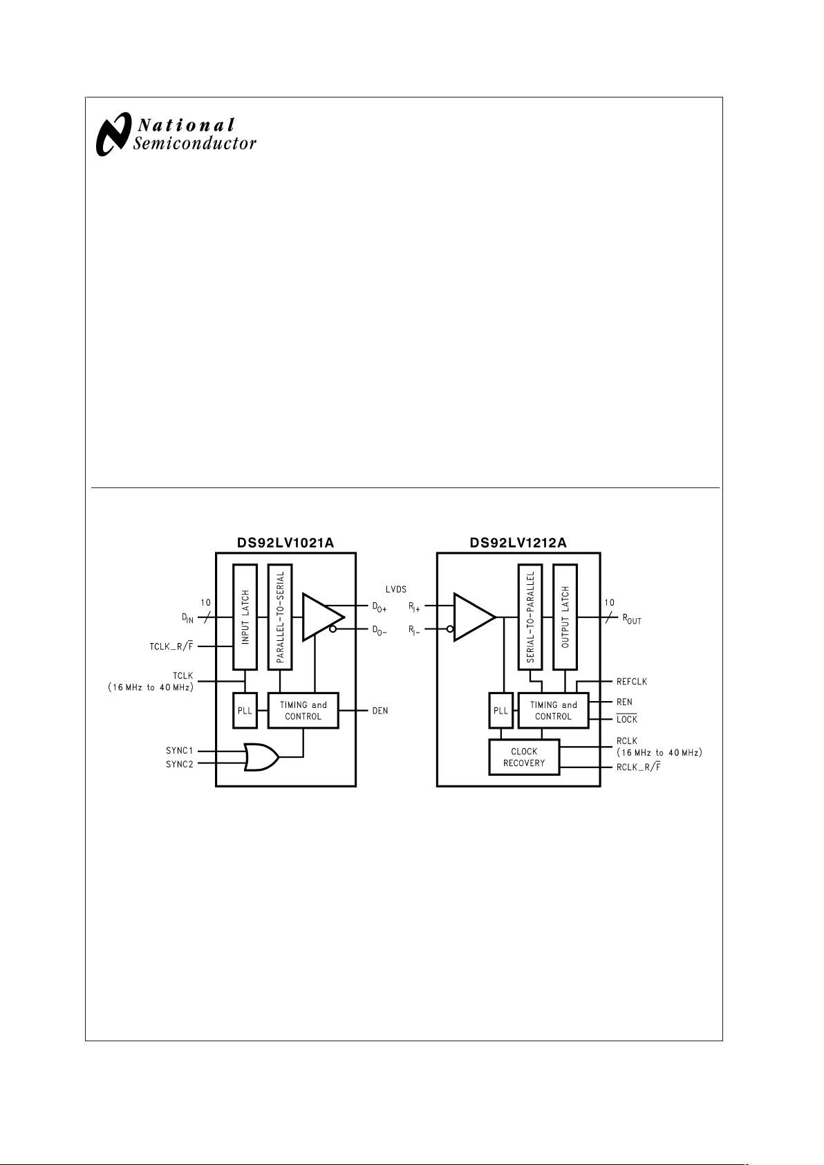
DS92LV1021A
16-40 MHz 10 Bit Bus LVDS Serializer
General Description
The DS92LV1021A transforms a 10-bit wide parallel
LVCMOS/LVTTL data bus into a single high speed Bus
LVDS serial data stream with embedded clock. The
DS92LV1021A can transmit data over backplanes or cable.
The single differential pair data path makes PCB design
easier. In addition, the reduced cable, PCB trace count, and
connector size tremendously reduce cost. Since one output
transmits both clock and data bits serially, it eliminates clockto-data and data-to-data skew. The powerdown pin saves
power by reducing supply current when the device is not
being used. Upon power up of the Serializer, you can choose
to activate synchronization mode or use one of National
Semiconductor’s Deserializers in the synchronization-torandom-data feature. By using the synchronization mode,
the Deserializer will establish lock to a signal within specified
lock times. In addition, the embedded clock guarantees a
transition on the bus every 12-bit cycle. This eliminates
transmission errors due to charged cable conditions. Furthermore, you may put the DS92LV1021A output pins into
TRI-STATE
®
to achieve a high impedance state. The PLL
can lock to frequencies between 16 MHz and 40 MHz.
Features
n Guaranteed transition every data transfer cycle
n Single differential pair eliminates multi-channel skew
n Flow-through pinout for easy PCB layout
n 400 Mbps serial Bus LVDS bandwidth (at 40 MHz clock)
n 10-bit parallel interface for 1 byte data plus 2 control bits
n Programmable edge trigger on clock
n Bus LVDS serial output rated for 27Ω load
n Small 28-lead SSOP package-MSA
Block Diagrams
20026901
TRI-STATE®is a registered trademark of National Semiconductor Corporation.
January 2003
DS92LV1021A 16-40 MHz 10 Bit Bus LVDS Serializer
© 2003 National Semiconductor Corporation DS200269 www.national.com
Page 2
Block Diagrams (Continued)
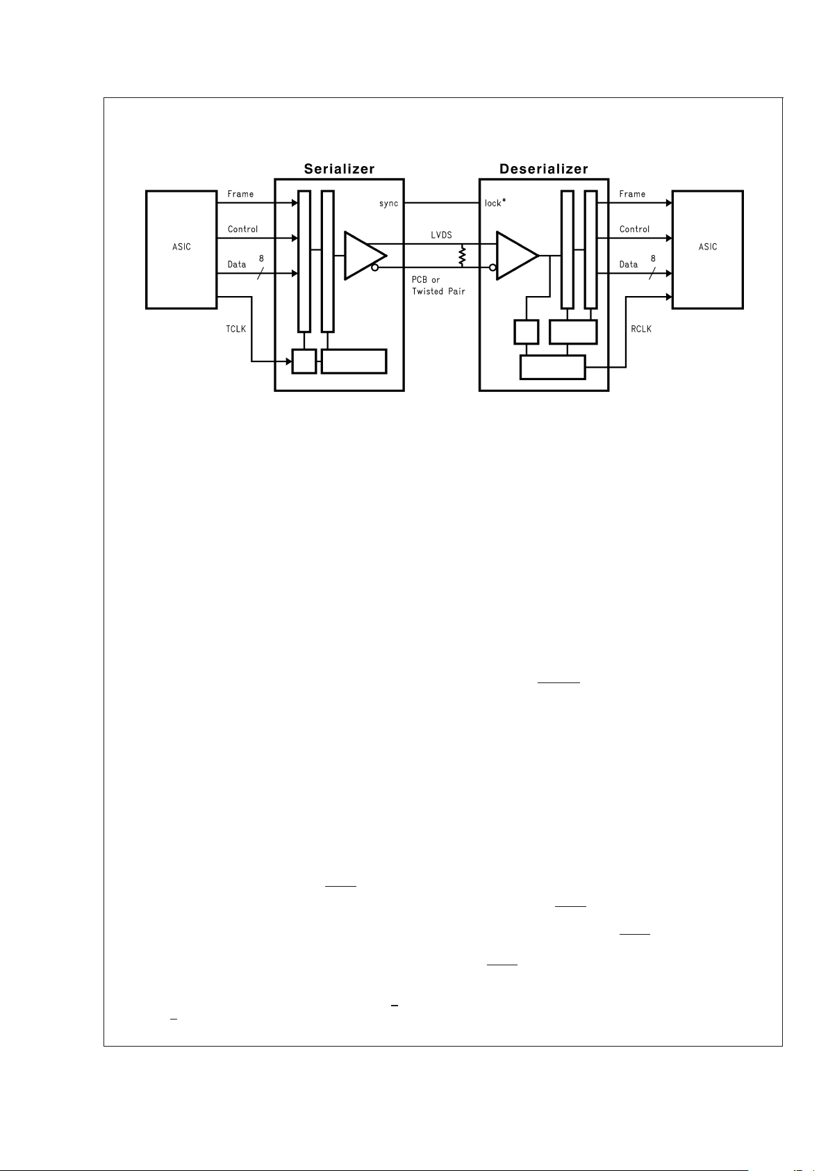
Application
20026902
Functional Description
The DS92LV1021A is an upgrade to the DS92LV1021. The
DS92LV1021A no longer has a power-up sequence requirement. Like the DS92LV1021, the DS92LV1021A is a 10-bit
Serializer designed to transmit data over a differential backplane at clock speeds from 16 to 40MHz. It may also be used
to drive data over Unshielded Twisted Pair (UTP) cable.
The DS92LV1021A can be used with any of National’s 10-bit
BLVDS Deserializers (DS92LV1212A for example) and has
three active states of operation: Initialization, Data Transfer,
and Resynchronization; and two passive states: Powerdown
and TRI-STATE.
The following sections describe each active and passive
state.
Initialization
Before data can be transferred, the Serializer must be initialized. Initialization refers to synchronization of the Serializer’s
PLL to a local clock.
When V
CC
is applied to the Serializer, the outputs are held in
TRI-STATE and internal circuitry is disabled by on-chip
power-on circuitry. When V
CC
reaches VCCOK (2.5V) the
Serializer’s PLL begins locking to the local clock. The local
clock is the transmit clock, TCLK, provided by the source
ASIC or other device.
Once the PLL locks to the local clock, the Serializer is ready
to send data or SYNC patterns, depending on the levels of
the SYNC1 and SYNC2 inputs. The SYNC pattern is composed of six ones and six zeros switching at the input clock
rate.
Control of the SYNC pins is left to the user. One recommendation is a direct feedback loop from the LOCK pin. Under all
circumstances, the Serializer stops sending SYNC patterns
after both SYNC inputs return low.
Data Transfer
After initialization, the Serializer inputs DIN0–DIN9 may be
used to input data to the Serializer. Data is clocked into the
Serializer by the TCLK input. The edge of TCLK used to
strobe the data is selectable via the TCLK_R/F pin.
TCLK_R/F high selects the rising edge for clocking data and
low selects the falling edge. If either of the SYNC inputs is
high for 5*TCLK cycles, the data at DIN0-DIN9 is ignored
regardless of the clock edge.
A start bit and a stop bit, appended internally, frame the data
bits in the register. The start bit is always high and the stop
bit is always low. The start and stop bits function as the
embedded clock bits in the serial stream.
Serialized data and clock bits (10+2 bits) are transmitted
from the serial data output (DO
±
) at 12 times the TCLK
frequency. For example, if TCLK is 40 MHz, the serial rate is
40 x 12 = 480 Mega bits per second. Since only 10 bits are
from input data, the serial “payload” rate is ten times the
TCLK frequency. For instance, if TCLK = 40 MHz, the payload data rate is 40 x 10 = 400 Mbps. TCLK is provided by
the data source and must be in the range of 16 MHz to 40
MHz nominal.
The outputs (DO
±
) can drive a backplane or a point-to-point
connection. The outputs transmit data when the enable pin
(DEN) is high, PWRDN is high, and SYNC1 and SYNC2 are
low. The DEN pin may be used to TRI-STATE the outputs
when driven low.
Ideal Crossing Point
The ideal crossing point is the best case start and stop point
for a normalized bit. Each ideal crossing point is found by
dividing the clock period by twelve--two clock bits plus ten
data bits. For example, a 40 MHz clock has a period of 25ns.
The 25ns divided by 12 bits is approximately 2.08ns. This
means that each bit width is approximately 2.08ns, and the
ideal crossing points occur every 2.08ns. For a graphical
representation, please see Figure 9.
Resynchronization
The Deserializer LOCK pin driven low indicates that the
Deserializer PLL is locked to the embedded clock edge. If
the Deserializer loses lock, the LOCK output will go high and
the outputs (including RCLK) will be TRI-STATE.
The LOCK pin must be monitored by the system to detect a
loss of synchronization, and the system must decide if it is
necessary to pulse the Serializer SYNC1 or SYNC2 pin to
resynchronize. There are multiple approaches possible. One
recommendation is to provide a feedback loop using the
DS92LV1021A
www.national.com 2
Page 3
Resynchronization (Continued)
LOCK pin itself to control the sync request of the Serializer
(SYNC1 or SYNC2).At the time of publication, other than the
DS92LV1210, all other Deserializers from National Semiconductor have random lock capability. This feature does not
require the system user to send SYNC patterns upon loss of
lock. However, lock times can only be guaranteed with transmission of SYNC patterns. Dual SYNC pins are provided for
multiple control in a multi-drop application.
Powerdown
The Powerdown state is a low power sleep mode that the
Serializer and Deserializer may use to reduce power when
no data is being transferred. The device enters Powerdown
when the PWRDN pin is driven low on the Serializer. In
Powerdown, the PLL stops and the outputs go into TRISTATE, disabling load current and reducing supply current
into the milliamp range. To exit Powerdown, PWRDN must
be driven high.
Both the Serializer and Deserializer must reinitialize and
resynchronize before data can be transferred. The Deserializer will initialize and assert LOCK high until it is locked to the
Bus LVDS clock.
TRI-STATE
For the Serializer, TRI-STATE is entered when the DEN pin
is driven low. This will TRI-STATE both driver output pins
(DO+ and DO−). When DEN is driven high, the serializer will
return to the previous state as long as all other control pins
remain static (SYNC1, SYNC2, PWRDN, TCLK_R/F).
Ordering Information
Order Number NSID Function Package
DS92LV1021AMSA Serializer MSA28
DS92LV1021A
www.national.com3
Page 4
Absolute Maximum Ratings (Note 1)
If Military/Aerospace specified devices are required,
please contact the National Semiconductor Sales Office/
Distributors for availability and specifications.
Supply Voltage (V
CC
) −0.3V to +4V
CMOS/TTL Input Voltage −0.3V to (V
CC
+0.3V)
CMOS/TTL Output
Voltage −0.3V to (V
CC
+0.3V)
Bus LVDS Receiver Input
Voltage −0.3V to +3.9V
Bus LVDS Driver Output
Voltage −0.3V to +3.9V
Bus LVDS Output Short
Circuit Duration Continuous
Junction Temperature +150˚C
Storage Temperature −65˚C to +150˚C
Lead Temperature
(Soldering, 4 seconds) +260˚C
Maximum Package Power Dissipation Capacity
@
25˚C Package:
28L SSOP 1.27 W
Package Derating:
28L SSOP
10.2 mW/˚C above
+25˚C
ESD Rating (HBM)
>
2.0kV
(Note 1)
Note 1: With a limited Engineering sample size,
ESD (HBM) testing passed 2.5kV
Recommended Operating
Conditions
Min Nom Max Units
Supply Voltage (V
CC
) 3.0 3.3 3.6 V
Operating Free Air
Temperature (TA)
−40 +25 +85 ˚C
Supply Noise Voltage
(V
CC
)
100 mV
P-P
Electrical Characteristics
Over recommended operating supply and temperature ranges unless otherwise specified.
Symbol Parameter Conditions Min Typ Max Units
SERIALIZER CMOS/TTL DC SPECIFICATIONS (apply to DIN0-9, TCLK, PWRDN, TCLK_R/F, SYNC1, SYNC2, DEN)
V
IH
High Level Input Voltage 2.0 V
CC
V
V
IL
Low Level Input Voltage GND 0.8 V
V
CL
Input Clamp Voltage ICL= −18 mA −1.5 V
I
IN
Input Current VIN= 0V or 3.6V −10
±
2 +10 µA
SERIALIZER Bus LVDS DC SPECIFICATIONS (apply to pins DO+ and DO−)
V
OD
Output Differential Voltage
(DO+)–(DO−)
RL=27Ω
200 270 mV
∆V
OD
Output Differential Voltage
Unbalance
35 mV
V
OS
Offset Voltage 0.78 1.1 1.3 V
∆V
OS
Offset Voltage Unbalance 35 mV
I
OS
Output Short Circuit Current D0 = 0V, DIN = High,PWRDN and DEN = 2.4V −30 −40 mA
I
OZ
TRI-STATE Output Current PWRDN or DEN = 0.8V, DO = 0V or VCC −10
±
1 +10 µA
I
OX
Power-Off Output Current VCC = 0V, DO = 0V or VCC −20
±
1 +20 µA
SERIALIZER SUPPLY CURRENT (apply to pins DVCC and AVCC)
I
CCD
Worst Case Serializer Supply
Current
RL=27Ω,
Figure 1
f = 40 MHz 40 55 mA
f = 16 MHz 28 35 mA
I
CCXD
Serializer Supply Current
Powerdown
PWRDN = 0.8V
88 300 µA
DS92LV1021A
www.national.com 4
Page 5

Serializer Timing Requirements for TCLK
Over recommended operating supply and temperature ranges unless otherwise specified.
Symbol Parameter Conditions Min Typ Max Units
t
TCP
Transmit Clock Period 25 T 62.5 ns
t
TCIH
Transmit Clock High Time 0.4T 0.5T 0.6T ns
t
TCIL
Transmit Clock Low Time 0.4T 0.5T 0.6T ns
t
CLKT
TCLK Input Transition
Time
36ns
t
JIT
TCLK Input Jitter
150
ps
(RMS)
Serializer Switching Characteristics
Over recommended operating supply and temperature ranges unless otherwise specified.
Symbol Parameter Conditions Min Typ Max Units
t
LLHT
Bus LVDS
Low-to-High
Transition Time
R
L
=27Ω,
Figure 2,
C
L
=10pF to GND
0.31 0.75 ns
t
LHLT
Bus LVDS
High-to-Low
Transition Time
0.30 0.75 ns
t
DIS
DIN (0-9) Setup to
TCLK
Figure 4,
R
L
=27Ω,
C
L
=10pF to GND
0ns
t
DIH
DIN (0-9) Hold from
TCLK
4.0 ns
t
HZD
DO±HIGH to
TRI-STATE Delay
Figure 5 ,(Note 4),
R
L
=27Ω,
C
L
=10pF to GND
3.5 10 ns
t
LZD
DO±LOW to
TRI-STATE Delay
2.9 10 ns
t
ZHD
DO±TRI-STATE to
HIGH Delay
2.5 10 ns
t
ZLD
DO±TRI-STATE to
LOW Delay
2.7 10 ns
t
SPW
SYNC Pulse Width Figure 7,
R
L
=27Ω
5*t
TCP
ns
t
PLD
Serializer PLL Lock
Time
Figure 6,
R
L
=27Ω
510*t
TCP
2049*t
TCP
ns
t
SD
Serializer Delay Figure 8 ,RL=27Ω t
TCP
+1.0 t
TCP
+ 2.0 t
TCP
+4.0 ns
t
BIT
Bus LVDS Bit Width RL=27Ω,
C
L
=10pF to GND
t
CLK
/12 ns
t
DJIT
Deterministic Jitter
R
L
=27Ω,
C
L
=10pF to GND,
(Note 5)
f = 40 MHz −320 −110 150 ps
f = 16 MHz −800 −160 380 ps
Note 1: “Absolute Maximum Ratings” are those values beyond which the safety of the device cannot be guaranteed. They are not meant to imply that the devices
should be operated at these limits. The table of “Electrical Characteristics” specifies conditions of device operation.
Note 2: Typical values are given for V
CC
= 3.3V and TA= +25˚C.
Note 3: Current into device pins is defined as positive. Current out of device pins is defined as negative. Voltages are referenced to ground except VOD, ∆VOD,
VTH and VTL which are differential voltages.
Note 4: Due to TRI-STATE of the Serializer, the Deserializer will lose PLL lock and have to resynchronize before data transfer.
Note 5: t
DJIT
specifications are Guranteed By Design (GBD) using statistical analysis.
DS92LV1021A
www.national.com5
Page 6

AC Timing Diagrams and Test Circuits
20026903
FIGURE 1. “Worst Case” Serializer ICC Test Pattern
20026905
FIGURE 2. Serializer Bus LVDS Output Load and Transition Times
20026907
FIGURE 3. Serializer Input Clock Transition Time
20026908
Timing shown for TCLK_R/F = LOW
FIGURE 4. Serializer Setup/Hold Times
DS92LV1021A
www.national.com 6
Page 7

AC Timing Diagrams and Test Circuits (Continued)
20026909
FIGURE 5. Serializer TRI-STATE Test Circuit and Timing
20026925
FIGURE 6. Serializer PLL Lock Time, and PWRDN TRI-STATE Delays
DS92LV1021A
www.national.com7
Page 8

AC Timing Diagrams and Test Circuits (Continued)
20026926
FIGURE 7. SYNC Timing Delays
20026911
FIGURE 8. Serializer Delay
DS92LV1021A
www.national.com 8
Page 9

AC Timing Diagrams and Test Circuits (Continued)
Application Information
DIFFERENCES BETWEEN THE DS92LV1021A AND THE
DS92LV1021
The DS92LV1021A is an enhanced version of the
DS92LV1021. The following enhancements are provided by
the DS92LV1021A:
•
TCLK may be applied before power
•
TCLK may be halted
•
Slower typical edge rates help to reduce reflections
•
PWRDN pin includes an internal weak pull down device
Like the DS92LV1021, the DS92LV1021A is a 10-bit Serializer designed to transmit data over a differential backplane
at clock speeds from 16 to 40MHz. It may also be used to
drive data over Unshielded Twisted Pair (UTP) cable.
USING THE DS92LV1021A
The Serializer is an easy to use transmitter that sends 10 bits
of parallel TTL data over a serial Bus LVDS link up to 400
Mbps. Serialization of the input data is accomplished using
an onboard PLL which embeds two clock bits with the data.
POWER CONSIDERATIONS
An all CMOS design of the Serializer makes it an inherently
low power device. Additionally, the constant current source
nature of the Bus LVDS outputs minimize the slope of the
speed vs. I
CC
curve of CMOS designs.
DIGITAL AND ANALOG POWER PINS
Digital and Analog power supply pins should be at the same
voltage levels. The user should verify that voltage levels at
the digital and analog supply pins are at the same voltage
levels after board layout and after bypass capacitors are
added.
HOT INSERTION
All Bus LVDS devices are hot pluggable if you follow a few
rules. When inserting, ensure the Ground pin(s) makes contact first, then the VCC pin(s), and then the I/O pins. When
removing, the I/O pins should be unplugged first, then the
VCC, then the Ground.
TRANSMITTING DATA
Once the Serializer and Deserializer are powered up and
running they must be phase locked to each other in order to
transmit data. Phase locking can be accomplished by the
Serializer sending SYNC patterns to the Deserializer, or by
using the Deserializer’s random lock capability. SYNC patterns are sent by the Serializer whenever SYNC1 or SYNC2
inputs are held high. The LOCK output of the Deserializer is
high whenever the Deserializer is not locked. Connecting the
LOCK output of the Deserializer to one of the SYNC inputs of
the Serializer will guarantee that enough SYNC patterns are
sent to achieve Deserializer lock.
While the Deserializer LOCK output is low, data at the Deserializer outputs (ROUT0-9) is valid except for the specific
case of loss of lock during transmission.
RECOVERING FROM LOCK LOSS
In the case where the Serializer loses lock during data
transmission up to three cycles of data that was previously
received can be invalid. This is due to the delay in the lock
detection circuit. The lock detect circuit requires that invalid
clock information be received 4 times in a row to indicate
loss of lock. Since clock information has been lost it is
possible that data was also lost during these cycles. When
the Deserializer LOCK pin goes low, data from at least the
previous three cycles should be resent upon regaining lock.
Lock can be regained at the Deserializer by causing the
Serializer to resend SYNC patterns as described above.
20026923
For an explanation of the Ideal Crossing Point, please see the Application Information Section.
FIGURE 9. Serializer Deterministic Jitter and Ideal Crossing Point
DS92LV1021A
www.national.com9
Page 10

Application Information (Continued)
PCB CONSIDERATIONS
The Bus LVDS devices Serializer and Deserializer should be
placed as close to the edge connector as possible. In multiple Deserializer applications, the distance from the Deserializer to the slot connector appears as a stub to the Serializer driving the backplane traces. Longer stubs lower the
impedance of the bus increasing the load on the Serializer
and lowers threshold margin at the Deserializers. Deserializer devices should be placed no more than 1 inch from the
slot connector.
TRANSMISSION MEDIA
The Serializer and Deserializer are designed for data transmission over a multi-drop bus. Multi-drop buses use a single
Serializer and multiple Deserializer devices. Since the Seri-
alizer can be driving from any point on the bus, the bus must
be terminated at both ends. For example, a 100 Ohm differential bus must be terminated at each end with 100 Ohms
lowering the DC impedance that the Serializer must drive to
50 Ohms. This load is further lowered by the addition of
multiple Deserializers. Adding up to 20 Deserializers to the
bus (depending upon spacing) will lower the total load to
about 27 Ohms (54 Ohm bus). The Serializer is designed for
DC loads between 27 and 100 Ohms.
The Serializer and Deserializer can also be used in point-topoint configuration of a backplane, PCB trace or through a
twisted pair cable. In point-to-point configurations the transmission media need only be terminated at the receiver end.
In the point-to-point configuration the potential of offsetting
the ground levels of the Serializer vs. the Deserializer must
be considered. Bus LVDS provides a plus / minus one volt
common mode range at the receiver inputs.
Pin Diagram
DS92LV1021AMSA - Serializer
20026918
DS92LV1021A
www.national.com 10
Page 11

Serializer Pin Description
Pin Name I/O No. Description
DIN I 3–12 Data Input. TTL levels inputs. Data on these pins are loaded into a
10-bit input register.
TCLK_R/F
I 13 Transmit Clock Rising/Falling strobe select. TTL level input. Selects
TCLK active edge for strobing of DIN data. High selects rising
edge. Low selects falling edge.
DO+ O 22 + Serial Data Output. Non-inverting Bus LVDS differential output.
DO− O 21 − Serial Data Output. Inverting Bus LVDS differential output.
DEN I 19 Serial Data Output Enable. TTL level input. A low, puts the Bus
LVDS outputs in TRI-STATE.
PWRDN
I 24 Powerdown. TTL level input. PWRDN driven low shuts down the
PLL and TRI-STATEs the outputs putting the device into a low
power sleep mode. This pin has an internal weak pull down.
TCLK I 14 Transmit Clock. TTL level input. Input for 16 MHz–40 MHz
(nominal) system clock.
SYNC I 1, 2 Assertion of SYNC (high) for at least 1024 synchronization symbols
to be transmitted on the Bus LVDS serial output. Synchronization
symbols continue to be sent if SYNC continues asserted. TTL level
input. The two SYNC pins are ORed.
DVCC I 27, 28 Digital Circuit power supply. DVCC voltage level should be identical
to the AVCC voltage level.
DGND I 15, 16 Digital Circuit ground. Ground potential should be the same as
AGND.
AVCC I 17, 26 Analog power supply (PLL and Analog Circuits). AVCC voltage
level should be identical to the DVCC voltage level.
AGND I 18, 25, 20, 23 Analog ground (PLL and Analog Circuits). Ground potential should
be the same as DGND.
Truth Table
DIN (0– 9) TCLK_R/F TCLK SYNC1/SYNC2 DEN PWRDN DO+ DO−
XXX XX0ZZ
XXX X01ZZ
X X SYSTEM CLK 1∼ 1 1 SYNC PTRN SYNC PTRN*
DATA 1
L
0 1 1 DATA (0–9) DATA (0– 9)*
DATA 0
K
0 1 1 DATA (0–9) DATA (0– 9)*
RI RI− RCLK_R/F
REFCLK REN PWRDN RCLK LOCK
XXX XX0ZZ
X X X X 0** 1 Z Z
SYNC PTRN SYNC PTRN* X SYSTEM CLK 1 1 CLK 1
†
DATA (0– 9) DATA (0–9)* 1 SYSTEM CLK 1 1
L
0
DATA (0– 9) DATA (0–9)* 0 SYSTEM CLK 1 1
K
0
∼ Pulse 5-bits
* Inverted
†
Must be 1 before SYNC PTRN starts
** Device must be locked first
DS92LV1021A
www.national.com11
Page 12

Physical Dimensions inches (millimeters)
unless otherwise noted
Order Number DS92LV1021AMSA
NS Package Number MSA28
LIFE SUPPORT POLICY
NATIONAL’S PRODUCTS ARE NOT AUTHORIZED FOR USE AS CRITICAL COMPONENTS IN LIFE SUPPORT
DEVICES OR SYSTEMS WITHOUT THE EXPRESS WRITTEN APPROVAL OF THE PRESIDENT AND GENERAL
COUNSEL OF NATIONAL SEMICONDUCTOR CORPORATION. As used herein:
1. Life support devices or systems are devices or
systems which, (a) are intended for surgical implant
into the body, or (b) support or sustain life, and
whose failure to perform when properly used in
accordance with instructions for use provided in the
labeling, can be reasonably expected to result in a
significant injury to the user.
2. A critical component is any component of a life
support device or system whose failure to perform
can be reasonably expected to cause the failure of
the life support device or system, or to affect its
safety or effectiveness.
National Semiconductor
Americas Customer
Support Center
Email: new.feedback@nsc.com
Tel: 1-800-272-9959
National Semiconductor
Europe Customer Support Center
Fax: +49 (0) 180-530 85 86
Email: europe.support@nsc.com
Deutsch Tel: +49 (0) 69 9508 6208
English Tel: +44 (0) 870 24 0 2171
Français Tel: +33 (0) 1 41 91 8790
National Semiconductor
Asia Pacific Customer
Support Center
Fax: 65-6250 4466
Email: ap.support@nsc.com
Tel: 65-6254 4466
National Semiconductor
Japan Customer Support Center
Fax: 81-3-5639-7507
Email: nsj.crc@jksmtp.nsc.com
Tel: 81-3-5639-7560
www.national.com
DS92LV1021A 16-40 MHz 10 Bit Bus LVDS Serializer
National does not assume any responsibility for use of any circuitry described, no circuit patent licenses are implied and National reserves the right at any time without notice to change said circuitry and specifications.
 Loading...