

Page 1

PRODUCT BRIEF
Y
Maxim/Dallas Semiconductor Confidential
PRODUCT PREVIEW
DS3181,2,3,4 Multi-Port ATM/Packet PHYs
For DS3/E3 with Built-In LIUs
FEATURES
• Quad (DS3184), triple (DS3183), dual (DS3182) or single (DS3181) with integrated LIU ATM / Packet PHYs for DS3 and E3
• Each port independently configurable
• Performs receive clock/data recovery and
transmit wave shaping
• Jitter attenuators can be placed either in the receive or transmit paths
• Interfaces to 75Ω coaxial cable at lengths up
to 380 meters or 1246 feet (DS3) or 440
meters or 1443 feet (E3)
• Uses 1:2 transformers on both Tx and Rx
• Requires minimal external components
• Universal PHYs map ATM cells and/or
HDLC packets into DS3 or E3 data streams
• UTOPIA 2 or 3 or POS-PHY 2 or 3 interface with 8, 16, or 32 bit bus width up to 66 MHz
• Ports independently configurable for cell or packet traffic in POS-PHY bus modes
• Direct, PLCP and clear-channel cell mapping
• Direct and clear-channel packet mapping
• On-chip DS3 (M23 or C-bit) and E3 (G.751
or G.832) framers
• Ports independently configurable for DS3, E3 or arbitrary framing protocol up to 52 Mbps
• Programmable (externally controlled or internally hardware based engine) subrate DS3/E3 circuitry
• Full featured DS3/E3/PLCP alarms
• Built-in HDLC controllers with 256 byte
FIFOs for DS3 PMDL, G.751 Sn bit or G.832
NR/GC bytes
www.maxim-ic.com/telecom
PRODUCT BRIEF
PRODUCT BRIEF
PRELIMINAR
• On-chip BERTs for PRBS and repetitive pattern generation, detection and analysis
• Large performance-monitoring counters for accumulation intervals up to 1 second
• Flexible overhead insertion/extraction ports for DS3, E3 and PLCP framers
• Loopback include line, diagnostic, framer payload and system interface
• Ports can be disabled to reduce power
• Integrates clock rate adapter to generate the
required 44.736 MHz for DS3, 34.368 MHz
for E3, and/or 52 MHz for arbitrary framing
protocol up to 52 Mbps
• 8/16-bit generic microprocessor interface
• Low power 3.3V operation (5V tolerant I/O)
• Small high-density Thermally Enhanced (TE)
Chip Scale BGA packaging
• Industrial temperature range: -40 to +85°C
• IEEE 1149.1 JTAG test port
Note: This Product Preview contains preliminary information and is subject to change without notice.
Some revisions of this device may incorporate deviations from published specifications known as errata.
Multiple revisions of any device may be simultaneously available through various sales channels. For
information about device errata, visit: http://dbserv.maxim-ic.com/errata.cfm
Rev 1.5 1 of 13 022304
.
Page 2
Maxim/Dallas Semiconductor Confidential
r
PRODUCT PREVIEW
DS3181,2,3,4 Multi-Port ATM/Packet PHYs
For DS3/E3 with Built-In LIUs
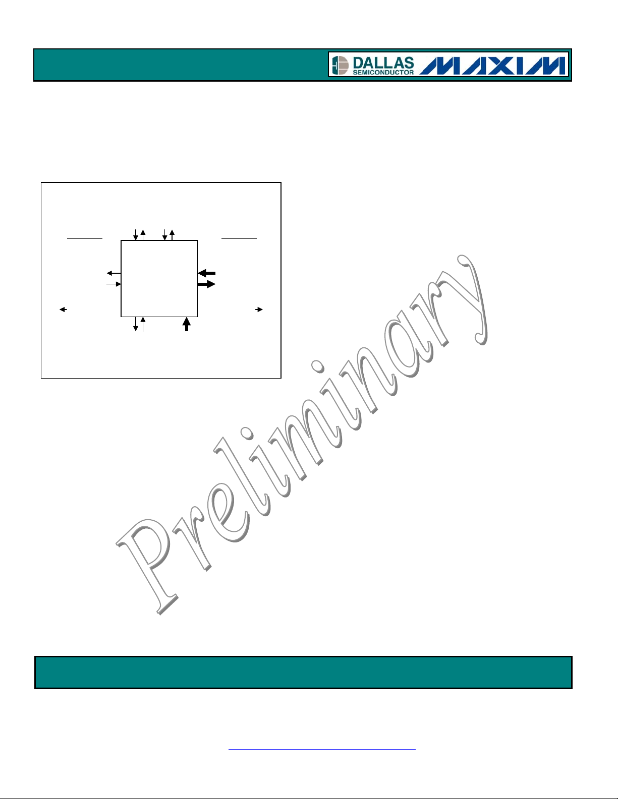
FUNCTIONAL DIAGRAM
Line
Interface
TXPn/TXNn
RXPn/RXNn
Ports[1:n]
To T3/E3
Transformers
DS3/E3
Overhead
Ports[1:n]
Frame
Interface
Ports[1:n]
PLCP
Overhead
Ports[1:n]
DS318x
Microprocessor
Interface
System
Interface
UTOPIA or
POS-PHY
bus
to ATM or
Link layer
ORDERING INFORMATION
Commercial Temperature Range (0°C to 70°C)
DS3181 Single 400-lead TE-CSBGA
DS3182 Dual 400-lead TE-CSBGA
DS3183 Triple 400-lead TE-CSBGA
DS3184 Quad 400-lead TE-CSBGA
Industrial Temperature Range (-40°C to 85°C)
DS3181N Single 400-lead TE-CSBGA
DS3182N Dual 400-lead TE-CSBGA
DS3183N Triple 400-lead TE-CSBGA
DS3184N Quad 400-lead TE-CSBGA
www.maxim-ic.com/telecom
Note: This Product Preview contains preliminary information and is subject to change without notice.
Some revisions of this device may incorporate deviations from published specifications known as errata.
Multiple revisions of any device may be simultaneously available through various sales channels. For
information about device errata, visit: http://dbserv.maxim-ic.com/errata.cfm
Rev 1.5 2 of 13 022304
.
Page 3
Maxim/Dallas Semiconductor Confidential Product Preview: DS3181,2,3,4
Ω
Ω
DESCRIPTION
The DS3184 (quad), DS3183 (triple), DS3182 (dual), and DS3181 (single) PHYs perform all of the
functions necessary for mapping/demapping ATM cells and/or packets into as many as four DS3/E3 data
streams on T3 or E3 physical copper lines. Each line interface unit (LIU) has independent receive and
transmit paths. The Receive LIU block performs clock and data recovery from a B3ZS- or HDB3-coded
AMI signal and monitors for loss of the incoming signal. The Receive Framer block optionally performs
B3ZS/HDB3 decoding. The Transmit Formatter optionally performs B3ZS/HDB3 encoding, and drives
standard pulse-shape waveforms onto 75-ohm coaxial cable. Dedicated cell processor and packet
processor blocks prepare outgoing cells or packets for transmission and check incoming cells or packets
upon arrival. Built-in DS3/E3 framers transmit and receive cell/packet data in properly formatted M23
DS3, C-bit DS3, G.751 E3 or G.832 E3 data streams. PLCP framers provide legacy ATM transmissionconvergence support. With integrated hardware support for both cells and packets, the DS3184/3/2/1
PHYs enable high-density universal line cards for unchannelized DS3/E3 from T3/E3 copper lines to
ATM/Packet system switch interface. The DS318x ATM/Packet PHYs with embedded LIU conform to
the telecommunications standards listed in section 4.
1 BLOCK DIAGRAMS
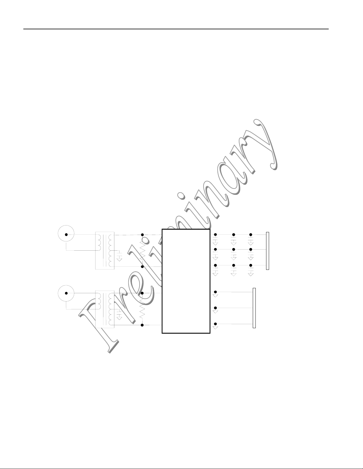
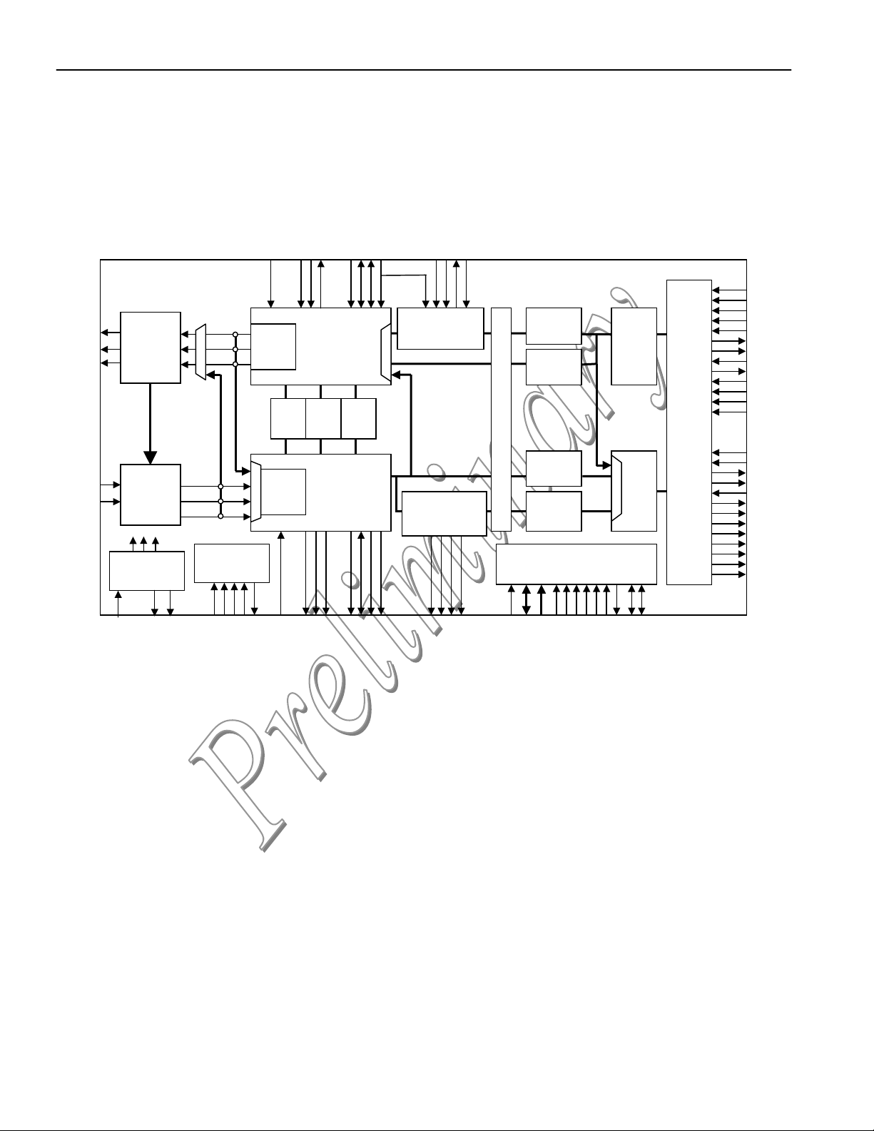
Figure 1-1 shows the external components required at each LIU interface for proper operation. Figure 1-2 shows the functional block diagram of one channel ATM / Packet PHY.
Figure 1-1 LIU External Connections
Transmit
0.05uF
Receive
1:2ct
0.05uF
1:2ct
Each T3/E3 LIU Interface
330
(1%)
330
(1%)
TXP
TXN
RXP
RXN
VDD
VDD
VDD
VSS
VSS
VSS
0.01uF
0.01uF
0.01uF
0.1uF
0.1uF
0.1uF
1uF
3.3V
Power
1uF
Plane
1uF
Ground
Plane
Rev 1.5 3 of 13 022304
Page 4
Maxim/Dallas Semiconductor Confidential Product Preview: DS3181,2,3,4
]
]
A
]
]
A
k
]
]
A
]
]
K
K
[
]
[
]
Figure 1-2 Functional Block Diagram
/ TGCLKn
TDENn
TDATn
TLCLKn
Trail
Trace
Buffer
TSOFn / TIOHMn
TPOHn
TPOHGCLK
Tx
PLCP/FRAC
Formatter
Loopback
Framer Payload
Rx
PLCP/FRAC
Framer
TPOHSOFn
8KREFI
BERT
Tx Cell
Processor
Tx Packet
Processor
Rx Packet
Processor
Rx Cell
Processor
Microprocessor
Interface
System Interface
Loopback
Tx
FIFO
Rx
FIFO
System
Interface
TSCLK
TADR[4:0
TDATA[31:0
TPRTY*
TEN*
TPX
TDXA[4:1
TSOX
TSP
TEOP
TSX
TMOD[1:0
TERR
RSCLK
RADR[4:0
RDATA[31:0
RPRTY*
REN*
RPX
RDXA[4:1
RSOX
REOP
RSX
RVAL
RMOD[1:0
RERR
TDMn
RXPn
RXNn
TXPn
TXNn
DS3/E3
Transmit
LIU
Loopback
LLine Terminal
DS3/E3
Receive
LIU
Clock Rate
Adapter
Loopback
Framer Diagnostic
Line Facility Loopbac
IEEE P1149.1
JTAG Test
Access Port
TMEI
B3ZS/
HDB3
Encoder
HDLC
B3ZS/
HDB3
Decoder
TOHn
TOHGCLKn
TOHSOFn
DS3 / E3
Transmit
Formatter
FEAC
DS3 / E3
Receive
Framer
CLKACLKB
REFCL
JTDI
JTMS
JTDO
JTCL
JTRST*
RECU
ROHn
RDATn
RSOFn
ROHSOFn
ROHGCLKn
RLCLKn
RDENn / RGCLKn
RPOHn
8KREFO
RPOHSOFn
RPOHGCLKn
9:0
CS*
ALE
15:0
A
D
INT*
MOT
RST*
PIOAn
RD*/DS*
WR*/ R/W*
PIOBn
n = port #
2 APPLICATIONS
• Access Concentrators
• Multi-Service Access Platforms
• ATM and Frame Relay Equipment
• Routers and Switches
• SONET/SDH ADM
• SONET/SDH Muxes
• PBXs
• Digital Cross Connect
• PDH Multiplexer/Demultiplexer
• Test Equipment
The following figures, Figure 2-1 and Figure 2-2, show applications for DS3184 as four port unchannelized ATM and packet T3/E3 line cards, respectively.
Rev 1.5 4 of 13 022304
Page 5

Maxim/Dallas Semiconductor Confidential Product Preview: DS3181,2,3,4
R
n
R
R
n
R
Figure 2-1 Four-Port Unchannelized ATM over T3/E3 Line Card
Typical ATM Line Card
Utopia
POS
PHY
2/3
-
-
x
DS3/E3
DS3/E3
Line
Line
DS3154 #1
DS315x #1
4-Chan
4-Chan
DS3/E
DS3/E3
LIU
LIU
Utopia
POS-
DS3164 #1
DS316x #1
4-Chan
4-Chan
DS3/E
DS3/E3
ATM
ATM
PH
PHY
POSPHY
2/3
AT
ATM
Switch
Switch
Card
Card
(S/W+
(S/W+
Igr/Egr Mgt)
Igr/Egr Mgt)
DS318
DS3164 #3
DS316x #3
4-Chan
4-Chan
DS3/E
DS3/E3
ATM
ATM
PH
PHY
X = 1, 2, 3, 4
x
DS3/E3
DS3/E3
Line
Line
DS3154 #3
DS315x #3
4-Chan
4-Chan
DS3/E
DS3/E3
LIU
LIU
Typical ATM Line Card
Figure 2-2 Four-Port Unchannelized HDLC over T3/E3 Line Card
OC -12
OC -
AT
ATM
SA
SA
Typical Packet Line Card
Utopia
POS-
POS-
PHY
2/3
OC -12
OC -
AT
POS
SA
SA
x
DS3/E3
DS3/E3
Line
Line
DS3154 #1
DS315x #1
4-Chan
4-Chan
DS3/E
DS3/E3
LIU
LIU
Utopia
POS-
DS3164 #1
DS316x #1
4-Chan
4-Chan
DS3/E
DS3/E3
ATM
PKT
PH
PHY
POS-
PHY
2/3
AT
IP/PKT
Switch
Switch
Card
Card
(S/W+
(S/W+
Igr/Egr Mgt)
Igr/Egr Mgt)
DS318
DS3164 #3
DS316x #3
4-Chan
4-Chan
DS3/E
DS3/E3
ATM
PH
PHY
X = 1, 2, 3, 4
x
DS3/E3
DS3/E3
Line
Line
DS3154 #3
DS315x #3
4-Chan
4-Chan
DS3/E
DS3/E3
LIU
LIU
Typical Packet Line Card
3 FEATURE DETAILS
The following sections describe the features provided by the DS3184 (quad), DS3183 (triple), DS3182 (dual), and DS3181 (single) PHYs.
Rev 1.5 5 of 13 022304
Page 6

Maxim/Dallas Semiconductor Confidential Product Preview: DS3181,2,3,4
3.1 Global Features
• System interface configurable for UTOPIA 2 / UTOPIA 3 for ATM cell traffic or POS-PHY 2 / POSPHY 3 for HDLC or mixed packet/cell traffic
• Supports the following transmission protocols:
• Direct-mapped ATM over DS3 or subrate DS3
• PLCP-mapped ATM over DS3
• Direct-mapped ATM over G.751 E3 or subrate G.751 E3
• PLCP-mapped ATM over G.751 E3
• Direct-mapped ATM over G.832 E3 or subrate G.832 E3
• Direct-mapped ATM over externally-defined frame formats up to 52 Mbps
• Clear-channel ATM (cell-based physical layer) at line rates up to 52 Mbps
• Direct-mapped HDLC over DS3 or subrate DS3
• Direct-mapped HDLC over G.751 E3 or subrate G.751 E3
• Direct-mapped HDLC over G.832 E3 or subrate G.832 E3
• Direct-mapped HDLC over externally-defined frame formats up to 52 Mbps
• Clear-channel HDLC at line rates up to 52 Mbps
• In UTOPIA bus mode, ports are independently configurable for any ATM protocol
• In POS-PHY bus mode, ports are independently configurable for any ATM or HDLC protocol
• Provides all necessary I/O to support externally controlled subrate DS3 or E3 on any ports
• Supports gapped 52 MHz clock rates for signals embedded in SONET/SDH
• Clock, data and control signals can be inverted to allow a glueless interface to other devices
• Detection of loss of transmit clock and loss of receive clock
• Manual or automatic one-second update of performance monitoring counters
• Each port can be put into a low-power standby mode when not being used
3.2 Receive DS3/E3 LIU Features
• AGC/Equalizer block handles from 0 dB to 15 dB of cable loss
• Loss-of-lock PLL status indication
• Interfaces directly to a DSX monitor signal (20 dB flat loss) using built-in pre-amp
• Digital and analog Loss of Signal (LOS) detectors (ANSI T1.231 and ITU G.775)
• Per-channel power-down control
3.3 Receive DS3/E3 Framer Features
• Frame synchronization for M23 or C-bit Parity DS3, G.751 E3 or G.832 E3
• B3ZS/HDB3 decoding
• Detection and accumulation of bipolar violations (BPV), code violations (CV), excessive zeroes
occurrences (EXZ), F-bit errors, M-bit errors, FAS errors, LOF occurrences, P-bit parity errors, CPbit parity errors, BIP-8 errors, and far end block errors (FEBE)
• Detection of RDI, AIS, DS3 idle signal, loss of signal (LOS), severely error framing event (SEFE),
change of frame alignment (COFA), receipt of B3ZS/HDB3 codewords, DS3 application ID bit, DS3
M23/C-bit format mismatch, G.751 national bit, and G.832 RDI (FERF), payload type, and timing
marker bits
• HDLC controller with 256 byte FIFO for DS3 path maintenance data link (PMDL), G.751 national bit, or G.832 NR/GC channels
• FEAC controller with four-codeword FIFO for DS3 FEAC channel
• 16-byte Trail Trace Buffer compares and stores G.832 trail access point identifier
Rev 1.5 6 of 13 022304
Page 7

Maxim/Dallas Semiconductor Confidential Product Preview: DS3181,2,3,4
• C bits configurable as payload or overhead
• Most framing overhead fields presented on the receive overhead port
• Framer pass-through mode for clear channel applications and externally defined frame formats
• Built-in support for subrate DS3/E3
3.4 Receive PLCP Framer Features
• PLCP frame synchronization
• C1 cycle/stuff counter interpretation
• Detection of out of frame (OOF), BIP-8 errors, FEBE and RAI (Yellow Signal)
• Frame timing is presented on the 8KREFO output pin
• All path overhead fields presented on the PLCP receive overhead port
3.5 Receive Cell Processor Features
• HEC-based cell delineation within the DS3/E3 frame, the PLCP frame, an externally defined frame, or the entire line bandwidth
• Cell descrambling using the self-synchronizing scrambler (x43+1) for ATM over DS3/E3 or the
distributed sample scrambler for clear-channel ATM (cell-based physical layer)
• HEC error detection and correction; HEC discard
• Filtering of idle, unassigned and/or invalid cells (provisionable)
• Header pattern comparison vs. 32-bit header pattern and mask registers; counting of matching or non-
matching cells; discard of matching or non-matching cells
• Four-cell Receive FIFO
• Controls include enables/disables/settings for: cell processing, coset polynomial addition, error
correction, erred cell extraction, cell descrambling, idle/unassigned/invalid cell filtering, header
pattern match counting/discarding, LCD integration time
• Status fields include: out of cell delineation (OCD), loss of cell delineation (LCD) and receipt of idle, unassigned, invalid, erred, corrected or header-pattern-match cells
• Performance monitoring counters for forwarded cells, corrected cells, uncorrectable cells, header pattern match/no-match cells, and filtered idle/unassigned/invalid cells
3.6 Receive Packet Processor Features
• Packet descrambling using the self-synchronizing scrambler (x43+1)
• Flag detection, packet delineation, and interframe fill discard (flags and all-ones)
• Packet abort detection and accumulation
• Bit or octet destuffing
• FCS checking (16-bit or 32-bit), error accumulation, and FCS discard
• Packet size checking vs. programmable minimum and maximum size registers
• Abort declaration for packets with non-integral number of bytes
• Controls include enables/disables/settings for: packet processing, descrambling, 16/32-bit FCS,
filtering of FCS erred packets, FCS discard, minimum/maximum packet size
• Status fields include: receipt of FCS erred packet, aborted packet, size violation packet, non-integerlength packets
• Performance monitoring counters for forwarded packets, forwarded bytes, aborted bytes, FCS erred packets, aborted packets, size violation packets (min, max, non-integer-length)
Rev 1.5 7 of 13 022304
Page 8

Maxim/Dallas Semiconductor Confidential Product Preview: DS3181,2,3,4
3.7 Receive FIFO Features
• Storage capacity for four cells or 256 bytes of packet data
• Programmable port address
• Programmable fill level thresholds
• Underflow and overflow status indications
3.8 Receive System Interface Features
• UTOPIA 2 / UTOPIA 3 interface in cell mode, POS-PHY 2 / POS-PHY 3 interface in packet or mixed traffic modes
• 8, 16, or 32 bit data bus at clock rates from 10 MHz to 66 MHz
• Polled and direct cell available outputs
• Controls include enables/disables/settings for: HEC transfer, signal inversions, parity enable/polarity,
cell available desertion time
3.9 Transmit System Interface Features
• UTOPIA 2 / UTOPIA 3 interface in cell mode, POS-PHY 2 / POS-PHY 3 interface in packet or mixed traffic modes
• 8, 16, or 32 bit data bus at clock rates from 10 MHz to 66 MHz
• Polled and direct cell available outputs
• Controls include enables/disables/settings for: HEC transfer, signal inversions, parity enable/polarity,
cell available desertion time
3.10 Transmit FIFO Features
• Storage capacity for four cells or 256 bytes of packet data
• Programmable port address
• Programmable fill level thresholds
• Underflow and overflow status indications
3.11 Transmit Cell Processor Features
• Programmable fill cell type
• HEC calculation and insertion/overwrite, including coset addition
• Cell scrambling using the self-synchronizing scrambler (x
distributed sample scrambler for clear-channel ATM (cell-based physical layer)
• Single-bit and multiple-bit header error insertion for diagnostics
• Controls include enables/disables/settings for: cell processing, HEC insertion, coset polynomial
addition, cell scrambling, fill cell type, error insertion type/rate/count, HEC bit corruption
• Counter for number of cells read from the transmit FIFO
• Cell mapping into the DS3/E3 frame, the PLCP frame, an externally defined frame, or the entire line
bandwidth
43
+1) for ATM over DS3/E3 or the
3.12 Transmit Packet Processor Features
• FCS calculation (16-bit or 32-bit) and insertion/overwrite
• Programmable FCS error insertion for diagnostics
• Bit or octet stuffing
• Programmable inter-frame fill insertion (flags or all-ones)
Rev 1.5 8 of 13 022304
Page 9

Maxim/Dallas Semiconductor Confidential Product Preview: DS3181,2,3,4
• Automatic packet abort insertion
43
• Packet scrambling using the self-synchronizing scrambler (x
+1)
• Controls include enables/disables/settings for: packet processing, FCS insertion or overwrite, 16/32bit FCS, inter-frame fill type/length, scrambling, FCS error insertion type/rate/count
• Counters for number of packets and bytes read from the transmit FIFO
3.13 Transmit PLCP Formatter Features
• Insertion of FAS bytes (A1, A2), path overhead identification (POI) bytes, and path overhead bytes
• Generation of BIP-8 (B1), FEBE and RAI (G1)
• C1 cycle/stuff counter generation referenced to the 8KREFI input pin, referenced to the received
PLCP timing, or based on a fixed stuff pattern
• Automatic or manual insertion of FAS errors, BIP-8 errors
• All path overhead fields can be sourced from the PLCP transmit overhead port
3.14 Transmit DS3/E3 Formatter Features
• Insertion of framing overhead for M23 or C-bit parity DS3, G.751 E3 or G.832 E3
• B3ZS/HDB3 encoding
• Generation of RDI, AIS, DS3 idle signal, and G.832-E3 RDI
• Automatic or manual insertion of bipolar violations (BPVs), excessive zeroes (EXZ) occurrences, F-
bit errors, M-bit errors, FAS errors, P-bit parity errors, CP-bit parity errors, BIP-8 errors, and far end
block errors (FEBE)
• HDLC controller with 256 byte FIFO for DS3 path maintenance data link (PMDL), G.751 national bit, or G.832 NR or GC channels
• FEAC controller for DS3 FEAC channel can be configured to send one codeword, one codeword continuously, or two different codewords back-to-back to send DS3 Line Loopback commands
• 16-byte Trail Trace Buffer sources the G.832 trail access point identifier
• Insertion of G.832 payload type and timing marker bits from registers
• C bits configurable as payload or overhead; as overhead they can be controlled from registers or the
transmit overhead port
• Most framing overhead fields can be sourced from transmit overhead port
• Formatter pass-through mode for clear channel applications and externally defined frame formats
• Built-in support for subrate DS3/E3
3.15 Transmit DS3/E3 LIU Features
• Wide 50±20% transmit clock duty cycle
• Line Build-Out (LBO) control
• Tri-state line driver outputs support protection switching applications
• Per-channel power-down control
• Output driver monitor
3.16 HDLC Controller Features
• 256-byte receive and transmit FIFOs
• Handles all of the normal Layer 2 tasks including zero stuffing/destuffing, FCS generation/checking,
abort generation/checking, flag generation/detection, and byte alignment
• Programmable high or low water marks for the transmit and receive FIFOs
Rev 1.5 9 of 13 022304
Page 10

Maxim/Dallas Semiconductor Confidential Product Preview: DS3181,2,3,4
• Terminates the Path Maintenance Data Link in DS3 C-bit Parity mode or the G.751 Sn bit or the G.832 NR or GC channels
3.17 FEAC Controller Features
• Designed to handle multiple FEAC codewords without Host intervention
• Receive FEAC automatically validates incoming codewords and stores them in a 4-codeword FIFO
• Transmit FEAC can be configured to send one codeword, one codeword continuously, or two
different codewords back-to-back to send DS3 Line Loopback commands
• Terminates the FEAC channel in DS3 C-Bit Parity mode or the Sn bit in E3 mode
3.18 Trail Trace Buffer Features
• Extraction and storage of the incoming G.832 trail access point identifier in a 16-byte receive register
• Insertion of the outgoing trail access point identifier from a 16-byte transmit register
• Receive trace identifier unstable status indication
3.19 Bit Error Rate Tester (BERT) Features
• Generates and detects pseudo-random patterns and repetitive patterns from 1 to 32 bits in length
• Supports pattern insertion/extraction in PLCP payload, DS3/E3 payload, or entire data stream
• Large 24-bit error counter allows testing to proceed for long periods without host intervention
• Errors can be inserted in the generated BERT patterns for diagnostic purposes (single bit errors or
specific bit-error rates)
3.20 Jitter Attenuator Features
• Fully integrated, requires no external components
• Standards-compliant jitter attenuation/jitter transfer
• Can be inserted into the receive path or the transmit path
• 16-bit buffer depth
3.21 Loopback Features
• Line terminal loopback (transmit to receive)
• Line facility loopback (receive to transmit) with optionally transmitting unframed all-one payload
toward system/trunk interface
• Framer diagnostic loopback (transmit to receive) with optionally transmitting unframed all-one signal toward line/tributary interface
• Simultaneous line facility loopback and framer diagnostic loopback
• Framer payload loopback (receive to transmit) with optionally transmitting unframed all-one payload
toward system/trunk interface
• System interface loopback (transmit to receive)
3.22 Microprocessor Interface Features
• Multiplexed or non-multiplexed 8 or 16-bit control port
• Intel and Motorola bus compatible
• Global reset input pin
• Global interrupt output pin
• Two programmable I/O pins per port
Rev 1.5 10 of 13 022304
Page 11

Maxim/Dallas Semiconductor Confidential Product Preview: DS3181,2,3,4
B
3.23 Subrate Features
• Independent per port built-in support for subrate DS3 or E3
• Independent subrate operation for both Rx and Tx data paths
• Subrate operation for each channel is totally independent from the other channels’ operation, i.e. all
subrate functions within the device are mutually exclusive
• Three distinct subrate algorithms:
• (FFRAC) Externally controlled with DS3 or E3 payload manipulating capability
• (XFRAC) Externally controlled with simple DS3 or E3 data rate reduction capability
• (IFRAC) Internally controlled with flexible DS3 or E3 data rate reduction capability
• Subrate algorithm selection is on per port basis
• Internal subrate mechanism allows down to bit-level granularity of the DS3 or E3 payload
4 STANDARDS COMPLIANCE
Specification
ANSI
T1.102-1993
T1.107-1995
T1.231-1997
Specification Title
Digital Hierarchy – Electrical Interfaces
Digital Hierarchy – Formats Specification
Digital Hierarchy – Layer 1 In-Service Digital Transmission Performance
Monitoring
T1.404-1994
T1.646-1995
Network-to-Customer Installation – DS3 Metallic Interface Specification
Broadband ISDN – Physical Layer Specification for User-Network Interfaces
Including DS1/ATM
ATM Forum af-phy-0034.000 E3 Public UNI, August, 1995 af-phy-0039.000 UTOPIA Level 2, Version 1.0, June, 1995 af-phy-0043.000
A Cell-Based Transmission Convergence Sublayer for Clear Channel Interfaces,
November, 1995
af-phy-0054.000 DS3 Physical Layer Interface Specification, January, 1996
af-phy-0136.000 UTOPIA 3 Physical Layer Interface, November, 1999
af-phy-0143.000 Frame-based ATM Interface (Level 3), March, 2000
af-bici-0013.003
BISDN Inter Carrier Interface (B-ICI) Specification Version 2.0 (Integrated),
December, 1995 ETSI
ETS 300 686
Business TeleCommunications; 34Mbps and 140Mbits/s digital leased lines (D34U,
D34S, D140U and D140S); Network interface presentation, 1996
ETS 300 687
Business TeleCommunications; 34Mbps digital leased lines (D34U and D34S);
Connection characteristics, 1996
TBR 24
Business TeleCommunications; 34Mbps digital unstructured and structured lease
lines; attachment requirements for terminal equipment interface, 1997
ETS 300 337
Transmission and Multiplexing (TM); Generic frame structures for the transport of
various signals (including Asynchronous Transfer Mode (ATM) cells and
Synchronous Digital Hierarchy (SDH) elements) at the ITU-T Recommendation
G.702 hierarchical rates of 2 048 kbit/s, 34 368 kbit/s and 139 264 kbit/s, Second
Edition, June, 1997
ETS 300 689
usiness TeleCommunications (BTC); 34 Mbps digital leased lines (D34U and
Rev 1.5 11 of 13 022304
Page 12

Maxim/Dallas Semiconductor Confidential Product Preview: DS3181,2,3,4
Specification
Specification Title
D34S), Terminal equipment interface, V 1.2.1, 2001-07
IEEE
IEEE Std 11491990 IETF
IEEE Standard Test Access Port and Boundary-Scan Architecture, (Includes IEEE
Std 1149-1993) October 21, 1993
RFC 1661 The Point-to-Point Protocol (PPP), July, 1994 RFC 1662 PPP in HDLC-like Framing, July, 1994 RFC 2496 Definition of Managed Objects for the DS3/E3 Interface Type, January, 1999
ISO
ISO 3309:1993
Information Technology – Telecommunications & information exchange between
systems – High Level Data Link Control (HDLC) procedures – Frame structure,
Fifth Edition, 1993 ITU-T G.703 Physical/Electrical Characteristics of Hierarchical Digital Interfaces, 1991 G.704
Synchronous Frame Structures Used at 1544, 6312, 2048, 8488 and 44 736 kbit/s
Hierarchical Levels, July, 1995
G.751
Digital Multiplex Equipment Operating at the Third Order Bit Rate of 34,368 kbit/s
and the Fourth Order bit Rate of 139,264 kbit/s and Using Positive Justification,
1993
G.775
Loss Of Signal (LOS) and Alarm Indication Signal (AIS) Defect Detection and
Clearance Criteria, November, 1994
G.804 ATM Cell Mapping Into Plesiochronous Digital Hierarchy (PDH), November, 1993 G.823
The Control of Jitter and Wander Within Digital Networks Which are Based on the
2048 kbit/s Hierarchy, 1993
G.832
Transport of SDH Elements on PDH Networks – Frame and Multiplexing
Structures, November, 1995
I.432 B-ISDN User-Network Interface – Physical Layer Specification, March, 1993 O.151
Error Performance Measuring Equipment Operating at the Primary Rate and
Above, October, 1992 Q.921 ISDN User-Network Interface – Data Link Layer Specification, March 1993
OIF
OIF-SPI3-01.0
System Packet Interface Level 3 (SPI-3): OC-48 System Interface for Physical and
Link Layer Devices
Saturn Group POS-PHY 2 POS-PHYTM Level 2 Packet Over SONET Interface Specification for Physical Layer
Devices, December, 1998
POS-PHY 3
POS-PHY Level 3 Packet Over SONET Interface Specification for Physical and Link
Layer Devices, June, 2000
Telcordia
GR-253-CORE SONET Transport Systems: Common Generic Criteria, Issue 2, December 1995 GR-499-CORE Transport Systems Generic Requirements (TSGR): Common Requirements, Issue 2,
December 1998
GR-820-CORE Generic Digital Transmission Surveillance, Issue 1, November 1994
Saturn and POS-PHY are trademarks of PMC-Sierra, Inc.
Rev 1.5 12 of 13 022304
Page 13

Maxim/Dallas Semiconductor Confidential Product Preview: DS3181,2,3,4
5 PACKAGE MECHANICAL DIMENSIONS
The target package is a 27x27 mm 400-lead TE1-CSBGA with ball pitch of 1.27mm for all port density
configuration.
6 POWER ESTIMATE
Current typical power estimate is 2.7 Watts at 3.3V (pending mode of operation).
1
TE-CSBGA: Thermally Enhanced Chip Scale Ball Grid Array
Rev 1.5 13 of 13 022304
 Loading...