

Page 1
TL/F/5816
DS1631/DS3631/DS1632/DS3632/DS1633/DS3633/DS1634/DS3634
CMOS Dual Peripheral Drivers
July 1992
DS1631/DS3631/DS1632/DS3632/DS1633/DS3633/
DS1634/DS3634 CMOS Dual Peripheral Drivers
General Description
The DS1631 series of dual peripheral drivers was designed
to be a universal set of interface components for CMOS
circuits.
Each circuit has CMOS compatible inputs with thresholds
that track as a function of V
CC
(approximately (/2 VCC). The
inputs are PNPs providing the high impedance necessary
for interfacing with CMOS.
Outputs have high voltage capability, minimum breakdown
voltage is 56V at 250 mA.
The outputs are Darlington connected transistors. This allows high current operation (300 mA max) at low internal
V
CC
current levels since base drive for the output transistor
is obtained from the load in proportion to the required loading conditions. This is essential in order to minimize loading
on the CMOS logic supply.
Typical V
CC
e
5V power is 28 mW with both outputs ON.
V
CC
operating range is 4.5V to 15V.
The circuit also features output transistor protection if the
V
CC
supply is lost by forcing the output into the high impe-
dance OFF state with the same breakdown levels as when
V
CC
was applied.
Pin-outs are the same as the respective logic functions
found in the following popular series of circuits: DS75451,
DS75461. This feature allows direct conversion of present
systems to the MM74C CMOS family and DS1631 series
circuits with great power savings.
The DS1631 series is also TTL compatible at V
CC
e
5V.
Features
Y
CMOS compatible inputs
Y
High impedance inputs PNP’s
Y
High output voltage breakdown 56V min
Y
High output current capability 300 mA max
Y
Same pin-outs and logic functions as DS75451 and
DS75461 series circuits
Y
Low VCCpower dissipation (28 mW both outputs ‘‘ON’’
at 5V)
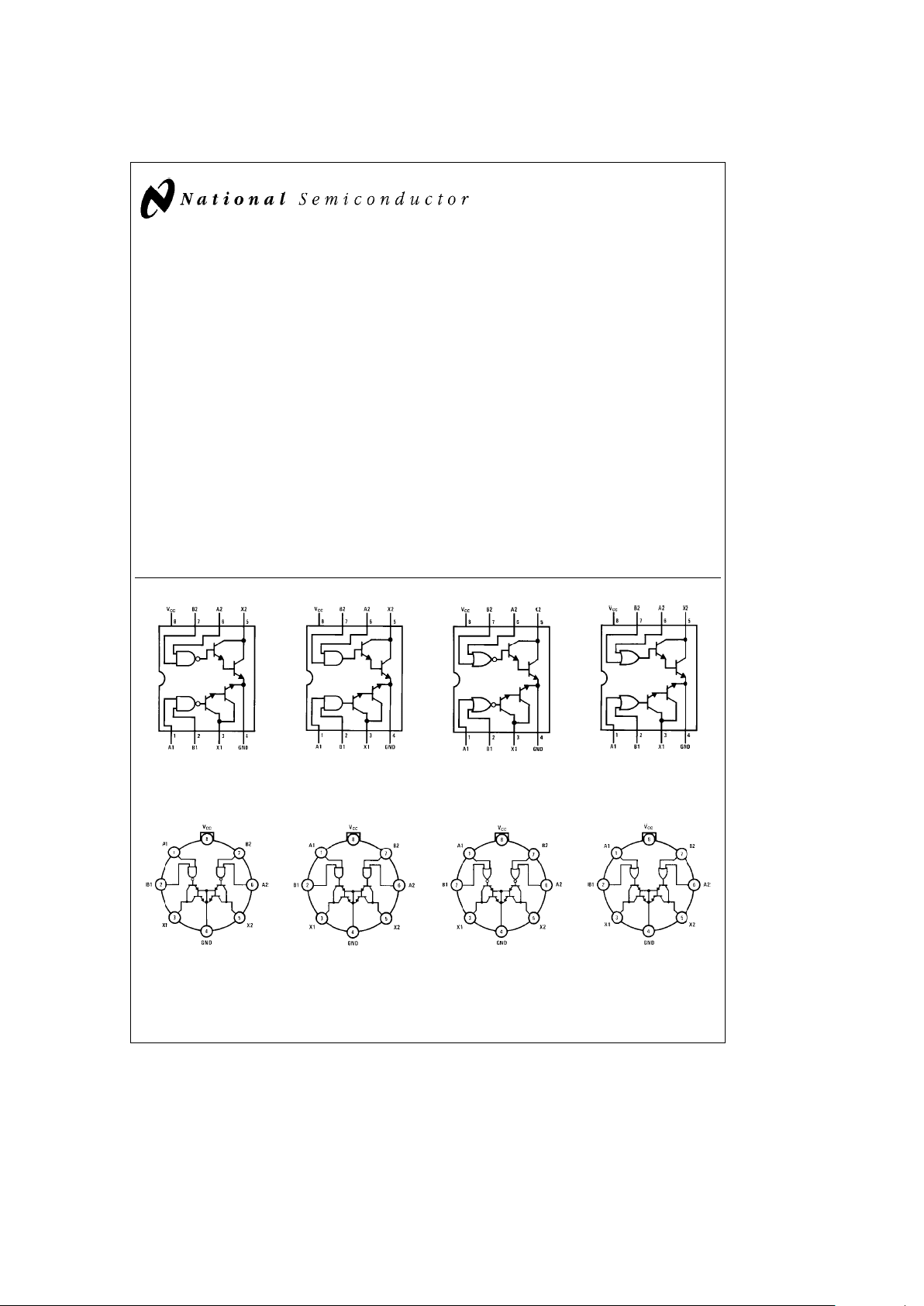
Connection Diagrams (Dual-In-Line and Metal Can Packages)
TL/F/5816– 1
Top View
Order Number DS1631J-8
or DS3631N
TL/F/5816– 2
Top View
Order Number DS1632J-8
or DS3632N
TL/F/5816– 3
Top View
Order Number DS1633J-8
or DS3633N
TL/F/5816– 4
Top View
Order Number DS1634J-8
or DS3634N
See NS Package Number J08A or N08E
TL/F/5816– 5
Top View
(Pin 4 is electrically connected to the
case.)
Order Number DS1631H
TL/F/5816– 6
Top View
(Pin 4 is electrically connected to the
case.)
Order Number DS1632H
TL/F/5816– 7
Top View
(Pin 4 is electrically connected to the
case.)
Order Number DS1633H
TL/F/5816– 8
Top View
(Pin 4 is electrically connected to the
case.)
Order Number DS1634H
See NS Package Number H08C
C
1995 National Semiconductor Corporation RRD-B30M105/Printed in U. S. A.
Page 2
Absolute Maximum Ratings (Note 1)
If Military/Aerospace specified devices are required,
please contact the National Semiconductor Sales
Office/Distributors for availability and specifications.
Supply Voltage 16V
Voltage at Inputs
b
0.3V to V
CC
a
0.3V
Output Voltage 56V
Storage Temperature Range
b
65§Ctoa150§C
Maximum Power Dissipation* at 25§C
Cavity Package 1133 mW
Molded Package 1022 mW
TO-5 Package 787 mW
Lead Temperature (Soldering, 4 sec. 260
§
C
*Derate cavity package 7.6 mW/§C above 25§C; derate molded package
8.2 mW/
§
C above 25§C; derate TO-5 package 5.2 mW/§C above 25§C.
Operating Conditions
Min Max Units
Supply Voltage, V
CC
DS1631/DS1632/ 4.5 15 V
DS1633/DS1634
DS3631/DS3632/ 4.75 15 V
DS3633/DS3634
Temperature, T
A
DS1631/DS1632/
b
55
a
125
§
C
DS1633/DS1634
DS3631/DS3632/ 0
a
70
§
C
DS3633/DS3634
Electrical Characteristics (Notes 2 and 3)
Symbol Parameter Conditions Min Typ Max Units
ALL CIRCUITS
V
IH
Logical ‘‘1’’ Input Voltage (
Figure 1
)V
CC
e
5V 3.5 2.5 V
V
CC
e
10V 8.0 5 V
V
CC
e
15V 12.5 7.5 V
V
IL
Logical ‘‘0’’ Input Voltage (
Figure 1
)V
CC
e
5V 2.5 1.5 V
V
CC
e
10V 5.5 2.0 V
V
CC
e
15V 7.5 2.5 V
I
IH
Logical ‘‘1’’ Input Current V
CC
e
15V, V
IN
e
15V, (
Figure 2
) 0.1 10 mA
I
IL
Logical ‘‘0’’ Input Current V
IN
e
0.4V, (
Figure 3
)V
CC
e
5V
b50b
120 m A
V
CC
e
15V
b
200b360 m A
V
OH
Output Breakdown Voltage V
CC
e
15V, I
OH
e
250 mA, (
Figure 1
)5665V
V
OL
Output Low Voltage V
CC
e
Min, (
Figure 1
),
DS1631, DS1632, I
OL
e
100 mA 0.85 1.1 V
DS1633, DS1634
I
OL
e
300 mA 1.1 1.4 V
V
CC
e
Min, (
Figure 1
),
DS3631, DS3632, I
OL
e
100 mA 0.85 1.0 V
DS3633, DS3634
I
OL
e
300 mA 1.1 1.3 V
DS1631/DS3631
I
CC(0)
Supply Currents V
IN
e
0V, (
Figure 4)
V
CC
e
5V Output Low 7 11 mA
V
CC
e
15V Both Drivers 14 20 mA
I
CC(1)
(
Figure 4
)V
CC
e
5V, V
IN
e
5V Output High 2 3 mA
V
CC
e
15V, V
IN
e
15V Both Drivers 7.5 10 mA
t
PD1
Propagation to ‘‘1’’ V
CC
e
5V, T
A
e
25§C, C
L
e
15 pF, R
L
e
50X,V
L
e
10V,
500 ns
(
Figure 5
)
t
PD0
Propagation to ‘‘0’’ V
CC
e
5V, T
A
e
25§C, C
L
e
15 pF, R
L
e
50X,V
L
e
10V,
750 ns
(
Figure 5
)
DS1632/DS3632
I
CC(0)
Supply Currents (
Figure 4
)V
CC
e
5V, V
IN
e
5V
Output Low
812mA
V
CC
e
15V, V
IN
e
15V 18 23 mA
I
CC(1)
V
IN
e
0V, (
Figure 4
)V
CC
e
5V
Output High
2.5 3.5 mA
V
CC
e
15V 9 14 mA
t
PD1
Propagation to ‘‘1’’ V
CC
e
5V, T
A
e
25§C, C
L
e
15 pF, R
L
e
50X,V
L
e
10V,
500 ns
(
Figure 5
)
t
PD0
Propagation to ‘‘0’’ V
CC
e
5V, T
A
e
25§C, C
L
e
15 pF, R
L
e
50X,V
L
e
10V,
750 ns
(
Figure 5
)
2
Page 3
Electrical Characteristics (Notes 2 and 3) (Continued)
Symbol Parameter Conditions Min Typ Max Units
DS1633/DS3633
I
CC(0)
Supply Currents V
IN
e
0V, (
Figure 4
)V
CC
e
5V Output Low 7.5 12 mA
V
CC
e
15V 16 23 mA
I
CC(1)
(
Figure 4
)V
CC
e
5V, V
IN
e
5V Output High 2 4 mA
V
CC
e
15V, V
IN
e
15V 7.2 15 mA
t
PD1
Propagation to ‘‘1’’ V
CC
e
5V, T
A
e
25§C, C
L
e
15 pF, R
L
e
50X,V
L
e
10V,
500 ns
(
Figure 5
)
t
PD0
Propagation to ‘‘0’’ V
CC
e
5V, T
A
e
25§C, C
L
e
15 pF, R
L
e
50X,V
L
e
10V,
750 ns
(
Figure 5
)
DS1634/DS3634
I
CC(0)
Supply Currents (
Figure 4
)V
CC
e
5V, V
IN
e
5V Output Low 7.5 12 mA
V
CC
e
15V, V
IN
e
15V 18 23 mA
I
CC(1)
V
IN
e
0V, (
Figure 4
)V
CC
e
5V Output High 3 5 mA
V
CC
e
15V 11 18 mA
t
PD1
Propagation to ‘‘1’’ V
CC
e
5V, T
A
e
25§C, C
L
e
15 pF, R
L
e
50X,V
L
e
10V,
500 ns
(
Figure 5
)
t
PD0
Propagation to ‘‘0’’ V
CC
e
5V, T
A
e
25§C, C
L
e
15 pF, R
L
e
50X,V
L
e
10V,
750 ns
(
Figure 5
)
Note 1: ‘‘Absolute Maximum Ratings’’ are those values beyond which the safety of the device cannot be guaranteed. Except for ‘‘Operating Temperature Range’’
they are not meant to imply that the devices should be operated at these limits. The table of ‘‘Electrical Characteristics’’ provides conditions for actual device
operation.
Note 2: Unless otherwise specified min/max limits apply across the
b
55§Ctoa125§C temperature range for the DS1631, DS1632, DS1633 and DS1634 and
across the 0
§
Ctoa70§C range for the DS3631, DS3632, DS3633 and DS3634. All typical values are for T
A
e
25§C.
Note 3: All currents into device pins shown as positive, out of device pins as negative, all voltages referenced to ground unless otherwise noted. All values shown
as max or min on absolute value basis.
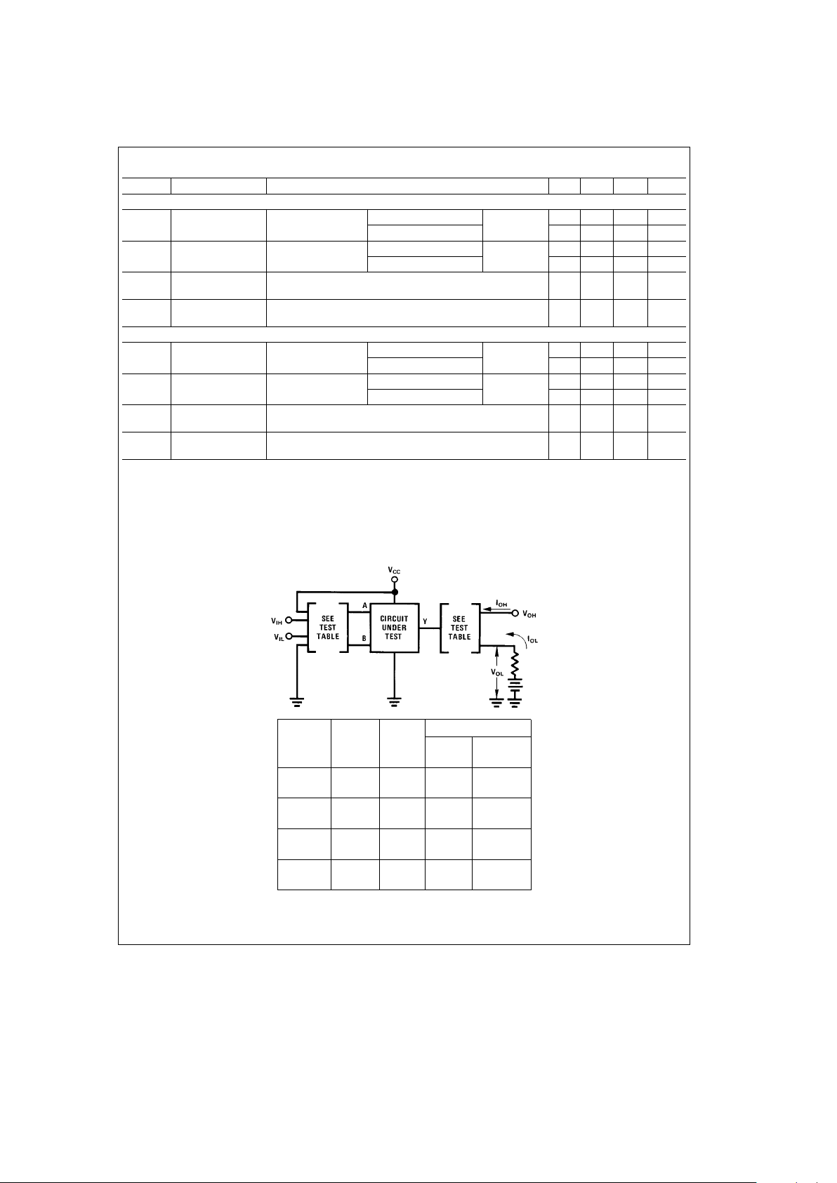
Test Circuits
TL/F/5816– 9
Input
Other
Output
Circuit Under
Input
Apply Measure
Test
DS3631 V
IH
V
IH
I
OH
V
OH
V
IL
V
CC
I
OL
V
OL
DS3632 V
IH
V
IH
I
OL
V
OL
V
IL
V
CC
I
OH
V
OH
DS3633 V
IH
GND I
OH
V
OH
V
IL
V
IL
I
OL
V
OL
DS3634 V
IH
GND I
OL
V
OL
V
IL
V
IL
I
OH
V
OH
Note: Each input is tested separately.
FIGURE 1. VIH,VIL,VOH,V
OL
3
Page 4

Test Circuits (Continued)
TL/F/5816– 10
Each input is tested separately.
FIGURE 2. I
IH
TL/F/5816– 11
Note A: Each input is tested separately.
Note B: When testing DS1633 and DS1634 input not under test is grounded.
For all other circuits it is at V
CC
.
FIGURE 3. I
IL
TL/F/5816– 12
Both gates are tested simultaneously.
FIGURE 4. ICCfor AND and NAND Circuits
Schematic Diagram (Equivalent Circuit)
TL/F/5816– 15
4
Page 5

Switching Time Waveforms
TL/F/5816– 13
TL/F/5816– 14
Note 1: The pulse generator has the following characteristics: PRRe500 kHz, Z
OUT
&
50X
Note 2: C
L
includes probe and jig capacitance
FIGURE 5. Switching Times
5
Page 6

Physical Dimensions inches (millimeters)
Metal Can Package (H)
Order Number DS1631H, DS1632H, DS1633H or DS1634H
NS Package Number H08C
6
Page 7

Physical Dimensions inches (millimeters) (Continued)
Ceramic Dual-In-Line Package (J)
Order Number DS1631J-8, DS1632J-8, DS1633J-8 or DS1634J-8
NS Package Number J08A
7
Page 8

DS1631/DS3631/DS1632/DS3632/DS1633/DS3633/DS1634/DS3634
CMOS Dual Peripheral Drivers
Physical Dimensions inches (millimeters) (Continued)
Molded Dual-In-Line Package (N)
Order Number DS3631N, DS3632N,
DS3633N and DS3634N
NS Package Number N08E
LIFE SUPPORT POLICY
NATIONAL’S PRODUCTS ARE NOT AUTHORIZED FOR USE AS CRITICAL COMPONENTS IN LIFE SUPPORT
DEVICES OR SYSTEMS WITHOUT THE EXPRESS WRITTEN APPROVAL OF THE PRESIDENT OF NATIONAL
SEMICONDUCTOR CORPORATION. As used herein:
1. Life support devices or systems are devices or 2. A critical component is any component of a life
systems which, (a) are intended for surgical implant support device or system whose failure to perform can
into the body, or (b) support or sustain life, and whose be reasonably expected to cause the failure of the life
failure to perform, when properly used in accordance support device or system, or to affect its safety or
with instructions for use provided in the labeling, can effectiveness.
be reasonably expected to result in a significant injury
to the user.
National Semiconductor National Semiconductor National Semiconductor National Semiconductor
Corporation Europe Hong Kong Ltd. Japan Ltd.
1111 West Bardin Road Fax: (
a
49) 0-180-530 85 86 13th Floor, Straight Block, Tel: 81-043-299-2309
Arlington, TX 76017 Email: cnjwge@tevm2.nsc.com Ocean Centre, 5 Canton Rd. Fax: 81-043-299-2408
Tel: 1(800) 272-9959 Deutsch Tel: (
a
49) 0-180-530 85 85 Tsimshatsui, Kowloon
Fax: 1(800) 737-7018 English Tel: (
a
49) 0-180-532 78 32 Hong Kong
Fran3ais Tel: (
a
49) 0-180-532 93 58 Tel: (852) 2737-1600
Italiano Tel: (
a
49) 0-180-534 16 80 Fax: (852) 2736-9960
National does not assume any responsibility for use of any circuitry described, no circuit patent licenses are implied and National reserves the right at any time without notice to change said circuitry and specifications.
 Loading...