

Page 1

May 2007
DS15EA101
0.15 to 1.5 Gbps Adaptive Cable Equalizer with LOS
Detection
General Description
The DS15EA101 is an adaptive equalizer optimized for equalizing data transmitted over copper cables. The DS15EA101
operates over a wide range of data rates from 150 Mbps to
1.5+ Gbps and automatically adapts to equalize any cable
length from zero meters to lengths that attenuate the signal
by 35 dB at 750 MHz.
The DS15EA101 allows either single-ended or differential input drive. This enables equalization of coaxial cables as well
as differential twin-ax and twisted pair cables.
Additional features include an LOS output and an output enable which, when tied together, disable the output when no
signal is present.
The DS15EA101 is powered from a single 3.3V supply and
consumes 210 mW at 1.5 Gbps. It operates over the full
−40°C to +85°C industrial temperature range and is available
in a space saving 4 x 4 mm LLP-16 package which allows for
high density placement of components in multi-channel applications.
Features
■
Automatic equalization of coaxial, twin-ax and twisted pair
cables
■
High data rates: 150 Mbps to 1.5+ Gbps
■
Up to 35 dB of boost at 750 MHz
■
LOS detection and output enable
■
Single-ended or differential input
■
50Ω differential outputs
■
Low power operation, 210 mW (typ) at 1.5 Gbps
■
Industrial -40°C to +85°C temperature
■
Space-saving 4 x 4 mm LLP-16 package
Applications
■
Cable extention applications
■
Security cameras
■
Remote LCDs and LED panels
■
Data recovery equalization
Typical Application
20201701
© 2007 National Semiconductor Corporation 202017 www.national.com
DS15EA101 0.15 to 1.5 Gbps Adaptive Cable Equalizer with LOS Detection
Page 2

Absolute Maximum Ratings (Note 1)
Supply Voltage −0.5V to 3.6V
Input Voltage (all inputs) −0.3V to VCC+0.3V
Storage Temperature Range −65°C to +150°C
Junction Temperature +150°C
Lead Temperature
(Soldering 4 Sec) +260°C
Package Thermal Resistance
θJASQA16A
θJC SQA16A
+42.1°C/W
+8.2°C/W
ESD Rating (HBM) 8 kV
ESD Rating (MM) 250V
Recommended Operating
Conditions
Supply Voltage (VCC ) 3.3V ±5%
Input Coupling Capacitance 1.0 µF
Loop Capacitor (Connected between
CAP+ and CAP-) 1.0 µF
Operating Free Air Temperature (TA) -40°C to +85°C
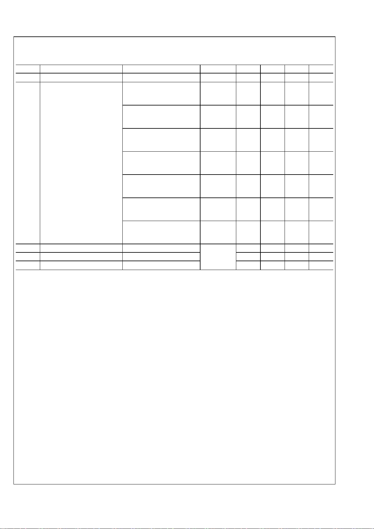
DC Electrical Characteristics
Over Supply Voltage and Operating Temperature ranges, unless otherwise specified (Notes 2, 3).
Symbol Parameter Conditions Reference Min Typ Max Units
V
CM
Input Common Mode Voltage IN+, IN-
1.9 V
V
ID
Input Voltage At DS15EA101 input
(Notes 4, 6)
720 800 950
mV
P−P
V
OS
Output Common Mode Voltage
OUT+, OUT-
VCC –
V
OUT
/2
V
V
OUT
Output Voltage Swing
50Ω load, differential
750
mV
P-P
V
LOS
LOS Output Voltage Valid signal not present LOS 2.6 V
Valid signal present 0.4 V
V
IN(EN)
EN Input Voltage Min to disable outputs EN 3.0 V
Max to enable outputs 0.8 V
I
CC
Supply Current (Note 7)
63 77 mA
www.national.com 2
DS15EA101
Page 3
AC Electrical Characteristics
Over Supply Voltage and Operating Temperature ranges, unless otherwise specified (Note 3).
Symbol Parameter Conditions Reference Min Typ Max Units
BR
IN
Input Data Rate IN+, IN-
150 1500 Mbps
t
TRJ
Total Residual Jitter @ BER-12
(Note 8)
1.5 Gbps
25m CAT5e (Belden 1700A),
(Note 3)
0.25 UI
1.0 Gbps
50m CAT5e (Belden 1700A),
(Note 3)
0.25 UI
0.5 Gbps
100m CAT5e (Belden 1700A),
(Note 3)
0.25 UI
1.5 Gbps
50m CAT7 (Siemon Tera),
(Note 3)
0.25 UI
1.5 Gbps
75m CAT7 (Siemon Tera),
(Note 3)
0.30 UI
1.0 Gbps
100m CAT7 (Siemon Tera),
(Note 3)
0.40 UI
1.5 Gbps
200m Belden 9914,
(Note 3)
0.25 UI
tTLH Transition Time from Low to High 20% – 80%, (Note 4) OUT+, OUT- 100 220 ps
tTHL Transition Time from High to Low 20% – 80%, (Note 4) 100 220 ps
R
OUT
Output Resistance single-ended, (Note 5)
50
Ω
Note 1: "Absolute Maximum Ratings" are those parameter values beyond which the life and operation of the device cannot be guaranteed. The stating herein of
these maximums shall not be construed to imply that the device can or should be operated at or beyond these values. The table of "Electrical Characteristics"
specifies acceptable device operating conditions.
Note 2: Current flow into device pins is defined as positive. Current flow out of device pins is defined as negative. All voltages are stated referenced to 0 volts.
Note 3: Typical values are stated for VCC = +3.3V and TA = +25°C.
Note 4: Specification is guaranteed by characterization.
Note 5: Specification is guaranteed by design.
Note 6: The maximum input voltage amplitude assumes a DC-balanced signal.
Note 7: Supply current depends on the amount of cable being equalized. The current is highest for short cable and decreases as the cable length is increased.
Note 8: The total residual jitter at BER-12 was calculated as DJ+14.1xRJ, where DJ is deterministic jitter and RJ is random jitter. The jitter is expressed as a
portion of a unit interval (UI). One UI is a reciprocal of a bit rate (or data rate). For example, a 1.5 Gbps (gigabit per second) signal has 1 / (1.5 Gb/s) = 666.67
ps (picosecond) unit interval. A 0.25 UI jitter is equivalent to 0.25 x 666.67 ps = 166.67 ps.
3 www.national.com
DS15EA101
Page 4

Connection Diagram
20201703
16-Pad LLP
Order Number DS15EA101SQ
See NS Package Number SQA16A
Pin Descriptions
Pin # Name Description
1 GND Ground pin.
2 IN+ Non-inverting input pin.
3 IN- Inverting input pin.
4 GND Ground pin.
5 CAP+ Loop filter positive pin.
6 CAP- Loop filter negative pin.
7 GND Ground pin.
8 GND Ground pin.
9 GND Ground pin.
10 OUT- Inverting output pin.
11 OUT+ Non-inverting output pin.
12 GND Ground pin.
13 VCC Power supply pin.
14 EN Output enable pin.
15 LOS Los of signal circuitry output pin.
16 VCC Power supply pin.
www.national.com 4
DS15EA101
Page 5

Device Operation
INPUT INTERFACING
The DS15EA101 accepts either differential or single-ended
input. The input must be AC coupled. Transformer coupling
is not supported. If the signal is differential, its amplitude must
be 800 mVp-p ±10% (400 mV single-ended). If the signal is
single-ended, its amplitude must be 800 mV ±10%.
OUTPUT INTERFACING
The DS15EA101 uses current mode outputs. They are internally terminated with 50Ω. The following two figures illustrate
typical DC-coupled interface to common differential receivers
and assume that the receivers have high impedance inputs.
While most receivers have an input common mode voltage
range that can accomodate CML signals, it is recommended
to check respective receiver's datasheet prior to implementing the suggested interface implementations.
20201707
Typical DS15EA101 Output DC-Coupled Interface to an LVDS Receiver
20201708
Typical DS15EA101 Output DC-Coupled Interface to a CML Receiver
5 www.national.com
DS15EA101
Page 6

CABLE EXTENDER APPLICATION
The DS15EA101 together with the DS15BA101 form a cable
extender chipset optimized for extending serial data streams
from serializer/deserializer (SerDes) pairs and field programmable gate arrays (FPGAs) over 100Ω differential
(i.e. CAT5e/6/7 and twinax) and 50Ω coaxial cables. Setting
correct DS15BA101 output amplitude and proper cable termination are keys for optimal operation. The following two
figures show recommended chipset configuration for 100Ω
differential and 50Ω coaxial cables.
20201705
Cable Extender Chipset Connection Diagram for 100Ω Differential Cables
20201706
Cable Extender Chipset Connection Diagram for 50Ω Coaxial Cables
REFERENCE DESIGN
There is a complete reference design (P/N: DriveCable02EVK) available for evaluation of the cable extender chipset (DS15BA101
and DS15EA101). Fore more information visit http://www.national.com/appinfo/lvds/drivecable02evk.html.
www.national.com 6
DS15EA101
Page 7

Typical Performance
20201710
Maximum Data Rate as a Function of CAT7 (Siemon CAT7
Tera) Length
20201711
Maximum Data Rate as a Function of CAT5e (Belden
1700A) Length
20201712
Maximum Data Rate as a Function of 50Ω Coaxial (Belden
9914) Length
20201714
Residual Jitter as a Function of Data Rate and
Temperature for the Chipset with 50m CAT5e
20201715
Residual Jitter as a Function of Data Rate and
Temperature for the Chipset with 75m CAT5e
20201716
Residual Jitter as a Function of Data Rate and
Temperature for the Chipset with 100m CAT5e
7 www.national.com
DS15EA101
Page 8

20201720
A 1.5 Gbps NRZ PRBS-7 After 25m CAT5e
V:100 mV / DIV, H:100 ps / DIV
20201722
A 1.0 Gbps NRZ PRBS-7 After 50m CAT5e
V:100 mV / DIV, H:150 ps / DIV
20201724
A 0.5 Gbps NRZ PRBS-7 After 100m CAT5e
V:100 mV / DIV, H:400 ps / DIV
20201721
An Equalized 1.5 Gbps NRZ PRBS-7 After 25m CAT5e
V:100 mV / DIV, H:100 ps / DIV
20201723
An Equalized 1.0 Gbps NRZ PRBS-7 After 50m CAT5e
V:100 mV / DIV, H:150 ps / DIV
20201725
An Equalized 0.5 Gbps NRZ PRBS-7 After 100m CAT5e
V:100 mV / DIV, H:400 ps / DIV
www.national.com 8
DS15EA101
Page 9

20201726
A 1.5 Gbps NRZ PRBS-7 After 50m CAT7
V:100 mV / DIV, H:100 ps / DIV
20201728
A 1.5 Gbps NRZ PRBS-7 After 75m CAT7
V:100 mV / DIV, H:100 ps / DIV
20201730
A 1.0 Gbps NRZ PRBS-7 After 100m CAT7
V:100 mV / DIV, H:150 ps / DIV
20201727
An Equalized 1.5 Gbps NRZ PRBS-7 After 50m CAT7
V:100 mV / DIV, H:100 ps / DIV
20201729
An Equalized 1.5 Gbps NRZ PRBS-7 After 75m CAT7
V:100 mV / DIV, H:100 ps / DIV
20201731
An Equalized 1.0 Gbps NRZ PRBS-7 After 100m CAT7
V:100 mV / DIV, H:150 ps / DIV
9 www.national.com
DS15EA101
Page 10

20201732
A 1.5 Gbps NRZ PRBS-7 After 200m Belden 9914
V:100 mV / DIV, H:100 ps / DIV
20201733
An Equalized 1.5 Gbps NRZ PRBS-7 After 200m Belden
9914, V:100 mV / DIV, H:100 ps / DIV
www.national.com 10
DS15EA101
Page 11

Physical Dimensions inches (millimeters) unless otherwise noted
16-Pin LLP
Order Number DS15EA101SQ
NS Package Number SQA16A
(See AN-1187 for PCB Design and Assembly Recommendations)
11 www.national.com
DS15EA101
Page 12

Notes
DS15EA101 0.15 to 1.5 Gbps Adaptive Cable Equalizer with LOS Detection
THE CONTENTS OF THIS DOCUMENT ARE PROVIDED IN CONNECTION WITH NATIONAL SEMICONDUCTOR CORPORATION
(“NATIONAL”) PRODUCTS. NATIONAL MAKES NO REPRESENTATIONS OR WARRANTIES WITH RESPECT TO THE ACCURACY
OR COMPLETENESS OF THE CONTENTS OF THIS PUBLICATION AND RESERVES THE RIGHT TO MAKE CHANGES TO
SPECIFICATIONS AND PRODUCT DESCRIPTIONS AT ANY TIME WITHOUT NOTICE. NO LICENSE, WHETHER EXPRESS,
IMPLIED, ARISING BY ESTOPPEL OR OTHERWISE, TO ANY INTELLECTUAL PROPERTY RIGHTS IS GRANTED BY THIS
DOCUMENT.
TESTING AND OTHER QUALITY CONTROLS ARE USED TO THE EXTENT NATIONAL DEEMS NECESSARY TO SUPPORT
NATIONAL’S PRODUCT WARRANTY. EXCEPT WHERE MANDATED BY GOVERNMENT REQUIREMENTS, TESTING OF ALL
PARAMETERS OF EACH PRODUCT IS NOT NECESSARILY PERFORMED. NATIONAL ASSUMES NO LIABILITY FOR
APPLICATIONS ASSISTANCE OR BUYER PRODUCT DESIGN. BUYERS ARE RESPONSIBLE FOR THEIR PRODUCTS AND
APPLICATIONS USING NATIONAL COMPONENTS. PRIOR TO USING OR DISTRIBUTING ANY PRODUCTS THAT INCLUDE
NATIONAL COMPONENTS, BUYERS SHOULD PROVIDE ADEQUATE DESIGN, TESTING AND OPERATING SAFEGUARDS.
EXCEPT AS PROVIDED IN NATIONAL’S TERMS AND CONDITIONS OF SALE FOR SUCH PRODUCTS, NATIONAL ASSUMES NO
LIABILITY WHATSOEVER, AND NATIONAL DISCLAIMS ANY EXPRESS OR IMPLIED WARRANTY RELATING TO THE SALE
AND/OR USE OF NATIONAL PRODUCTS INCLUDING LIABILITY OR WARRANTIES RELATING TO FITNESS FOR A PARTICULAR
PURPOSE, MERCHANTABILITY, OR INFRINGEMENT OF ANY PATENT, COPYRIGHT OR OTHER INTELLECTUAL PROPERTY
RIGHT.
LIFE SUPPORT POLICY
NATIONAL’S PRODUCTS ARE NOT AUTHORIZED FOR USE AS CRITICAL COMPONENTS IN LIFE SUPPORT DEVICES OR
SYSTEMS WITHOUT THE EXPRESS PRIOR WRITTEN APPROVAL OF THE CHIEF EXECUTIVE OFFICER AND GENERAL
COUNSEL OF NATIONAL SEMICONDUCTOR CORPORATION. As used herein:
Life support devices or systems are devices which (a) are intended for surgical implant into the body, or (b) support or sustain life and
whose failure to perform when properly used in accordance with instructions for use provided in the labeling can be reasonably expected
to result in a significant injury to the user. A critical component is any component in a life support device or system whose failure to perform
can be reasonably expected to cause the failure of the life support device or system or to affect its safety or effectiveness.
National Semiconductor and the National Semiconductor logo are registered trademarks of National Semiconductor Corporation. All other
brand or product names may be trademarks or registered trademarks of their respective holders.
Copyright© 2007 National Semiconductor Corporation
For the most current product information visit us at www.national.com
National Semiconductor
Americas Customer
Support Center
Email:
new.feedback@nsc.com
Tel: 1-800-272-9959
National Semiconductor Europe
Customer Support Center
Fax: +49 (0) 180-530-85-86
Email: europe.support@nsc.com
Deutsch Tel: +49 (0) 69 9508 6208
English Tel: +49 (0) 870 24 0 2171
Français Tel: +33 (0) 1 41 91 8790
National Semiconductor Asia
Pacific Customer Support Center
Email: ap.support@nsc.com
National Semiconductor Japan
Customer Support Center
Fax: 81-3-5639-7507
Email: jpn.feedback@nsc.com
Tel: 81-3-5639-7560
www.national.com
 Loading...