

Page 1

April 2007
DS15BA101
1.5 Gbps Differential Buffer with Adjustable Output Voltage
General Description
The DS15BA101 is a high-speed differential buffer for cable
driving, level translation, signal buffering, and signal repeating applications. Its fully differential signal path ensures exceptional signal integrity and noise immunity and it drives both
differential and single-ended transmission lines at data rates
in excess of 1.5 Gbps.
Output voltage amplitude is adjustable via a single external
resistor for level translation and cable driving applications into
50-ohm single-ended and 100-ohm differential mode
impedances.
The DS15BA101 is powered from a single 3.3V supply and
consumes 150 mW (typ) at 1.5 Gbps. It operates over the full
−40°C to +85°C industrial temperature range and is available
in a space saving 3x3 mm LLP-8 package.
Features
■
Data rates from DC to 1.5+ Gbps
■
Differential or single-ended input
■
Adjustable output amplitude
■
Single 3.3V supply
■
Industrial -40°C to +85°C temperature
■
Low power: 150 mW (typ) at 1.5 Gbps
■
Space-saving 3 x 3 mm LLP-8 package
Applications
■
Cable extension applications
■
Level translation
■
Signal buffering and repeating
■
Security cameras
Typical Application
20199902
© 2007 National Semiconductor Corporation 201999 www.national.com
DS15BA101 1.5 Gbps Differential Buffer with Adjustable Output Voltage
Page 2

Absolute Maximum Ratings (Note 1)
Supply Voltage: −0.5V to 3.6V
Input Voltage (all inputs) −0.3V to VCC+0.3V
Output Current 28 mA
Storage Temperature Range −65°C to +150°C
Junction Temperature +150°C
Lead Temperature
(Soldering 4 Sec) +260°C
Package Thermal Resistance
θJA LLP-8
θJC LLP-8
+90.7°C/W
+41.2°C/W
ESD Rating (HBM) 5 kV
ESD Rating (MM) 250V
Recommended Operating
Conditions
Supply Voltage (VCC – GND): 3.3V ±5%
Operating Free Air Temperature (TA)
DS15BA101SD −40°C to +85°C
DC Electrical Characteristics
Over Supply Voltage and Operating Temperature ranges, unless otherwise specified (Notes 2, 3).
Symbol Parameter Conditions Reference Min Typ Max Units
V
ICM
Input Common Mode Voltage (Note 4) IN+, IN-
0.8
VCC –
VID/2
V
V
ID
Differential Input Voltage Swing
100 2000
mV
P−P
V
OS
Output Common Mode Voltage OUT+, OUT-
VCC –
V
OUT
/2
V
V
OUT
Output Voltage
Single-ended, 50Ω load
RVO = 953Ω 1%,
400
mV
P-P
Single-ended, 50Ω load
RVO = 487Ω 1%,
800
mV
P-P
I
CC
Supply Current (Note 5)
45 49 mA
AC Electrical Characteristics
Over Supply Voltage and Operating Temperature ranges, unless otherwise specified (Note 3).
Symbol Parameter Conditions Reference Min Typ Max Units
DR
MAX
Maximum Data Rate (Note 4) IN+, IN-
1.5 2.0 Gbps
t
LHT
Output Low to High Transition
Time
20% – 80%
(Note 6)
OUT+, OUT-
120 220 ps
t
HLT
Output High to Low Transition
Time
120 220 ps
t
PLHD
Propagation Low to High Delay (Note 4)
0.95 1.10 1.35 ns
t
PHLD
Propagation High to Low Delay (Note 4)
0.95 1.10 1.35 ns
t
TJ
Total Jitter 1.5 Gbps
26
ps
P-P
Note 1: "Absolute Maximum Ratings" are those parameter values beyond which the life and operation of the device cannot be guaranteed. The stating herein of
these maximums shall not be construed to imply that the device can or should be operated at or beyond these values. The table of "Electrical Characteristics"
specifies acceptable device operating conditions.
Note 2: Current flow into device pins is defined as positive. Current flow out of device pins is defined as negative. All voltages are stated referenced to GND.
Note 3: Typical values are stated for VCC = +3.3V and TA = +25°C.
Note 4: Specification is guaranteed by characterization.
Note 5: Maximum ICC is measured at VCC = +3.465V and TA = +70°C.
Note 6: Specification is guaranteed by characterization and verified by test.
www.national.com 2
DS15BA101
Page 3
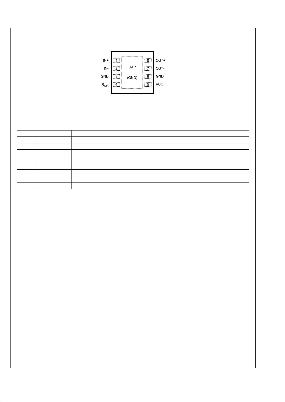
Connection Diagram
20199901
8-Pad LLP
Order Number DS15BA101SD or DS15BA101SDX
See NS Package Number SDA08A
Pin Descriptions
Pin # Name Description
1 IN+ Non-inverting input pin.
2 IN- Inverting input pin.
3 GND Circuit common (ground reference).
4 R
VO
Output voltage amplitude control. Connect a resistor to VCC to set output voltage.
5 V
CC
Positive power supply (+3.3V).
6 GND Circuit common (ground reference).
7 OUT- Non-inverting output pin.
8 OUT+ Inverting output pin.
3 www.national.com
DS15BA101
Page 4

Device Operation
INPUT INTERFACING
The DS15BA101 accepts either differential or single-ended
input. The inputs are self-biased, allowing for simple AC or
DC coupling. DC-coupled inputs must be kept within the spec-
ified common-mode range. The IN+ and IN- pins are selfbiased at approximately 2.1V with VCC = 3.3V. The following
three figures illustrate typical DC-coupled interface to common differential drivers.
20199920
Typical LVDS Driver DC-Coupled Interface to DS15BA101 Input
20199921
Typical CML Driver DC-Coupled Interface to DS15BA101 Input
20199922
Typical LVPECL Driver DC-Coupled Interface to DS15BA101 Input
www.national.com 4
DS15BA101
Page 5

OUTPUT INTERFACING
The DS15BA101 uses current mode outputs. Single-ended
output levels are 400 mV
P-P
into AC-coupled 100Ω differential
cable (with RVO = 953Ω) or into AC-coupled 50Ω coaxial cable
(with RVO = 487Ω). Output level is controlled by the value of
the RVO resistor connected between the RVO and VCC.
The RVO resistor should be placed as close as possible to the
RVO pin. In addition, the copper in the plane layers below the
RVO network should be removed to minimize parasitic capacitance. The following figure illustrates typical DC-coupled interface to common differential receivers and assumes that the
receivers have high impedance inputs. While most receivers
have a common mode input range that can accomodate CML
signals, it is recommended to check respective receiver's
datasheet prior to implementing the suggested interface implementation.
20199923
Typical DS15BA101 Output DC-Coupled Interface to an LVDS, CML or LVPECL Receiver
5 www.national.com
DS15BA101
Page 6

CABLE EXTENDER APPLICATION
The DS15BA101 together with the DS15EA101 form a cable
extender chipset optimized for extending serial data streams
from serializer/deserializer (SerDes) pairs and field programmable gate arrays (FPGAs) over 100Ω differential (i.e.
CAT5e/6/7 and twinax) and 50Ω coaxial cables. Setting correct DS15BA101 output amplitude and proper cable termination are keys for optimal operation. The following two figures
show recommended chipset configuration for 100Ω differen-
tial and 50Ω coaxial cables.
20199905
Cable Extender Chipset Connection Diagram for 100Ω Differential Cables
20199906
Cable Extender Chipset Connection Diagram for 50Ω Coaxial Cables
REFERENCE DESIGN
There is a complete reference design (P/N: DriveCable02EVK) available for evaluation of the cable extender chipset (DS15BA101
and DS15EA101). Fore more information visit http://www.national.com/appinfo/lvds/drivecable02evk.html.
www.national.com 6
DS15BA101
Page 7

Typical Performance
20199910
1.5 Gbps Differential DS15BA101 Output
RVO = 953Ω, H:100 ps / DIV, V:100 mV / DIV
20199912
1.5 Gbps Single-ended DS15BA101 Output
RVO = 487Ω, H:100 ps / DIV, V:100 mV / DIV
20199911
2.0 Gbps Differential DS15BA101 Output
RVO = 953Ω, H:100 ps / DIV, V:100 mV / DIV
20199913
2.0 Gbps Single-ended DS15BA101 Output
RVO = 487Ω, H:100 ps / DIV, V:100 mV / DIV
7 www.national.com
DS15BA101
Page 8

Physical Dimensions inches (millimeters) unless otherwise noted
8-Pad LLP
Order Number DS15BA101SD or DS15BA101SDX
NS Package Number SDA08A
(See AN-1187 for PCB Design and Assembly Recommendations)
www.national.com 8
DS15BA101
Page 9

Notes
9 www.national.com
DS15BA101
Page 10

Notes
DS15BA101 1.5 Gbps Differential Buffer with Adjustable Output Voltage
THE CONTENTS OF THIS DOCUMENT ARE PROVIDED IN CONNECTION WITH NATIONAL SEMICONDUCTOR CORPORATION
(“NATIONAL”) PRODUCTS. NATIONAL MAKES NO REPRESENTATIONS OR WARRANTIES WITH RESPECT TO THE ACCURACY
OR COMPLETENESS OF THE CONTENTS OF THIS PUBLICATION AND RESERVES THE RIGHT TO MAKE CHANGES TO
SPECIFICATIONS AND PRODUCT DESCRIPTIONS AT ANY TIME WITHOUT NOTICE. NO LICENSE, WHETHER EXPRESS,
IMPLIED, ARISING BY ESTOPPEL OR OTHERWISE, TO ANY INTELLECTUAL PROPERTY RIGHTS IS GRANTED BY THIS
DOCUMENT.
TESTING AND OTHER QUALITY CONTROLS ARE USED TO THE EXTENT NATIONAL DEEMS NECESSARY TO SUPPORT
NATIONAL’S PRODUCT WARRANTY. EXCEPT WHERE MANDATED BY GOVERNMENT REQUIREMENTS, TESTING OF ALL
PARAMETERS OF EACH PRODUCT IS NOT NECESSARILY PERFORMED. NATIONAL ASSUMES NO LIABILITY FOR
APPLICATIONS ASSISTANCE OR BUYER PRODUCT DESIGN. BUYERS ARE RESPONSIBLE FOR THEIR PRODUCTS AND
APPLICATIONS USING NATIONAL COMPONENTS. PRIOR TO USING OR DISTRIBUTING ANY PRODUCTS THAT INCLUDE
NATIONAL COMPONENTS, BUYERS SHOULD PROVIDE ADEQUATE DESIGN, TESTING AND OPERATING SAFEGUARDS.
EXCEPT AS PROVIDED IN NATIONAL’S TERMS AND CONDITIONS OF SALE FOR SUCH PRODUCTS, NATIONAL ASSUMES NO
LIABILITY WHATSOEVER, AND NATIONAL DISCLAIMS ANY EXPRESS OR IMPLIED WARRANTY RELATING TO THE SALE
AND/OR USE OF NATIONAL PRODUCTS INCLUDING LIABILITY OR WARRANTIES RELATING TO FITNESS FOR A PARTICULAR
PURPOSE, MERCHANTABILITY, OR INFRINGEMENT OF ANY PATENT, COPYRIGHT OR OTHER INTELLECTUAL PROPERTY
RIGHT.
LIFE SUPPORT POLICY
NATIONAL’S PRODUCTS ARE NOT AUTHORIZED FOR USE AS CRITICAL COMPONENTS IN LIFE SUPPORT DEVICES OR
SYSTEMS WITHOUT THE EXPRESS PRIOR WRITTEN APPROVAL OF THE CHIEF EXECUTIVE OFFICER AND GENERAL
COUNSEL OF NATIONAL SEMICONDUCTOR CORPORATION. As used herein:
Life support devices or systems are devices which (a) are intended for surgical implant into the body, or (b) support or sustain life and
whose failure to perform when properly used in accordance with instructions for use provided in the labeling can be reasonably expected
to result in a significant injury to the user. A critical component is any component in a life support device or system whose failure to perform
can be reasonably expected to cause the failure of the life support device or system or to affect its safety or effectiveness.
National Semiconductor and the National Semiconductor logo are registered trademarks of National Semiconductor Corporation. All other
brand or product names may be trademarks or registered trademarks of their respective holders.
Copyright© 2007 National Semiconductor Corporation
For the most current product information visit us at www.national.com
National Semiconductor
Americas Customer
Support Center
Email:
new.feedback@nsc.com
Tel: 1-800-272-9959
National Semiconductor Europe
Customer Support Center
Fax: +49 (0) 180-530-85-86
Email: europe.support@nsc.com
Deutsch Tel: +49 (0) 69 9508 6208
English Tel: +49 (0) 870 24 0 2171
Français Tel: +33 (0) 1 41 91 8790
National Semiconductor Asia
Pacific Customer Support Center
Email: ap.support@nsc.com
National Semiconductor Japan
Customer Support Center
Fax: 81-3-5639-7507
Email: jpn.feedback@nsc.com
Tel: 81-3-5639-7560
www.national.com
 Loading...