

Page 1
General Description
The DS1372 is a 32-bit binary up counter and 24-bit
down counter with a unique 64-bit ID. The counters, ID,
configuration, and status registers are accessed using
an I2C serial interface. The DS1372 includes a
SQW/INT open-drain output that can output either a
square wave at one of four predefined frequencies, or it
can output an active-low signal when the 24-bit down
counter reaches 0.
Applications
Portable Audio and Video Players
Features
♦ Compliant with Microsoft Windows Media®DRM
10 for Portable Devices
♦ 32-Bit Binary Counter
♦ Programmable Alarm
♦ 64-Bit Factory-Programmed ID
♦ Interrupt Output
♦ I
2
C Serial Interface
♦ Two Selectable I
2
C Addresses
♦ 2.4V to 5.5V Operating Voltage Range
♦ 1.3V to 5.5V Timekeeping Operating Range
♦ -40°C to +85°C Operating Temperature Range
♦ 8-Pin µSOP
DS1372
________________________________________________________________
Maxim Integrated Products
1
μ
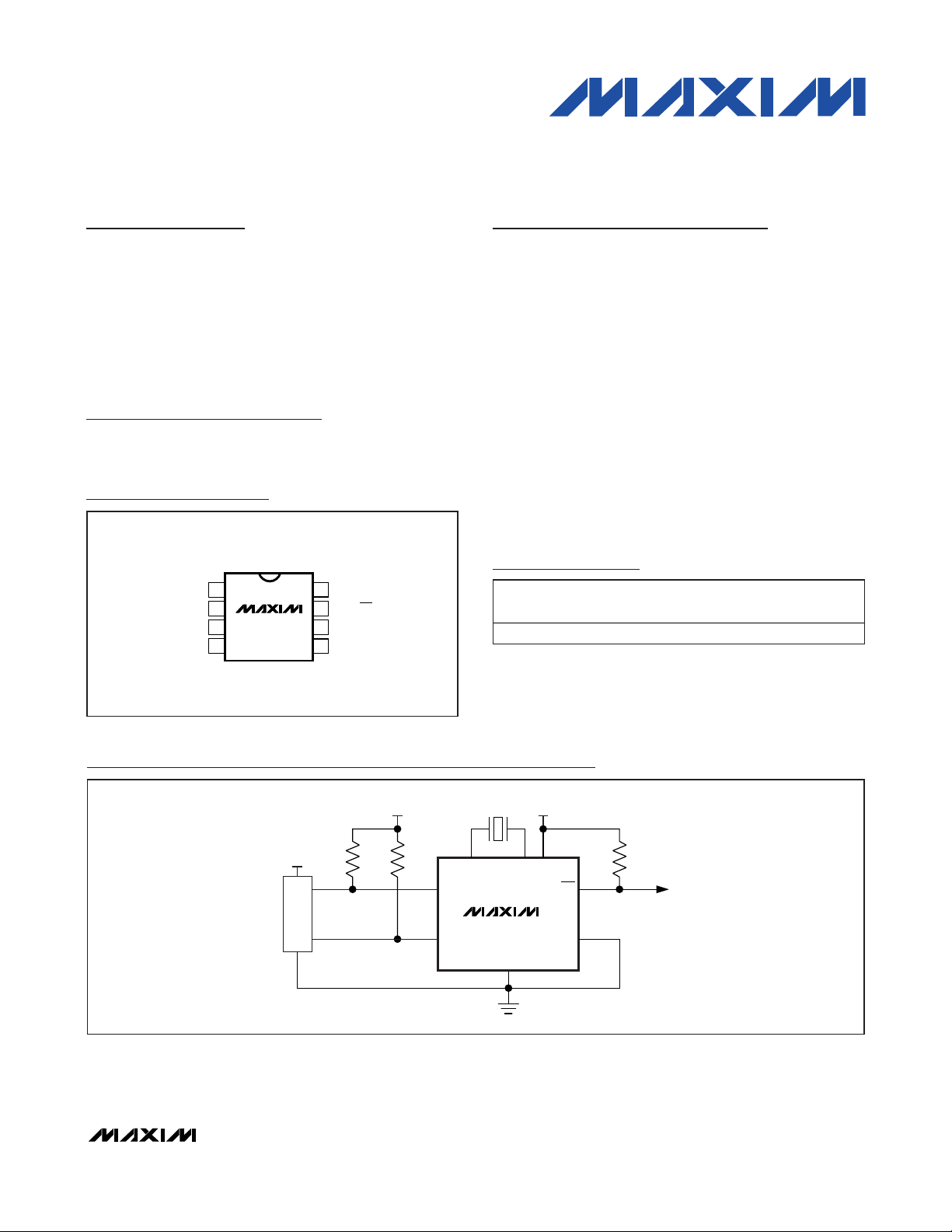
Pin Configuration
Ordering Information
SCL
SDA
SQW/INT
GND
R
PU
RPU = tR / C
B
R
PU
CPU
V
CC
V
CC
X1 X2 V
CC
CRYSTAL
V
CC
DS1372
AD0
Typical Operating Circuit
Rev 0; 7/07
For pricing, delivery, and ordering information, please contact Maxim Direct at 1-888-629-4642,
or visit Maxim’s website at www.maxim-ic.com.
+
Denotes a lead-free package. This symbol also appears on the
top mark.
Windows Media is a registered trademark of Microsoft Corp.
I2C, 32-Bit, Binary Counter Clock with 64-Bit ID
TOP VIEW
AD0
+
X1
1
X2
2
DS1372
3
4
SOP
8
7
6
5
V
CC
SQW/INT
SCL
SDAGND
PART TEMP RANGE PIN-PACKAGE
DS1372U+ -40°C to +85°C 8 μSOP 1372
TOP
MARK
Page 2
DS1372
2 _______________________________________________________________________________________
ABSOLUTE MAXIMUM RATINGS
RECOMMENDED DC ELECTRICAL CHARACTERISTICS
(VCC= 2.4V to 5.5V, TA= -40°C to +85°C, unless otherwise noted.) (Note 1)
Stresses beyond those listed under “Absolute Maximum Ratings” may cause permanent damage to the device. These are stress ratings only, and functional
operation of the device at these or any other conditions beyond those indicated in the operational sections of the specifications is not implied. Exposure to
absolute maximum rating conditions for extended periods may affect device reliability.
Voltage Range on Any Pin Relative to Ground…..-0.3V to +6.0V
Continuous Power Dissipation (T
A
= +70°C)
(derate 4.5mW/°C above +70°C) ……………………. ....360mW
Operating Temperature Range
(noncondensing)……. .......................................-40°C to +85°C
Storage Temperature Range…………………….-55°C to +125°C
Soldering Temperature………….......See IPC/JEDEC J-STD-020
specification.
ELECTRICAL CHARACTERISTICS
(VCC= 2.4V to 5.5V, TA= -40°C to +85°C, unless otherwise noted.) (Note 1)
I2C, 32-Bit, Binary Counter Clock with 64-Bit ID
Supply Voltage V
Active Supply Current I
Standby Current
(Oscillator Enabled)
Data Retention
(Oscil lator Disabled)
Input Logic 1
AD0, SCL, SDA
Input Logic 0
AD0, SCL, SDA
Input Leakage
AD0, SCL, SDA, SQW/INT
Output Logic 0 I
PARAMETER SYMBOL CONDITIONS MIN TYP MAX UNITS
Operating voltage range (Notes 2 and 3) 2.4 5.5
Timekeeping operating range
(Notes 2 and 4)
(Note 3) 35 90 μA
EOSC = 0
(Notes 4 and 5)
EOSC = 1 (Note 4) 25 100 nA
(Note 2)
IH
(Note 2) -0.3
IL
SDA, SQW/INT high impedance -1 +1 μA
VOL = 0.4V (VCC > 2.4V), SDA, SQW/INT 3
VOL = 0.2VCC (1.3V < VCC < 2.4V), SQW/INT 0.250
CCA
I
CCS
I
DDR
V
V
I
OL
CC
LI
1.3 5.5
SQW = 32kHz 600 1300
SQW = 0 400 800
0.7 x
V
CC
VCC +
0.3
0.3 x
V
CC
V
nA
V
V
mA
SCL Clock Frequency (Note 6) f
Bus-Free Time Between a STOP
and START Condition
Hold Time (Repeated) START
Condition (Note 7)
Low Period of SCL Clock t
High Period of SCL Clock t
Setup Time for Repeated START
Condition
Data Hold Time (Notes 8 and 9) t
PARAMETER SYMBOL CONDITIONS MIN TYP MAX UNITS
SCL
t
BUF
t
HD:STA
LOW
HIGH
t
SU:STA
HD:DAT
Fast mode 100 400
Standard mode 0.04 100.00
Fast mode 1.3
Standard mode 4.7
Fast mode 0.6
Standard mode 4.0
Fast mode 1.3
Standard mode 4.7
Fast mode 0.6
Standard mode 4.0
Fast mode 0.6
Standard mode 4.7
Fast mode 0 0.9
Standard mode 0
kHz
μs
μs
μs
μs
μs
μs
Page 3
DS1372
_______________________________________________________________________________________ 3
Note 1: Limits at -40°C are guaranteed by design and not production tested.
Note 2: All voltages are referenced to ground.
Note 3: SCL clocking at maximum frequency = 400kHz.
Note 4: Specified with I
2
C bus inactive, SCL = SDA = VCC.
Note 5: Measured with a 32.768kHz crystal attached to the X1 and X2 pins.
Note 6: The I
2
C minimum operating frequency is imposed by the requirement of timeout period.
Note 7: The first clock pulse is generated after this period.
Note 8: A device must internally provide a hold time of at least 300ns for the SDA signal (referred to as the V
IHMIN
of the SCL sig-
nal) to bridge the undefined region of the falling edge of SCL.
Note 9: The maximum t
HD:DAT
must only be met if the device does not stretch the low period (t
LOW
) of the SCL signal.
Note 10: A fast-mode device can be used in a standard-mode system, but the requirement t
SU:DAT
≥ 250ns must then be met.
This is automatically the case if the device does not stretch the low period of the SCL signal. If such a device does stretch
the low period of the SCL signal, it must output the next data bit to the SDA line t
R(MAX)
+ t
SU:DAT
= 1000 + 250 = 1250ns
before the SCL line is released.
Note 11: C
B
= Total capacitance of one bus line in pF.
Note 12: The parameter t
OSF
is the period of time the oscillator must be stopped for the OSF flag to be set over the voltage range of
2.4V ≤ V
CC
≤ V
CC(MAX)
.
Note 13: The DS1372 can detect any single SCL clock held low longer than T
_TIMEOUT
(MIN). The I2C interface is in reset state and
can receive a new START condition when SCL is held low for at least T
_TIMEOUT
(MAX). Once the part detects this condi-
tion the SDA output is released. The oscillator must be running for this function to work.
ELECTRICAL CHARACTERISTICS (continued)
(VCC= 2.4V to 5.5V, TA= -40°C to +85°C, unless otherwise noted.) (Note 1)
CRYSTAL SPECIFICATIONS
PARAMETER SYMBOL MIN TYP MAX UNITS
Nominal Frequency f
O
32.768 kHz
Capacitive Load C
L
12.5 pF
Equivalent Series Resistance ESR 50 k
I2C, 32-Bit, Binary Counter Clock with 64-Bit ID
Data Setup Time (Note 10) t
Rise Time of SDA and SCL
Signals (Note 11)
Fall Time of SDA and SCL Signals
(Note 11)
Setup Time for STOP Condition t
Capacitive Load for Each Bus
Line (Note 11)
I/O Capacitance C
SCL Spike Suppresion TSP 30 ns
Oscillator Stop Flag (OSF) Delay
(Note 12)
Timeout Interval (Note 13) T
PARAMETER SYMBOL CONDITIONS MIN TYP MAX UNITS
SU:DAT
t
R
t
SU:STO
C
I/O
t
OSF
_TIMEOUT
Fast mode 100
Standard mode 250
Fast mode
Standard mode
Fast mode
F
Standard mode
20 +
0.1C
20 +
0.1C
20 +
0.1C
20 +
0.1C
300
B
1000
B
300
B
300
B
Fast mode 0.6
Standard mode 4.0
400 pF
B
10 pF
100 ms
25 35 ms
ns
ns
ns
μs
Page 4
DS1372
4 _______________________________________________________________________________________
Pin Description
Figure 1. Block Diagram
I2C, 32-Bit, Binary Counter Clock with 64-Bit ID
PIN NAME FUNCTION
Connections for Standard 32.768kHz Quartz Crystal. The internal oscillator circuitry is designed for
1, 2 X1, X2
3 AD0
4 GND Ground
5 SDA
6 SCL
7 SQW/INT
8 VCC DC Power Pin. This pin should be decoupled using a 0.1μF or 1.0μF capacitor.
operation with a crystal having a 12.5pF specified load capacitance (C
oscillator and can optionally be connected to an external 32.768kHz oscillator. The output of the
internal oscillator, pin X2, is floated if an external oscillator is connected to pin X1.
Slave Address Input. This pin is the slave address input for the I
access multiple devices on the same bus. To select the device, the address value on the pin
must match the corresponding bit in the device addresses. This pin can be connected to V
ground or be driven to a log ic-high or logic-low leve l.
Serial Data Input/Output. This pin is the data input/output for the I
open drain and requires an external pullup resistor.
Serial Clock Input. This pin is the clock input for the I
2
C serial interface and is used to synchronize
data movement on the serial interface.
Square Wave or Active-Low Interrupt Open-Drain Output. This pin is used to output the square wave
or alarm interrupt signal. The function of this pin is selected by the state of the INTCN control bit.
Thi s pin is open drain and requires an e xternal pul lup resistor.
). Pin X1 is the input to the
L
2
C serial interface and is used to
2
C serial interface. The SDA pin is
CC
or
X1
V
GND
SDA
SCL
AD0
X2
CC
OSCILLATOR
POWER
I2C
INTERFACE
÷4
CONTROL/
64-BIT ID
STATUS
ROM
RS[2:1]
32,768HzDIVIDER CHAIN
8192Hz
4096Hz
÷2
÷4096
÷4096
1Hz
1Hz
CLR
SQW
MUX
32-BIT
COUNTER
24-BIT ALARM
COUNTER
ACE
AF
MUX
INTCN
DS1372
SQW/INT
N
Page 5

Detailed Description
The DS1372 is a 32-bit binary counter designed to continuously count time in seconds. An additional counter
is provided that can generate a periodic alarm. An
interrupt output can be driven when the alarm condition
is met. The device includes a unique, factory-lasered
64-bit ROM ID. The device is programmed serially by
an I2C bidirectional bus.
Oscillator Circuit
The DS1372 is designed to operate with a standard
32.768kHz quartz crystal having a 12.5pF specified
load capacitance (C
L
). For more information on crystal
selection and crystal layout considerations, refer to
Application Note 58:
Crystal Considerations with Dallas
Real-Time Clocks (RTCs)
. An external 32.768kHz oscillator can be used as the DS1372’s time base. In this
configuration, the X1 pin is connected to the external
oscillator signal and the X2 is floated. The EOSC bit in
the Control Register controls oscillator operation.
Clock Accuracy
The initial clock accuracy is dependent upon the accuracy of the crystal and the accuracy of the match
between the capacitive load of the oscillator circuit and
the capacitive load for which the crystal was trimmed.
Additional error is added by crystal frequency drift
caused by temperature shifts. External circuit noise coupled into the oscillator circuit can result in the clock running fast. Figure 2 shows a typical PCB layout for
isolation of the crystal and oscillator from noise. Refer to
Application Note 58:
Crystal Considerations with Dallas
Real-Time Clocks (RTCs)
for detailed information.
Operation
The block diagram in Figure 1 shows the DS1372’s main
elements. As shown, communications to and from the
DS1372 occur serially over an I
2
C bidirectional bus. The
DS1372 operates as a slave device on the serial bus.
Access is obtained by implementing a START condition
and providing a device identification code followed by a
register address. Subsequent registers can be accessed
sequentially until a STOP condition is executed.
Address Map
Table 1 shows the address map for the DS1372 registers. During a multibyte access, when the address
pointer reaches the end of the register space (10h) it
wraps around to location 00h. On an I2C START or
address pointer incrementing to location 00h, the current time is transferred to a second set of registers. The
time information is read from these secondary registers,
while the clock may continue to run. This eliminates the
need to reread the registers in case the main registers
update during a read.
Clock Operation
The clock counter is a 32-bit up counter. The counter
counts up once per second. The contents can be read
or written by accessing the address range 00h–03h. On
an I2C START, or when the address pointer rolls over to
00h, the current value is latched into a register, which is
output on the serial data line while the counter continues to increment. When writing to the registers, the
divider chain is reset when register 00h is written. Once
the divider chain is reset, the remaining clock registers
should be written within one second to avoid rollover
issues. Additionally, to avoid rollover issues the clock
registers must also be written from LSB to MSB, and all
four bytes should always be written.
DS1372
_______________________________________________________________________________________ 5
Figure 2. Layout Example
I2C, 32-Bit, Binary Counter Clock with 64-Bit ID
CRYSTAL
LOCAL GROUND PLANE (LAYER 2)
X1
X2
Page 6

DS1372
Alarm Operation
The alarm counter is a 24-bit counter in the address
range 04h–06h. When the alarm counter is written, a
seed register is written with the alarm counter value.
When the alarm counter enable (ACE) bit in the Control
Register is set to 1, the counter begins counting down
from the seed value. When the counter reaches zero, it
sets the AF bit in the Status Register, if the AF bit is not
already set. If the AIE and INTCN bits are both set to a
logic 1, the SQW/INT pin goes low and remains low
until AF is written to logic 0. The counter is then
reloaded with the seed value and the countdown
restarts. When the counter is read, the current counter
value is latched into a register, which is output on the
serial data line while the counter continues to decrement. The counter is disabled if the seed value is zero
or if ACE = 0. Whenever the ACE is set from 0 to 1, the
counter is reloaded with the current seed value and the
counter begins to count down. Note: When initializing
or changing the alarm value, the ACE bit should be
enabled after writing the alarm counter bytes.
6 _______________________________________________________________________________________
Table 1. DS1372 Address Map
Note: Unless otherwise specified, the states of the registers are undefined when power is first applied. Bits shown as 0 always read
back as 0.
I2C, 32-Bit, Binary Counter Clock with 64-Bit ID
ADDRESS REGISTER BIT 7 BIT 6 BIT 5 BIT 4 BIT 3 BIT 2 BIT 1 BIT 0
00h Cloc k — Seconds Counter Byte 0 LSB
01h Cloc k — Seconds Counter B yte 1 —
02h Cloc k — Seconds Counter B yte 2 —
03h Cloc k MSB Seconds Counter Byte 3 —
04h Alarm — Alarm Counter Byte 0 LSB
05h Alarm — Alarm Counter Byte 1 —
06h Alarm MSB A larm Counter Byte 2 —
07h Control EOSC ACE 0 0 INTCN RS2 RS1 AIE
08h Status OSF 0 0 0 0 0 0 AF
09h ID Model Number
0Ah ID Serial Number Byte 0
0Bh ID Serial Number Byte 1
0Ch ID Serial Number Byte 2
0Dh ID Serial Number Byte 3
0Eh ID Serial Number Byte 4
0Fh ID Serial Number Byte 5
10h ID CRC
Page 7

Control Register (07h)
Bit 7: Enable Oscillator (EOSC). When set to logic 0,
the oscillator is started. When set to logic 1, the oscillator is stopped. This bit is clear (logic 0) when power is
first applied.
Bit 6: Alarm Counter Enable (ACE). When set to logic
1, the alarm counter is enabled. If alarm counter seed
register has a nonzero value, the counter runs and sets
the AF bit to 1 when the counter reaches 0. When set to
logic 0, the alarm counter is disabled, and the counter
can be used as RAM. This bit is clear (logic 0) when
power is first applied.
Bit 3: Interrupt Control (INTCN). This bit controls the
SQW/INT signal. When the INTCN bit is set to logic 0, a
square wave is output on the SQW/INT pin whose frequency is defined by bits RS2 and RS1, according to
Table 2. The oscillator must also be enabled for the
square wave to be output. When the INTCN bit is set to
logic 1, this permits the AF bit in the Status Register to
assert SQW/INT (provided that ACE and AIE are also
enabled) whenever AF = 1. If ACE = 1, the alarm flag is
always set on an alarm condition, regardless of the
state of the INTCN bit. The INTCN bit is set to logic 1
when power is first applied.
Bits 2 and 1: Rate Select (RS[2:1]). These bits control
the frequency of the square-wave output when the
square wave has been enabled. Table 2 shows the
square-wave frequencies that can be selected with the
RS bits. These bits are both set (logic 1) when power is
first applied.
Bit 0: Alarm Interrupt Enable (AIE). When set to a
logic 1, this bit permits the alarm flag (AF) to assert
SQW/INT (when INTCN = 1). The AIE bit is disabled
(logic 0) when power is first applied.
Table 2. Square-Wave/Interrupt Output
Frequencies
Note: When interrupt operation is enabled, the SQW/INT out-
put is the inverse of the AF bit.
Control Register (07h)
DS1372
_______________________________________________________________________________________ 7
Special Purpose Registers
The DS1372 has two additional registers that control
the alarm counter and interrupts: Control Register (07h)
and Status Register (08h).
I2C, 32-Bit, Binary Counter Clock with 64-Bit ID
Bit # 7 6 5 4 3 2 1 0
Name EO SC ACE 0 0 INTCN RS2 RS1 AIE
Reset 0 0 0 0 1 1 1 0
INTCN ACE AIE R S2 RS1
0 X X 0 0 1Hz
0 X X 0 1 4.096kHz
0 X X 1 0 8.192kHz
0 X X 1 1 32.768kHz
1 1 1 X X Interrupt
SQW/INT
OUTPUT
Page 8

DS1372
Status Register (08h)
Bit 7: Oscillator Stop Flag (OSF). A logic 1 in this bit
indicates that the oscillator either is stopped or was
stopped for some period of time and may be used to
judge the validity of the timekeeping data. This bit is set
to logic 1 anytime the oscillator stops. The following are
examples of conditions that can cause the OSF bit to
be set:
1) The first time power is applied.
2) The voltage present on VCCis insufficient to support oscillation.
3) The EOSC bit is turned off.
4) External influences on the crystal (i.e., noise, leakage, etc.) exist.
This bit remains at logic 1 until written to logic 0.
Bits 6 to 1: These bits always read back as logic 0.
Bit 0: Alarm Flag (AF). A logic 1 in the AF bit indicates
that the alarm counter reached zero. If the AIE and
INTCN bits are both set to logic 1, the SQW/INT pin
goes low and remains low until AF is written to logic 0.
This bit can only be written to logic 0. Attempting to
write logic 1 leaves the value unchanged.
ID Register
A unique 64-bit lasered serial number is located in the
address range 09h–10h. This serial number is divided
into three parts. The first byte in register 09h contains a
model number to identify the DS1372 device type.
Registers 0Ah–0Fh contain a unique binary number.
Register 10h contains a CRC byte used to validate the
data in registers 09h–0Fh. All eight bytes of the serial
number are read-only registers. The CRC byte is generated with the polynomial equal to x8+ x5+ x4+ 1 (see
Figure 3).
The DS1372 is manufactured such that no two devices
contain an identical number in locations 0Ah–0Fh.
I2C Serial Data Bus
The DS1372 supports a bidirectional I2C serial bus and
data transmission protocol (Figure 4). A device that
sends data onto the bus is defined as a transmitter,
and a device receiving data is defined as a receiver.
The device that controls the message is called a master. The devices that are controlled by the master are
slaves. The bus must be controlled by a master device
that generates the serial clock (SCL), controls the
bus access, and generates the START and STOP
8 _______________________________________________________________________________________
Status Register (08h)
Figure 3. CRC Byte Polynomial
I2C, 32-Bit, Binary Counter Clock with 64-Bit ID
Bit # 7 6 5 4 3 2 1 0
Name OSF 0 0 0 0 0 0 AF
Reset 1 0 0 0 0 0 0 0
POLYNOMIAL = X8 + X5 + X4 + 1
1ST
STAGE
0
X
2ND
STAGE
X
3RD
STAGE
1
2
X
4TH
STAGE
3
X
5TH
STAGE
4
X
5
X
6TH
STAGE
X
6
7TH
STAGE
7
X
8TH
STAGE
8
X
INPUT DATA
Page 9

conditions. The DS1372 operates as a slave on the I2C
bus. Connections to the bus are made through the SCL
input and open-drain SDA I/O lines. Within the bus
specifications, a standard mode (100kHz maximum
clock rate) and a fast mode (400kHz maximum clock
rate) are defined. The DS1372 works in both modes.
The following bus protocol has been defined (Figure 5):
• Data transfer can be initiated only when the bus is
not busy.
• During data transfer, the data line must remain stable
whenever the clock line is high. Changes in the data
line while the clock line is high are interpreted as
control signals.
DS1372
_______________________________________________________________________________________ 9
Figure 4. Data Transfer on I2C Serial Bus
Figure 5. I2C Data Transfer Overview
I2C, 32-Bit, Binary Counter Clock with 64-Bit ID
SDA
t
BUF
t
LOW
SCL
t
HD:STA
STOP START
SDA
MSB
SLAVE ADDRESS
t
R
t
HD:DAT
t
F
t
HIGH
R/W
DIRECTION
BIT
ACKNOWLEDGEMENT
SIGNAL FROM RECEIVER
t
SU:DAT
REPEATED
START
t
SU:STA
t
HD:STA
ACKNOWLEDGEMENT
SIGNAL FROM RECEIVER
t
SP
t
SU:STO
SCL
12 678 9 12 893–7
START
CONDITION
ACK
REPEATED IF MORE BYTES
ARE TRANSFERED
ACK
STOP
CONDITION
OR REPEATED
START
CONDITION
Page 10

DS1372
Accordingly, the following bus conditions have been
defined:
Bus not busy: Both data and clock lines remain
high.
Start data transfer: A change in the state of the
data line from high to low, while the clock line is high,
defines a START condition.
Stop data transfer: A change in the state of the data
line from low to high, while the clock line is high,
defines a STOP condition.
Data valid: The state of the data line represents
valid data when, after a START condition, the data
line is stable for the duration of the high period of the
clock signal. The data on the line must be changed
during the low period of the clock signal. There is
one clock pulse per bit of data.
Each data transfer is initiated with a START condition
and terminated with a STOP condition. The number
of data bytes transferred between the START and
the STOP conditions is not limited, and is determined
by the master device. The information is transferred
byte-wise and each receiver acknowledges with a
ninth bit.
Acknowledge: Each receiving device, when
addressed, is obliged to generate an acknowledge
after the reception of each byte. The master device
must generate an extra clock pulse, which is associated with this acknowledge bit.
A device that acknowledges must pull down the SDA
line during the acknowledge clock pulse in such a
way that the SDA line is stable low during the high
period of the acknowledge-related clock pulse. Of
course, setup and hold times must be taken into
account. A master must signal an end of data to the
slave by not generating an acknowledge bit on the
last byte that has been clocked out of the slave. In
this case, the slave must leave the data line high to
enable the master to generate the STOP condition.
Timeout: To avoid an unintended I2C interface time-
out, SCL should not be held low longer than 25ms.
The I2C interface is in the reset state and can
receive a new START condition when SCL is held
low for at least 35ms. When the part detects this condition, SDA is released and allowed to float. For the
timeout function to work, the oscillator must be
enabled and running.
Depending upon the state of the R/W bit, two types of
data transfer are possible:
1) Data transfer from a master transmitter to a
slave receiver. The first byte transmitted by the
master is the slave address. Next follows a number of data bytes. The slave returns an acknowledge bit after each received byte. Data is
transferred with the most significant bit (MSB) first.
2) Data transfer from a slave transmitter to a
master receiver. The first byte (the slave
address) is transmitted by the master. The slave
then returns an acknowledge bit. Next follows a
number of data bytes transmitted by the slave to
the master. The master returns an acknowledge
bit after all received bytes other than the last byte.
At the end of the last received byte, a not
acknowledge is returned.
The master device generates all the serial clock
pulses and the START and STOP conditions. A
transfer is ended with a STOP condition or with a
repeated START condition. Since a repeated
START condition is also the beginning of the next
serial transfer, the bus will not be released. Data
is transferred with the most significant bit (MSB)
first.
The DS1372 can operate in the following two modes:
1) Slave receiver mode (DS1372 write mode): Serial
data and clock are received through SDA and SCL.
After each byte is received an acknowledge bit is
transmitted. START and STOP conditions are recognized as the beginning and end of a serial transfer.
Address recognition is performed by hardware after
reception of the slave address and direction bit (see
Figure 6). The slave address byte is the first byte
received after the master generates the START condition. The slave address byte contains the 7-bit
DS1372 address, which is 110100 and AD0. Each
slave address is followed by the direction bit (R/W),
which is zero for a write. The bit position signified by
A is compared to the value on the AD0 input pin.
After receiving and decoding the slave address
byte, the device outputs an acknowledge on the
SDA line. After the device acknowledges the slave
address and write bit, the master transmits a register
address to the device. This sets the register pointer
on the device. After setting the register address, the
master then transmits each byte of data with the
DS1372 acknowledging each byte received. The
master generates a STOP condition to terminate the
data write.
10 ______________________________________________________________________________________
I2C, 32-Bit, Binary Counter Clock with 64-Bit ID
Page 11

2) Slave transmitter mode (DS1372 read mode): The
first byte is received and handled as in the slave
receiver mode. However, in this mode, the direction
bit indicates that the transfer direction is reversed.
The DS1372 transmits serial data on SDA while the
serial clock is input on SCL. START and STOP conditions are recognized as the beginning and end of
a serial transfer (see Figure 7). The slave address
byte is the first byte received after the master generates the START condition. The slave address byte
contains the 7-bit DS1372 address, which is 110100
and AD0. Each slave address is followed by the
direction bit (R/W), which is one for a read. The bit
position signified by A is compared to the value on
the AD0 pin. After receiving and decoding the slave
address byte, the device outputs an acknowledge
on the SDA line. The DS1372 then begins to transmit
data starting with the register address pointed to by
the register pointer. If the register pointer is not written to before the initiation of a read mode, the first
address that is read is the last one stored in the register pointer. The DS1372 must receive a "not
acknowledge" to end a read.
DS1372
______________________________________________________________________________________ 11
Figure 6. Data Write—Slave Receiver Mode
Figure 7. Data Read (from Current Pointer Location)—Slave Transmitter Mode
Figure 8. Data Read (Write Pointer, Then Read)—Slave Receive and Transmit
I2C, 32-Bit, Binary Counter Clock with 64-Bit ID
<SLAVE ADDRESS> <R/W> <WORD ADDRESS (n)> <DATA (n)> <DATA (n + 1)> <DATA (n + X)
AXXXXXXXXA110100S AD0 0 XXXXXXXX A XXXXXXXX A XXXXXXXX A P
S - START
A - ACKNOWLEDGE (ACK)
P - STOP
R/W - READ/WRITE OR DIRECTION BIT ADDRESS
<SLAVE ADDRESS> <R/W> <DATA (n)> <DATA (n + 1)> <DATA (n + 2)> <DATA (n + X)>
AD0
AXXXXXXXXA110100S 1 XXXXXXXX A XXXXXXXX A XXXXXXXX A P
...
MASTER TO SLAVESLAVE TO MASTER
DATA TRANSFERRED
(X + 1 BYTES + ACKNOWLEDGE)
...
S - START
A - ACKNOWLEDGE (ACK)
P - STOP
A - NOT ACKNOWLEDGE (NACK)
R/W - READ/WRITE OR DIRECTION BIT ADDRESS
MASTER TO SLAVE SLAVE TO MASTER
NOTE: LAST DATA BYTE IS FOLLOWED BY A NACK.
AD0 AXXXXXXXXA110100A 110100AS Sr0 AD0 A1
<DATA (n)> <DATA (n + 1)> <DATA (n + 2)> <DATA (n + X)>
AXXXXXXXX XXXXXXXX A XXXXXXXX A XXXXXXXX A P
S - START
Sr - REPEATED START
A - ACKNOWLEDGE (ACK)
P - STOP
A - NOT ACKNOWLEDGE (NACK)
R/W - READ/WRITE OR DIRECTION BIT ADDRESS
MASTER TO SLAVE SLAVE TO MASTER
DATA TRANSFERRED
(X + 1 BYTES + ACKNOWLEDGE)
<R/W><R/W> <WORD ADDRESS (n)> <SLAVE ADDRESS (n)><SLAVE ADDRESS>
...
DATA TRANSFERRED
(X + 1 BYTES + ACKNOWLEDGE)
NOTE: LAST DATA BYTE IS FOLLOWED BY A NACK.
Page 12

DS1372
Maxim cannot assume responsibility for use of any circuitry other than circuitry entirely embodied in a Maxim product. No circuit patent licenses are
implied. Maxim reserves the right to change the circuitry and specifications without notice at any time.
12
____________________Maxim Integrated Products, 120 San Gabriel Drive, Sunnyvale, CA 94086 408-737-7600
© 2007 Maxim Integrated Products is a registered trademark of Maxim Integrated Products, Inc.
Chip Information
SUBSTRATE CONNECTED TO GROUND
PROCESS: CMOS
Thermal Information
Thermal Resistance (Junction to Ambient) θJA: 221°C/W
Thermal Resistance (Junction to Case) θ
JC
: 39°C/W
Package Information
For the latest package outline information, go to
www.maxim-ic.com/packages.
I2C, 32-Bit, Binary Counter Clock with 64-Bit ID
PACKAGE DOCUMENT NO.
8-pin μSOP 21-0036
 Loading...