

Page 1
1 of 12 111999
FEATURES
Converts CMOS SRAM into nonvolatile
memory
Unconditionally write-protects SRAM when
VCC is out of tolerance
Automatically switches to battery backup
supply when VCC power failure occurs
Flexible memory organization
- Mode 0: 4 banks with 1 SRAM each
- Mode 1: 2 banks with 2 SRAMs each
- Mode 2: 1 bank with 4 SRAMs each
Monitors voltage of a lithium cell and
provides advanced warning of impending
battery failure
Signals low-battery condition on active low
Battery Warning output signal
Resets processor when power failure occurs
and holds processor in reset during system
power-up
Optional -5% or -10% power-fail detection
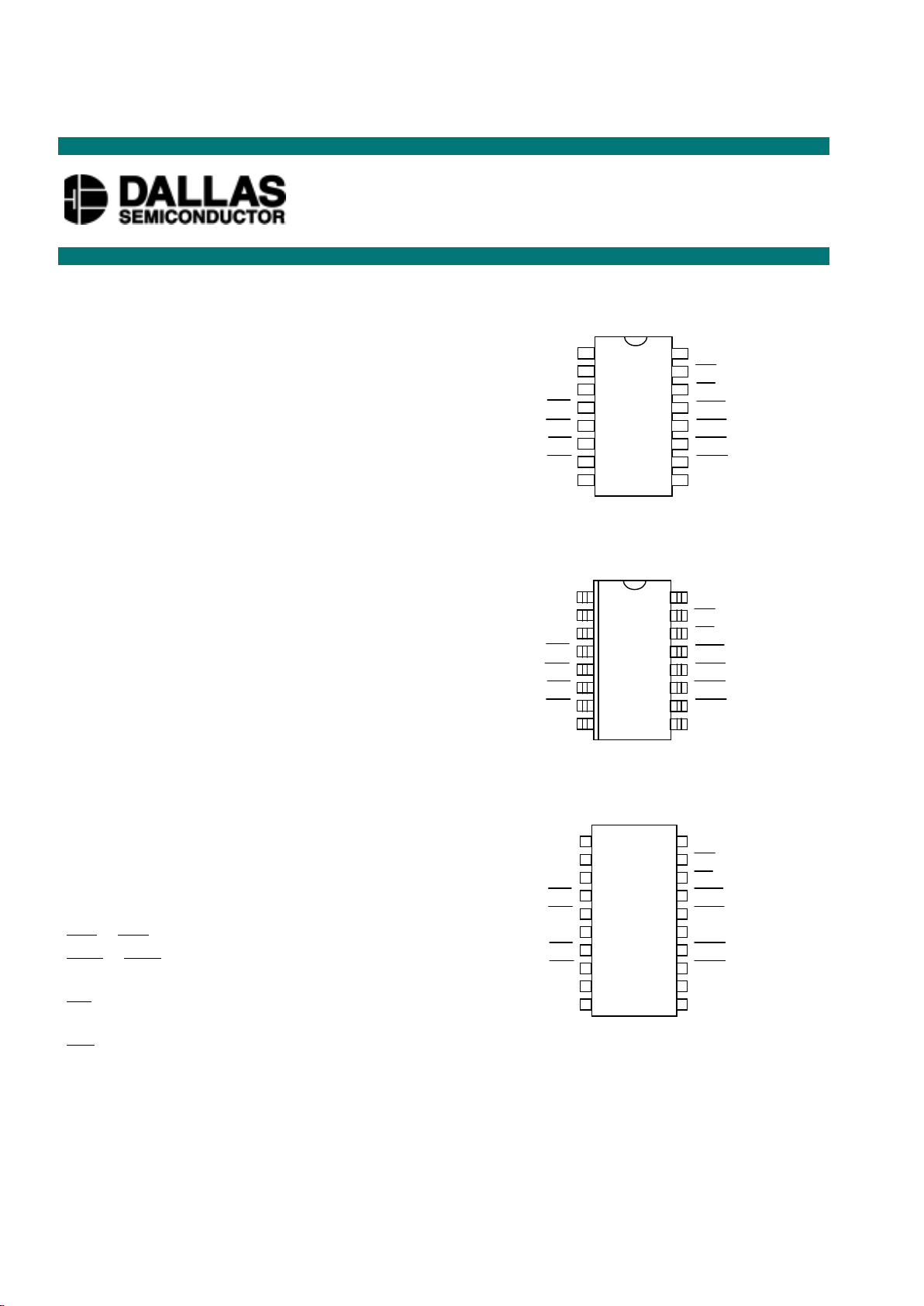
16-pin DIP, 16-pin SOIC and 20-pin TSSOP
packages
Industrial temperature range of -40°C to
+85°C
PIN DESCRIPTION
V
CCI
- +5V Power Supply Input
V
CCO
- SRAM Power Supply Output
V
BAT
- Backup Battery Input
A, B - Address Inputs
CEI1 - CEI4 - Chip Enable Inputs
CEO1 - CEO4 - Chip Enable Outputs
TOL - V
CC
Tolerance Select
BW - Battery Warning Output (Open
Drain)
RST - Reset Output (Open Drain)
MODE - Mode Input
GND - Ground
NC - No Connection
PIN ASSIGNMENT
DS1321
Flexible Nonvolatile Controller with
Lithium Battery Monitor
www.dalsemi.com
1
2
3
4
20
19
18
17
5
6
7
8
9
10 11
12
13
14
15
16
NC
DS1321E 20-Pin TSSOP
V
CCI
RST
BW
CEO1
CEO2
NC
CEO3
CEO4
NC
MODE
V
CCO
V
BAT
TOL
CEI1
CEI2
NC
A
/CEI3
B/CEI4
GND
1
2
3
4
16
15
14
13
5
6
7
89
10
11
12
V
CCI
RST
BW
CEO1
CEO2
CEO3
CEO4
MODE
V
CCO
V
BAT
TOL
CEI1
CEI2
A
/CEI3
B/CEI4
GND
DS1321 16-Pin DIP
(300-mil)
1
2
3
4
16
15
14
13
5
6
7
89
10
11
12
V
CCI
RST
BW
CEO1
CEO2
CEO3
CEO4
MODE
V
CCO
V
BAT
TOL
CEI1
CEI2
A
/CEI3
B/CEI4
GND
DS1321S 16-Pin SOIC
(150-mil)
Page 2

DS1321
2 of 12
DESCRIPTION
The DS1321 Flexible Nonvolatile Controller with Lithium Battery Monitor is a CMOS circuit which
solves the application problem of converting CMOS SRAMs into nonvolatile memory. Incoming power
is monitored for an out-of-tolerance condition. When such a condition is detected, chip enable outputs are
inhibited to accomplish write protection and the battery is switched on to supply the SRAMs with
uninterrupted power. Special circuitry uses a low-leakage CMOS process which affords precise voltage
detection at extremely low battery consumption. One DS1321 can support as many as four SRAMs
arranged in any of three memory configurations.
In addition to battery-backup support, the DS1321 performs the important function of monitoring the
remaining capacity of the lithium battery and providing a warning before the battery reaches end-of-life.
Because the open-circuit voltage of a lithium backup battery remains relatively constant over the majority
of its life, accurate battery monitoring requires loaded-battery voltage measurement. The DS1321
performs such measurement by periodically comparing the voltage of the battery as it supports an internal
resistive load with a carefully selected reference voltage. If the battery voltage falls below the reference
voltage under such conditions, the battery will soon reach end-of-life. As a result, the Battery Warning
pin is activated to signal the need for battery replacement.
MEMORY BACKUP
The DS1321 performs all the circuit functions required to provide battery-backup for as many as four
SRAMs. First, the device provides a switch to direct power from the battery or the system power supply
(V
CCI
). Whenever V
CCI
is less than the V
CCTP
trip point and V
CCI
is less than the battery voltage V
BAT
, the
battery is switched in to provide backup power to the SRAM. This switch has voltage drop of less than
0.2 volts.
Second, the DS1321 handles power failure detection and SRAM write-protection. V
CCI
is constantly
monitored, and when the supply goes out of tolerance, a precision comparator detects power failure and
inhibits the four chip enable outputs in order to write-protect the SRAMs. This is accomplished by
holding CEO1 through CEO4 to within 0.2 volts of V
CCO
when V
CCI
is out of tolerance. If any CEI is
active (low) at the time that power failure is detected, the corresponding CEO signal is kept low until the
CEI signal is brought high again. Once the CEI signal is brought high, the CEO signal is taken high and
held high until after V
CCI
has returned to its nominal voltage level. If the CEI signal is not brought high
by 1.5 µs after power failure is detected, the corresponding CEO is forced high at that time. This specific
scheme for delaying write protection for up to 1.5 µs guarantees that any memory access in progress
when power failure occurs will complete properly. Power failure detection occurs in the range of 4.75 to
4.5 volts (5% tolerance) when the TOL pin is wired to GND or in the range of 4.5 to 4.25 volts (10%
tolerance) when TOL is connected to V
CCO
.
Page 3
DS1321
3 of 12
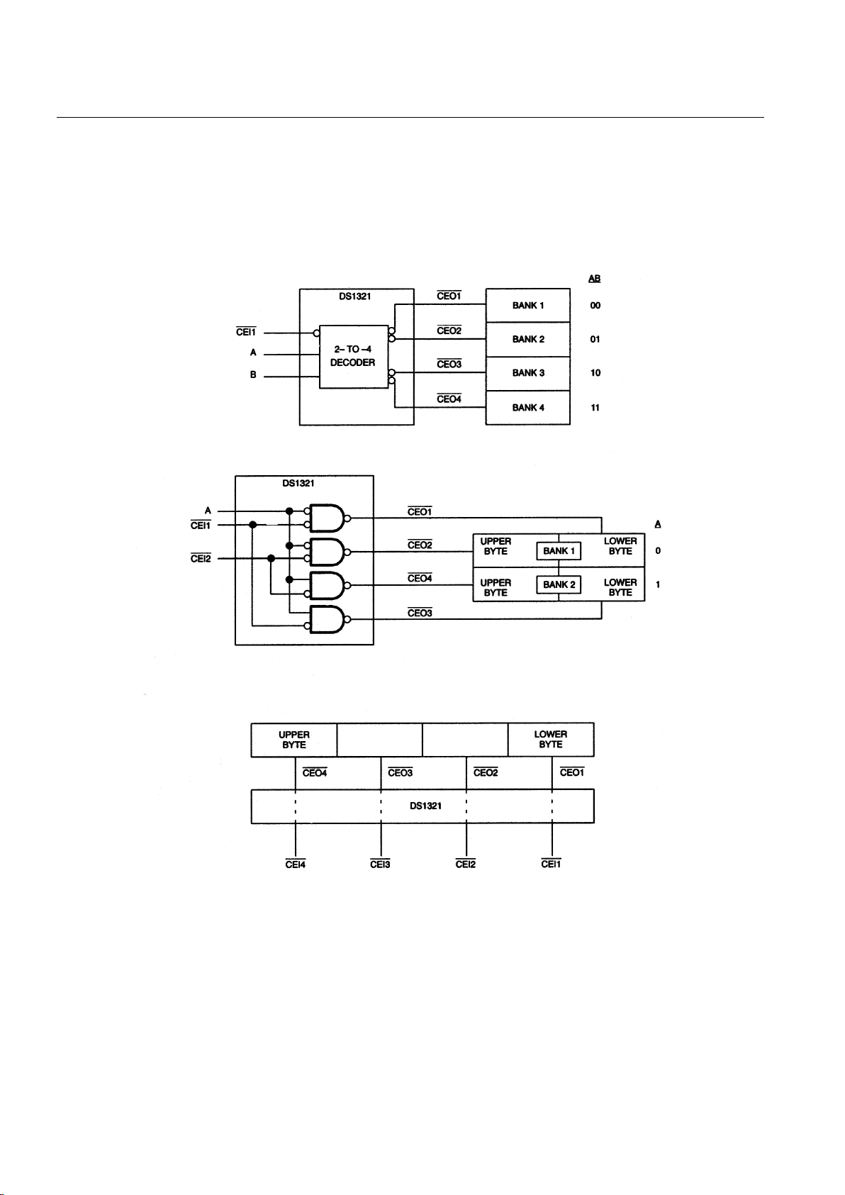
MEMORY CONFIGURATIONS
The DS1321 can be configured via the MODE pin for three different arrangements of the four attached
SRAMs. The state of the MODE pin is latched at V
CCI
= V
CCTP
on power up. See Figure 1 for details.
MEMORY CONFIGURATIONS Figure 1
MODE = GND (4 BANKS WITH 1 SRAM EACH):
MODE = V
CCO
(2 BANKS WITH 2 SRAM EACH):
MODE FLOATING (1 BANK WITH 4 SRAMs):
Page 4

DS1321
4 of 12
BATTERY VOLTAGE MONITORING
The DS1321 automatically performs periodic battery voltage monitoring at a factory-programmed time
interval of 24 hours. Such monitoring begins within t
REC
after V
CCI
rises above V
CCTP
and is suspended
when power failure occurs.
After each 24-hour period (t
BTCN
) has elapsed, the DS1321 connects V
BAT
to an internal 1 MΩ=test
resistor (R
INT
) for one second (t
BTPW
). During this one second, if V
BAT
falls below the factory-
programmed battery voltage trip point (V
BTP
), the battery warning output BW is asserted. While BW is
active, battery testing will be performed with period t
BTCW
to detect battery removal and replacement.
Once asserted, BW remains active until the battery is physically removed and replaced by a fresh cell.
The battery is still retested after each VCC power-up, however, even if BW was active on power-down. If
the battery is found to be higher than V
BTP
during such testing, BW is deasserted and regular 24-hour
testing resumes. BW has an open-drain output driver.
Battery replacement following BW activation is normally done with V
CCI
nominal so that SRAM data is
not lost. During battery replacement, the minimum time duration between old battery detachment and
new battery attachment (t
BDBA
) must be met or BW will not deactivate following attachment of the new
battery. Should BW not deactivate for this reason, the new battery can be detached for t
BDBA
and then re-
attached to clear BW .
NOTE: The DS1321 cannot constantly monitor an attached battery because such monitoring would
drastically reduce the life of the battery. As a result, the DS1321 only tests the battery for one second out
of every 24 hours and does not monitor the battery in any way between tests. If a good battery (one that
has not been previously flagged with BW ) is removed between battery tests, the DS1321 may not
immediately sense the removal and may not activate BW until the next scheduled battery test. If a battery
is then reattached to the DS1321, the battery may not be tested until the next scheduled test.
NOTE: Battery monitoring is only a useful technique when testing can be done regularly over the entire
life of a lithium battery. Because the DS1321 only performs battery monitoring when V
CC
is nominal,
systems which are powered-down for excessively long periods can completely drain their lithium cells
without receiving any advanced warning. To prevent such an occurrence, systems using the DS1321
battery monitoring feature should be powered-up periodically (at least once every few months) in order to
perform battery testing. Furthermore, anytime
BW is activated on the first battery test after a power-up,
data integrity should be checked via checksum or other technique.
POWER MONITORING
The DS1321 automatically detects out-of-tolerance power supply conditions and warns a processor-based
system of impending power failure. When V
CCI
falls below the trip point level defined by the TOL pin
(V
CCTP
), the V
CCI
comparator activates the reset signal RST . Reset occurs in the range of 4.75 to 4.5 volts
(5% tolerance) when the TOL pin is connected to GND or in the range of 4.5 to 4.25 volts (10%
tolerance) when TOL is connected to V
CCO
.
RST also serves as a power-on reset during power-up. After V
CCI
exceeds V
CCTP
, RST will be held active
for 200 ms nominal (t
RPU
). This reset period is sufficiently long to prevent system operation during
power-on transients and to allow t
REC
to expire. RST has an open-drain output driver.
Page 5

DS1321
5 of 12
FRESHNESS SEAL MODE
When the battery is first attached to the DS1321 without V
CC
power applied, the device does not
immediately provide battery-backup power on V
CCO
. Only after V
CCI
exceeds V
CCTP
and later falls below
both V
CCTP
and V
BAT
will the DS1321 leave Freshness Seal Mode and provide battery-backup power.
This mode allows a battery to be attached during manufacturing but not used until after the system has
been activated for the first time. As a result, no battery energy is drained during storage and shipping.
FUNCTIONAL BLOCK DIAGRAM Figure 2
Page 6

DS1321
6 of 12
ABSOLUTE MAXIMUM RATINGS*
Voltage on Any Pin Relative to Ground -0.5V to +7.0V
Operating Temperature -40°C to +85°C
Storage Temperature -55°C to +125°C
Soldering Temperature 260°C for 10 seconds
* This is a stress rating only and functional operation of the device at these or any other conditions
above those indicated in the operation sections of this specification is not implied. Exposure to
absolute maximum rating conditions for extended periods of time may affect reliability.
RECOMMENDED DC OPERATING CONDITIONS (-40°C to +85°C)
PARAMETER SYMBOL MIN TYP MAX UNITS NOTES
Supply Voltage TOL=GND V
CCI
4.75 5.0 5.5 V 1
Supply Voltage TOL=V
CCO
V
CCI
4.5 5.0 5.5 V 1
Battery Supply Voltage V
BAT
2.0 3.0 6.0 V 1
Logic 1 Input V
IH
2.0 V
CCI
+0.3 V 1, 12
Logic 0 Input V
IL
-0.3 +0.8 V 1, 12
DC ELECTRICAL CHARACTERISTICS (-40°C to +85°C; V
CCI
≥ V
CCTP
)
PARAMETER SYMBOL MIN TYP MAX UNITS NOTES
Operating Current (TTL inputs) I
CC1
1 1.5 mA 2
Operating Current (CMOS inputs) I
CC2
100 150 µA 2, 5
RAM Supply Voltage V
CCO
V
CC1
-0.2
V1
RAM Supply Current
(V
CCO
≥ V
CCI
-0.2V)
I
CCO1
185 mA 3
Supply Current
(V
CCO
≥ V
CCI
-0.3V)
I
CCO2
260 mA 4
VCC Trip Point (TOL=GND) V
CCTP
4.50 4.62 4.75 V 1
VCC Trip Point (TOL=V
CCO
)V
CCTP
4.25 4.37 4.50 V 1
V
BAT
Trip Point V
BTP
2.50 2.6 2.70 V 1
Output Current @ 2.2V I
OH
-1 mA 7, 10
Output Current @ 0.4V I
OL
4 mA 7, 10
Input Leakage I
IL
-1.0 +1.0 µA
Output Leakage I
LO
-1.0 +1.0 µA
Battery Monitoring Test Load R
INT
0.8 1.2 1.5 MΩ
DC ELECTRICAL CHARACTERISTICS (-40°C to +85°C; V
CCI
< V
BAT
; V
CCI
< V
CCTP
)
PARAMETER SYMBOL MIN TYP MAX UNITS NOTES
Battery Current I
BAT
100 nA 2
Battery Backup Current I
CCO3
500 µA 6
Supply Voltage V
CCO
V
BAT
-0.2
V1
CEO Output
V
OHL
V
BAT
-0.2
V 1, 8
Page 7

DS1321
7 of 12
CAPACITANCE (tA =25°C)
PARAMETER SYMBOL MIN TYP MAX UNITS NOTES
Input Capacitance
( CEI *, TOL, MODE)
C
IN
7pF
Output Capacitance
(
CEO *, BW , RST )
C
OUT
7pF
AC ELECTRICAL CHARACTERISTICS (-40°C to +85°C; V
CCI
≥ V
CCTP
)
PARAMETER SYMBOL MIN TYP MAX UNITS NOTES
CEI to CEO Propagation Delay
t
PD
12 20 ns
CE Pulse Width
t
CE
1.5 µs 11
VCC Valid to End of
Write Protection
t
REC
125 ms 9
VCC Valid to CEI Inactive
t
PU
2ms
VCC Valid to RST Inactive
t
RPU
150 200 350 ms 10
VCC Valid to BW Valid
t
BPU
1s10
AC ELECTRICAL CHARACTERISTICS (-40°C to +85°C; V
CCI
< V
CCTP
)
PARAMETER SYMBOL MIN TYP MAX UNITS NOTES
VCC Slew Rate t
F
150 µs
VCC Fail Detect to RST Active
t
RPD
15 µs 10
VCC Slew Rate t
R
15 µs
AC ELECTRICAL CHARACTERISTICS (-40°C to +85°C; V
CCI
≥ V
CCTP
)
PARAMETER SYMBOL MIN TYP MAX UNITS NOTES
Battery Test to BW Active
t
BW
1s10
Battery Test Cycle-Normal t
BTCN
24 hr
Battery Test Cycle-Warning t
BTCW
5s
Battery Test Pulse Width t
BTPW
1s
Battery Detach to Battery Attach t
BDBA
7s
Battery Attach to BW Inactive
t
BABW
1s10
Page 8

DS1321
8 of 12
TIMING DIAGRAM: POWER-UP
NOTE:
If V
BAT
> V
CCTP
, V
CCO
will begin to slew with V
CCI
when V
CCI
= V
CCTP
.
Page 9

DS1321
9 of 12
TIMING DIAGRAM: POWER-DOWN
NOTES:
If V
BAT
> V
CCTP
, V
CCO
will slew down with V
CCI
until V
CCI
= V
CCTP
.
Page 10

DS1321
10 of 12
TIMING DIAGRAM: BATTERY WARNING DETECTION
NOTE:
tBW is measured from the expiration of the internal timer to the activation of the battery warning output
BW .
TIMING DIAGRAM: BATTERY REPLACEMENT
Page 11

DS1321
11 of 12
NOTES:
1. All voltages referenced to ground.
2. Measured with outputs open circuited.
3. I
CCO1
is the maximum average load which the DS1321 can supply to attached memories at V
CCO
≥
V
CCI
-0.2V.
4. I
CCO2
is the maximum average load which the DS1321 can supply to attached memories at V
CCO
≥
V
CCI
-0.3V.
5. All inputs within 0.3V of ground or V
CCI
.
6. I
CCO3
is the maximum average load current which the DS1321 can supply to the memories in the
battery backup mode at V
CCO
≥ V
BAT
-0.2V.
7. Measured with a load as shown in Figure 1.
8. Chip Enable Outputs CEO1 - CEO4 can only sustain leakage current in the battery backup mode.
9. CEO1 through CEO4 will be held high for a time equal to t
REC
after V
CCI
crosses V
CCTP
on power-up.
10. BW and RST are open drain outputs and, as such, cannot source current. External pullup resistors
should be connected to these pins for proper operation. Both BW and RST can sink 10 mA.
11. t
CE
maximum must be met to ensure data integrity on power down.
12. In battery backup mode, inputs must never be below ground or above V
CCO
.
DC TEST CONDITIONS
Outputs Open
All voltages are referenced to ground
AC TEST CONDITIONS
Output Load: See below
Input Pulse Levels: 0 - 3.0V
Timing Measurement Reference Levels
Input: 1.5V
Output: 1.5V
Input pulse Rise and Fall Times: 5 ns
OUTPUT LOAD Figure 3
*INCLUDING SCOPE AND JIG CAPACITANCE
Page 12

DS1321
12 of 12
DATA SHEET REVISION SUMMARY
The following represent the key differences between 03/26/96 and 06/12/97 version of the DS1321 data
sheet. Please review this summary carefully.
1. Changed I
CCO1
from 200 to 185 mA max
2. Changed I
CCO2
from 350 to 260 mA max
3. Changed V
BTP
from 2.55 - 2.65V to 2.50 - 2.70V
4. Changed R
IM
from 1.0 typ to 1.2 MΩ=and 1.4 max to 1.5 MΩ
5. Changed t
PD
from 5 typ, 15 max to 12 typ, 20 max
6. Changed t
RPO
units from ns to µs
7. Changed block diagram to show U.L. compliance
The following represent the key differences between 06/12/97 and 09/29/97 version of the DS1321 data
sheet. Please review this summary carefully.
1. Changed AC test conditions
The following represent the key differences between 09/29/97 and 12/12/97 version of the DS1321 data
sheet. Please review this summary carefully.
1. Removed preliminary from title bar.
2. Specified which inputs and outputs are relevant for C
IN
and C
OUT
specs. This is not a change, just
a clarification.
 Loading...