

Page 1
查询5497供应商
5497/DM7497
Synchronous Modulo-64 Bit Rate Multiplier
General Description
The ’97 contains a synchronous 6-stage binary counter and
six decoding gates that serve to gate the clock through to
the output at a sub-multiple of the input frequency. The output pulse rate, relative to the clock frequency, is determined
by signals applied to the Select (S0 –S5) inputs. Both true
and complement outputs are available, along with an enable
input for each. A Count Enable input and a Terminal Count
output are provided for cascading two or more packages.
An asynchronous Master Reset input prevents counting and
resets the counter.
5497/DM7497 Synchronous Modulo-64 Bit Rate Multiplier
June 1989
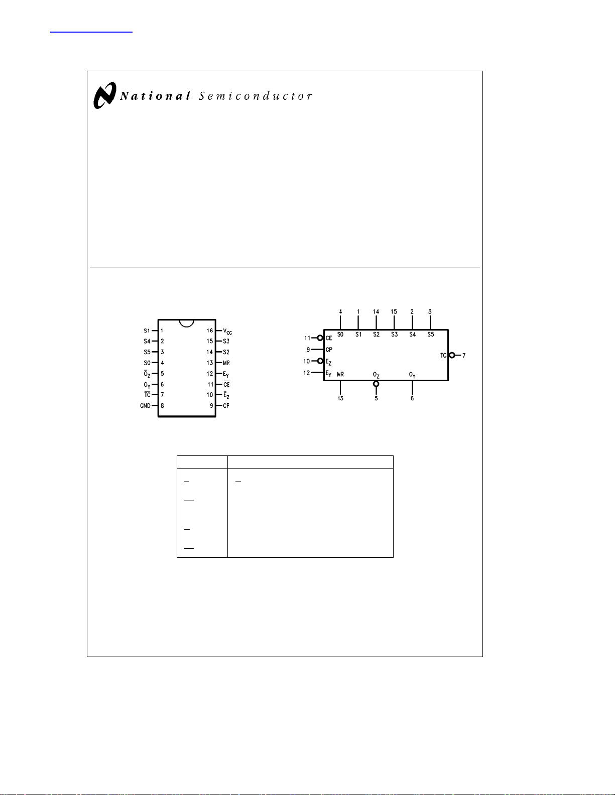
Connection Diagram
Dual-In-Line Package
Order Number 5497DMQB, 5497FMQB or DM7497N
See NS Package Number J16A, N16E or W16A
Pin Names Description
S0–S5 Rate Select Inputs
E
Z
E
Y
CE
CP Clock Pulse Input (Active Rising Edge)
MR Asynchronous Master Reset Input (Active HIGH)
O
Z
O
y
TC
OZEnable Input (Active LOW)
OYEnable Input
Count Enable Input (Active LOW)
Gated Clock Output (Active LOW)
Complement Output (Active HIGH)
Terminal Count Output (Active LOW)
TL/F/9780– 1
Logic Symbol
V
CC
GND
e
e
Pin 16
Pin 8
TL/F/9780– 2
C
1995 National Semiconductor Corporation RRD-B30M115/Printed in U. S. A.
TL/F/9780
Page 2
Absolute Maximum Ratings (Note)
The ‘‘Absolute Maximum Ratings’’ are those values
If Military/Aerospace specified devices are required,
please contact the National Semiconductor Sales
Office/Distributors for availability and specifications.
Supply Voltage 7V
Input Voltage 5.5V
Operating Free Air Temperature Range
54
DM74 0
Storage Temperature Range
b
55§Ctoa125§C
Ctoa70§C
§
b
65§Ctoa150§C
Note:
beyond which the safety of the device cannot be guaranteed. The device should not be operated at these limits. The
parametric values defined in the ‘‘Electrical Characteristics’’
table are not guaranteed at the absolute maximum ratings.
The ‘‘Recommended Operating Conditions’’ table will define
the conditions for acutual device operation.
Recommended Operating Conditions
Symbol Parameter
V
CC
V
IH
V
IL
I
OH
I
OL
T
A
Supply Voltage 4.5 5 5.5 4.75 5 5.25 V
High Level Input Voltage 2 2 V
Low Level Input Voltage 0.8 0.8 V
High Level Output Current
Low Level Output Current 16 16 mA
Free Air Operating Temperature
Min Nom Max Min Nom Max
b
ts(L) Setup Time LOW, CE to CP Rising 25 25 ns
th(H) Hold Time HIGH, CE to CP Rising 0 0 ns
th(L) Hold Time LOW, CE to CP Falling 0 0 ns
tw(H) CP Pulse Width HIGH 20 20 ns
tw(L) CP Pulse Width LOW 20 ns
tw(H) MR Pulse Width HIGH 15 15 ns
5497 DM7497
b
0.4
b
55 125 0 70
Units
0.4 mA
C
§
Electrical Characteristics Over recommended operating free air temperature range (unless otherwise noted)
Symbol Parameter Conditions Min
e
V
I
V
OH
V
OL
I
I
I
IH
I
IL
I
OS
I
CC
Input Clamp Voltage V
High Level Output V
Voltage V
Low Level Output V
Voltage V
Input Current@Max V
Input Voltage
High Level Input Current V
Low Level Input Current V
Short Circuit V
Output Current (Note 2)
Supply Current With V
Outputs High
CC
CC
e
IL
CC
e
IH
CC
CC
Clock Inputs
CC
Clock Inputs
CC
CC
eb
Min, I
e
Min, I
Max
e
Min, I
Min
e
Max, V
e
Max, V
e
Max, V
e
Max 54
e
Max
12 mA
I
e
Max,
OH
e
Max,
OL
e
5.5V
I
e
2.4V DM74 40
I
e
0.4V DM74
I
2.4 3.4 V
54 80
54
b
DM74
b
2
20
18
Typ
(Note 1)
Max Units
b
1.5 V
0.2 0.4 V
1mA
b
1.6
b
3.2
b
55
b
55
120 mA
mA
mA
mA
Page 3
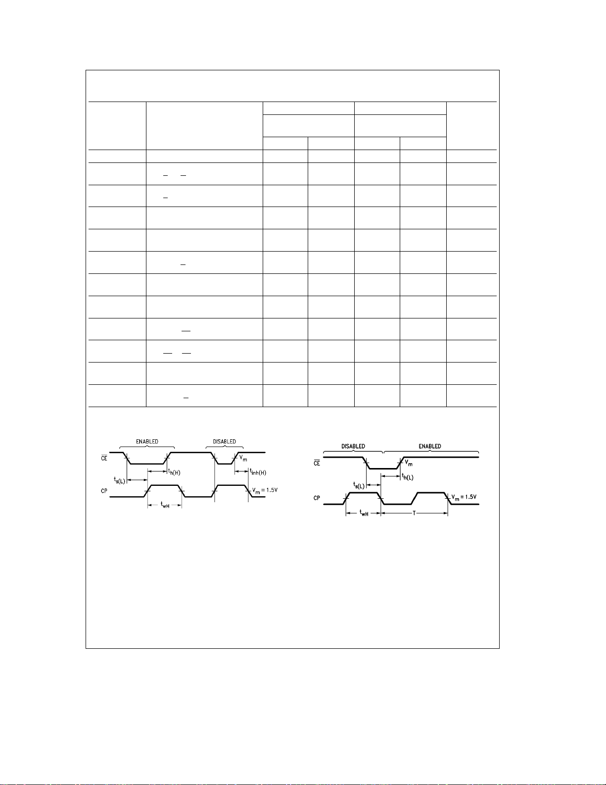
Switching Characteristics
ea
V
CC
5.0V, T
ea
25§C (See Section 1 for waveforms and load configurations)
A
Symbol Parameter
f
t
t
t
t
t
t
t
t
t
t
t
t
t
t
t
t
t
t
t
t
max
PLH
PHL
PLH
PHL
PLH
PHL
PLH
PHL
PLH
PHL
PLH
PHL
PLH
PHL
PLH
PHL
PLH
PHL
PLH
PHL
Maximum Clock Frequency 25 25 MHz
Propagation Delay 18 18
EZto O
Z
Propagation Delay 30 30
EZto O
Y
Propagation Delay 14 14
EYto O
Y
Propagation Delay 23 23
Snto O
Y
Propagation Delay 14 14
Snto O
Z
Propagation Delay 39 39
CP to O
Y
Propagation Delay 18 18
CP to O
Z
Propagation Delay 35 30
CP to TC 33 33
Propagation Delay 25 20
CE to TC 21 21
Propagation Delay
MR to O
Y
Propagation Delay
MR to O
Z
5497 DM7497
e
15 pF C
C
L
e
R
400X R
L
e
15 pF
L
e
400X
L
Min Max Min Max
23 23
33 33
10 10
23 23
14 14
30 30
26 26
43 36 ns
34 23 ns
Units
ns
ns
ns
ns
ns
ns
ns
ns
ns
Timing Diagrams
TL/F/9780– 5
TL/F/9780– 6
3
Page 4

Functional Description
The ’97 contains six JK flip-flops connected as a synchronous modulo-64 binary counter. A LOW signal on the Count
Enable (CE
initiated simultaneously by the rising edge of the clock.
When the count reaches maximum (63), with all Qs HIGH,
the Terminal Count (TC
HIGH signal on Master Reset (MR) resets the flip-flops and
prevents counting, although output pulses can still occur if
the clock is running, E
The flip-flop outputs are decoded by a 6-wide AND-OR-INVERT gate. Each AND gate also contains the buffered and
inverted CP and Z-enable (E
the Select (S0 –S5) inputs. The Z output, O
HIGH and goes LOW when CP and E
the AND gates has its other inputs HIGH. The AND gates
are enabled by the counter at different times and different
rates relative to the clock. For example, the gate to which
S5 is connected is enabled during every other clock period,
assuming S5 is HIGH. Thus, during one complete cycle of
the counter (64 clocks) the S5 gate is enabled 32 times and
can therefore gate 32 clocks per cycle to the output. The S4
gate is enabled 16 times per cycle, the S3 gate 8 times per
cycle, etc. The output pulse rate thus depends on the clock
rate and which of the S0–S5 inputs is HIGH.
Where: meS5#2
Thus by appropriate choice of signals applied to the S0 –S5
inputs, the output pulse rate can range from (/64 to $*/64 of
the clock rate, as suggested in Rate Select Table. There is
no output pulse when the counter is in the ‘‘all ones’’ condition. When m is 1, 2, 4, 8, 16 or 32, the output pulses are
evenly spaced, assuming that the clock frequency is constant. For any other value of m the output pulses are not
evenly spaced, since the pulse train is formed by interleav-
) input permits counting, with all state changes
) output will be LOW if CE is LOW. A
is LOW and S5 is HIGH.
Z
) functions, as well as one of
Z
Z
m
e
f
out
5
a
S4#2
1
a
2
S0#2
#
f
#
in
64
4
a
S3#2
0
is normally
Z
are LOW and any of
2
a
3
S2#2
a
S1
ing pulses passed by two or more of the AND gates. The
Pulse Pattern Table indicates the output pattern for several
values of m. In each row, a one means that the O
will be HIGH during that entire clock period, while a zero
means that O
period. The first column in the output field coincides with the
will be LOW when the clock is LOW in that
Z
Z
output
‘‘all zeroes’’ condition of the counter, while the last column
represents the ‘‘all ones’’ condition. The pulse pattern for
any particular value of m can be deduced by factoring it into
the sum of appropriate powers of two (e.g. 19
1) and combining the pulses (i.e., the zeroes) shown for
each for the relevant powers of two (e.g. for m
e16a2a
e
16, 2 and
1).
The Y output O
mally LOW. A LOW signal on the Y-enable input, E
ables O
y
packages can be cascaded as shown in
cuits operate from the basic clock, with the TC
is the complement of OZand is thus nor-
Y
. To expand the multiplier to 12-bit rate select, two
Figure A
, dis-
Y
. Both cir-
output of the
first acting to enable both counting and the output pulses of
the second package. Thus the second counter advances at
only (/64 the rate of the first and a full cycle of the two counters combined requires 4096 clocks. Each rate select input
of the first package has 64 times the weight of its counterpart in the second package.
a
m
m
1
e
f
out
11
Where: m
1
S1#2
e
1
e
m
2
a
S0#20(second package)
S5#2
S1#2
S5#2
a
7
a
5
a
Combined output pulses are obtained in
2
f
#
64#64
S4#2
S0#26(first package)
S4#2
in
10
4
a
a
S3#2
S3#2
9
a
3
a
Figure A
S2#2
S2#2
by letting
8
a
2
the Z output of the first circuit act as the Y-enable function
for the second, with the interleaved pulses obtained from
the Y output of the second package being opposite in phase
to the clock.
a
FIGURE A. Cascading for 12-Bit Rate Select
4
TL/F/9780– 3
Page 5

Functional Description (Continued)
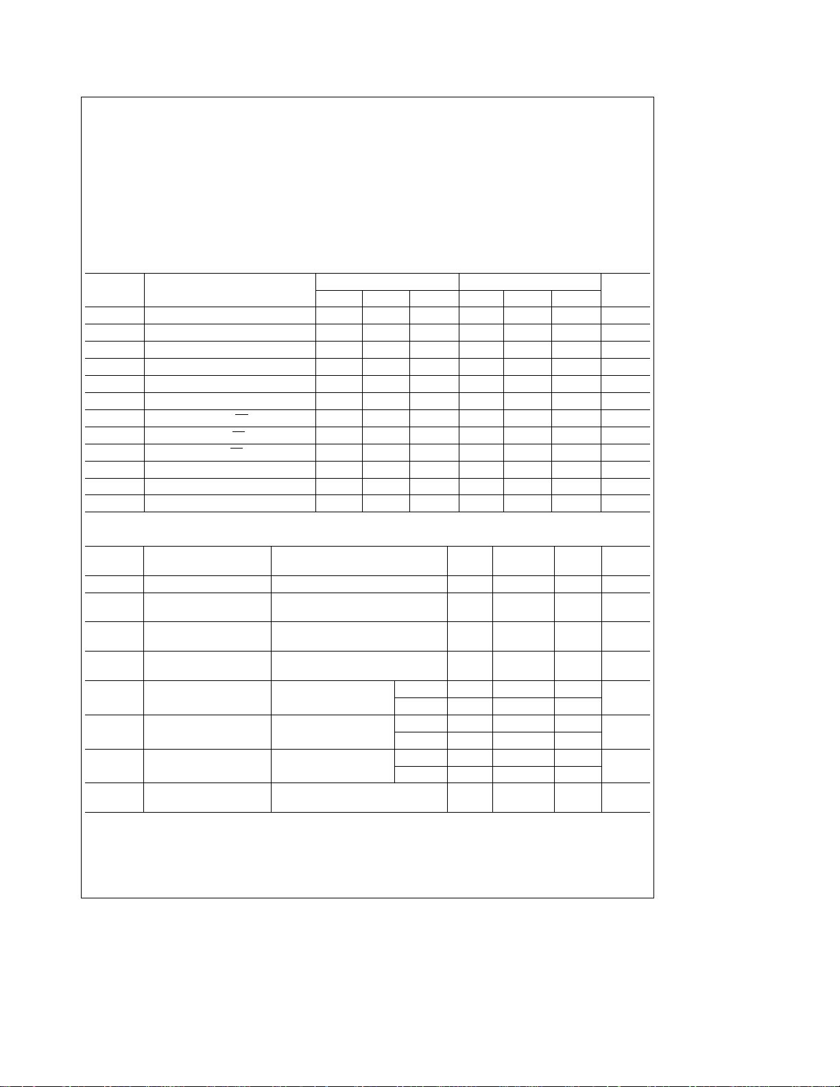
Mode and Rate Select Table (Note 1)
Inputs Clock Outputs
MR CE EZS5 S4 S3 S 2 S1 S0
Pulses
EYOYOZTC
HXHXXXXXX X HLHH 2
L LLLLLLLL 64 HLH1 3
L LLLLLLLH 64 H111 3
L LLLLL LHL 64 H2 2 1 3
L LLLLLHLL 64 H441 3
LLLLLHLLL 64 H881 3
L L L L H L L L L 64 H 16 16 1 3
L L L H L L L L L 64 H 32 32 1 3
L L L H H H H H H 64 H 63 62 1 3
L L LHHHHHH 64 LH631 4
L L L H L L L L L 64 H 40 40 1 5
HeHIGH Voltage Level
e
L
LOW Voltage Level
e
X
Immaterial
Note 1: Numerals indicate number of pulses per cycle.
Note 2: This is a simplified illustration of the clear function. CP and E
to remain HIGH.
cause O
Y
Note 3: Each rate illustrated assumes S0– S5 are constant throughout the cycle; however, these illustrations in no way prohibit variablerate operation.
Note 4: E
is used to inhibit output Y.
Y
f
Note 5: f
(32a8) f
in
e
e
m
#
out
64
40 f
in
in
e
e
0.625 f
64
64
in
also affect the logic level of OYand OZ. A LOW signal on EYwill
Z
Pulse Pattern Table
m Output Pulse Pattern at O
Z
1 1111111111111111111111111111111011111111111111111111111111111111
2 1111111111111110111111111111111111111111111111101111111111111111
3 1111111111111110111111111111111011111111111111101111111111111111
4 1111111011111111111111101111111111111110111111111111111011111111
5 1111111011111111111111101111111011111110111111111111111011111111
Notes
6 1111111011111110111111101111111111111110111111101111111011111111
8 1110111111101111111011111110111111101111111011111110111111101111
10 1110111111101111111011111110111111101111111011101110111111101111
12 1110111011101111111011101110111111101110111011111110111011101111
14 1110111011101110111011101110111111101110111011101110111011101111
16 1011101110111011101110111011101110111011101110111011101110111011
20 1011101010111011101110101011101110111010101110111011101110111011
24 1010101110101011101010111010101110101011111010111010101110101011
28 1010101010101011101010101010101110101010101010111010101010101011
32 010101... ...0101
5
Page 6

Logic Diagram
TL/F/9780– 4
6
Page 7

Physical Dimensions inches (millimeters)
16-Lead Ceramic Dual-In-Line Package (J)
Order Number 5497DMQB
NS Package Number J16A
16-Lead Molded Dual-In-Line Package (N)
Order Number DM7497N
NS Package Number N16E
7
Page 8

Physical Dimensions inches (millimeters) (Continued)
16-Lead Ceramic Flat Package (W)
Order Number 5497FMQB
NS Package Number W16A
5497/DM7497 Synchronous Modulo-64 Bit Rate Multiplier
LIFE SUPPORT POLICY
NATIONAL’S PRODUCTS ARE NOT AUTHORIZED FOR USE AS CRITICAL COMPONENTS IN LIFE SUPPORT
DEVICES OR SYSTEMS WITHOUT THE EXPRESS WRITTEN APPROVAL OF THE PRESIDENT OF NATIONAL
SEMICONDUCTOR CORPORATION. As used herein:
1. Life support devices or systems are devices or 2. A critical component is any component of a life
systems which, (a) are intended for surgical implant support device or system whose failure to perform can
into the body, or (b) support or sustain life, and whose be reasonably expected to cause the failure of the life
failure to perform, when properly used in accordance support device or system, or to affect its safety or
with instructions for use provided in the labeling, can effectiveness.
be reasonably expected to result in a significant injury
to the user.
National Semiconductor National Semiconductor National Semiconductor National Semiconductor
Corporation Europe Hong Kong Ltd. Japan Ltd.
1111 West Bardin Road Fax: (
Arlington, TX 76017 Email: cnjwge@tevm2.nsc.com Ocean Centre, 5 Canton Rd. Fax: 81-043-299-2408
Tel: 1(800) 272-9959 Deutsch Tel: (
Fax: 1(800) 737-7018 English Tel: (
National does not assume any responsibility for use of any circuitry described, no circuit patent licenses are implied and National reserves the right at any time without notice to change said circuitry and specifications.
Fran3ais Tel: (
Italiano Tel: (
a
49) 0-180-530 85 86 13th Floor, Straight Block, Tel: 81-043-299-2309
a
49) 0-180-530 85 85 Tsimshatsui, Kowloon
a
49) 0-180-532 78 32 Hong Kong
a
49) 0-180-532 93 58 Tel: (852) 2737-1600
a
49) 0-180-534 16 80 Fax: (852) 2736-9960
 Loading...