

Page 1
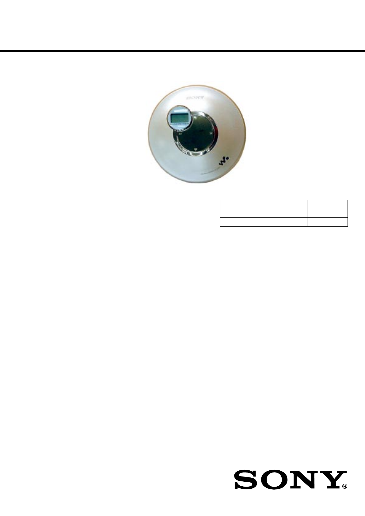
D-EJ250
SERVICE MANUAL
Ver 1.2 2004. 04
Canadian Model
AEP Model
UK Model
E Model
Model Name Using Similar Mechanism New
CD Mechanism Type CDM-3325ER
Optical Pick-up Type DAX-25E
SPECIFICATIONS
System
Compact disc digital audio system
Laser diode properties
Material: GaAlAs
Wavelength: λ = 780 nm
Emission duration: Continuous
Laser output: Less than 44.6 µW (This output is the value measured at a
distance of 200 mm from the objective lens surface on the optical pick-up
block with 7 mm aperture.)
Power requirements
• Two Sony NH-7WMAA rechargeable batteries: 1.2 V DC x 2
• Two LR6 (size AA) batteries: 1.5 V DC x 2
• AC power adaptor (DC IN 4.5 V jack): 100-240 V, 50/60 Hz
Dimensions (w/h/d) (without projecting parts and controls)
Approx. 135.8 x 22.6 x 135.8 mm (5 3⁄8 x 29⁄32 x 5 3⁄8 in.)
Mass (excluding accessories)
Approx. 182 g (6.5 oz)
Operating temperature
5°C - 35°C (41°F - 95°F)
Design and specifications are subject to change without notice.
Supplied Accessories
AC power adaptor (1)
Headphones/earphones with remote control (1)
Note on the remote control
Use only the supplied remote control. You cannot operate this CD player
with the remote control supplied with other CD players.
9-961-979-03
2004D02-1
© 2004.04
PORTABLE CD PLAYER
Sony Corporation
Parsonal Audio Company
Published by Sony Engineering Corporation
Page 2

D-EJ250
Ver 1.2
TABLE OF CONTENTS
DANGER
Invisible laser radiation when open and interlock failed or defeated.
Avoid direct exposure to beam.
CAUTION
Use of controls or adjustments or performance of procedures other
than those specified herein may result in hazardous radiation
exposure.
Flexible Circuit Board Repairing
• Keep the temperature of the soldering iron around 270°C
during repairing.
• Do not touch the soldering iron on the same conductor of the
circuit board (within 3 times).
• Be careful not to apply force on the conductor when soldering
or unsoldering.
Notes on chip component replacement
• Never reuse a disconnected chip component.
• Notice that the minus side of a tantalum capacitor may be
damaged by heat.
UNLEADED SOLDER
Boards requiring use of unleaded solder are printed with the leadfree mark (LF) indicating the solder contains no lead.
(Caution: Some printed circuit boards may not come printed with
the lead free mark due to their particular size.)
: LEAD FREE MARK
Unleaded solder has the following characteristics.
•Unleaded solder melts at a temperature about 40°C higher than
ordinary solder.
Ordinary soldering irons can be used but the iron tip has to be
applied to the solder joint for a slightly longer time.
Soldering irons using a temperature regulator should be set to
about 350°C.
Caution: The printed pattern (copper foil) may peel away if
the heated tip is applied for too long, so be careful!
• Strong viscosity
Unleaded solder is more viscous (sticky, less prone to flow)
than ordinary solder so use caution not to let solder bridges
occur such as on IC pins, etc.
• Usable with ordinary solder
It is best to use only unleaded solder but unleaded solder may
also be added to ordinary solder.
Specifications ............................................................................ 1
1. SERVICING NOTES ........................................... 3
2. GENERAL
Locating the Controls ...................................................... 3
3. DISASSEMBLY
3-1. Upper Lid ASSY, Cabinet (Upper) Sub ASSY,
Cabinet (Lower) ASSY ................................................... 4
3-2. MD ASSY (CDM-3325ER), Main Board ....................... 5
3-3. Motor ASSY (Sled) (M902),
Optical Pick-up (DAX-25E),
Turn Table Motor ASSY(Spindle) (M901) ..................... 6
4. ELECTRICAL ADJUSTMENS ..........................7
5. DIAGRAMS
5-1. Block Diagram ................................................................ 8
5-2. Printed Wiring Boards –MAIN Section (Side A)– ..........9
Printed Wiring Boards –MAIN Section (Side B)– .......... 10
5-3. Schematic Diagram –MAIN SECTION (1/3)– .............. 11
5-4. Schematic Diagram –MAIN SECTION (2/3)– .............. 12
5-5. Schematic Diagram –MAIN SECTION (3/3)– .............. 13
5-6. IC Pin Function Description ............................................ 16
6. EXPLODED VIEWS
6-1. Upper Lid Section ........................................................... 18
6-2. Cabinet Section................................................................ 19
6-3. Optical pick-up Section (CDM-3325ER) ........................20
7. ELECTRICAL PARTS LIST............................... 21
SAFETY-RELATED COMPONENT WARNING!!
COMPONENTS IDENTIFIED BY MARK 0 OR DOTTED LINE WITH
MARK 0 ON THE SCHEMATIC DIAGRAMS AND IN THE PARTS
LIST ARE CRITICAL TO SAFE OPERATION. REPLACE THESE
COMPONENTS WITH SONY PARTS WHOSE PART NUMBERS
APPEAR AS SHOWN IN THIS MANUAL OR IN SUPPLEMENTS
PUBLISHED BY SONY.
ATTENTION AU COMPOSANT AYANT RAPPORT
À LA SÉCURITÉ!
LES COMPOSANTS IDENTIFÉS PAR UNE MARQUE 0 SUR LES
DIAGRAMMES SCHÉMATIQUES ET LA LISTE DES PIÈCES SONT
CRITIQUES POUR LA SÉCURITÉ DE FONCTIONNEMENT. NE
REMPLACER CES COMPOSANTS QUE PAR DES PIÈSES SONY
DONT LES NUMÉROS SONT DONNÉS DANS CE MANUEL OU
DANS LES SUPPÉMENTS PUBLIÉS PAR SONY.
2
Page 3
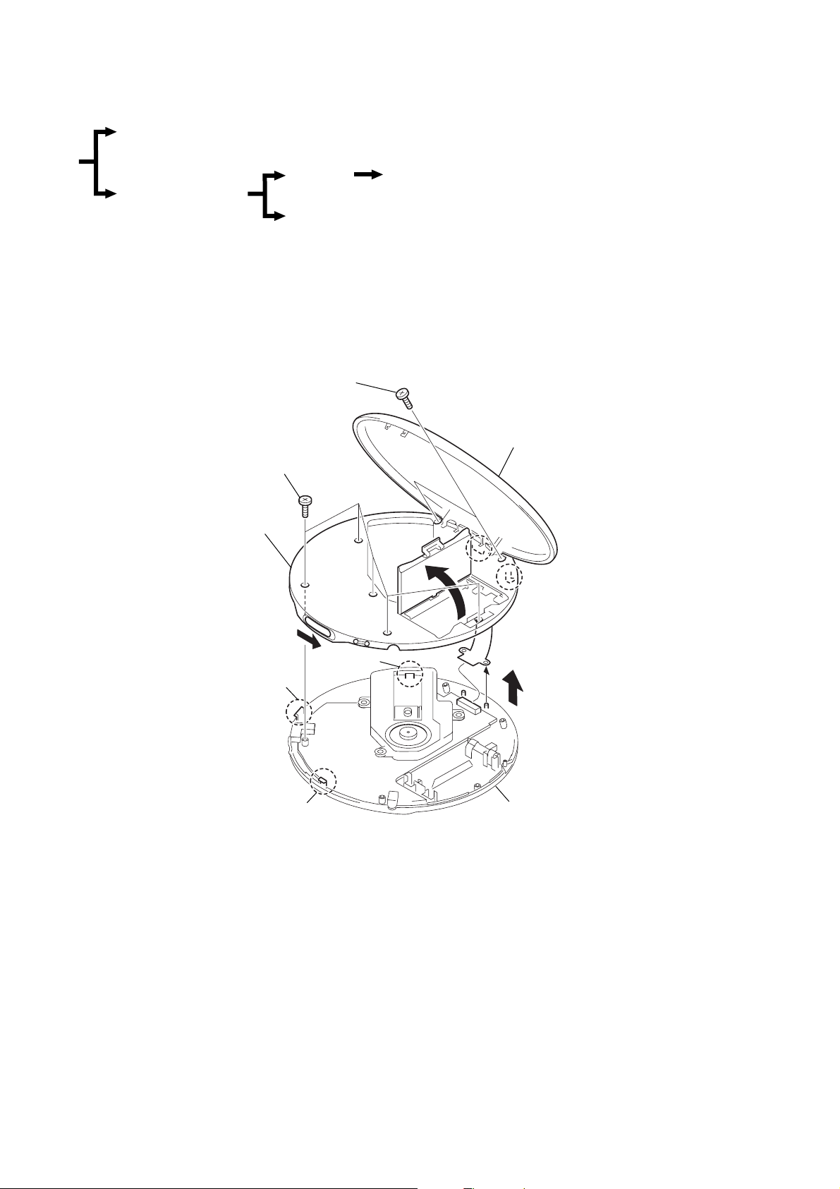
D-EJ250
y
DISASSEMBLY
z
The equipment can be removed using the following procedure.
Upper lid ASSY, Cabinet (upper) ASSY
SECTION 3
Set
MD ASSY Motor ASSY (Sled) (M902), Optical pick-up (DAX-25E),
Cabinet (lower) ASSY
Turn table motor ASSY(spindle) (M901)
Main board
Note : Follow the disassembly procedure in the numerical order given.
3-1. UPPER LID ASSY, CABINET (UPPER) ASSY, CABINET (LOWER) ASSY
4
tow screws
upper lid assy
3
five screws
cabinet (upper) assy
2
5
1
claw
5
claw
5
claw
7
CN802
6
cabinet (lower) ass
4
Page 4
SECTION 1
SERVICING NOTES
NOTES ON HANDLING THE OPTICAL PICK-UP BLOCK OR
BASE UNIT
The laser diode in the optical pick-up block may suffer electrostatic breakdown because of the potential difference generated by the charged electrostatic load, etc. on clothing and the human body. During repair, pay
attention to electrostatic breakdown and also use the procedure in the
printed matter which is included in the repair parts.
The flexible board is easily damaged and should be handled with care.
NOTES ON LASER DIODE EMISSION CHECK
The laser beam on this model is concentrated so as to be focused on the
disc reflective surface by the objective lens in the optical pick-up block.
Therefore, when checking the laser diode emission, observe from more
than 30cm away from the objective lens.
Before Replacing the Optical pick-up Block
Please be sure to check thoroughly the parameters as per the “Optical
pick-up Block Checking Procedure” (Part No. : 9-960-027-11) issued
separately before replacing the optical Pick-up block.
Note and specifications required to check are given below.
• FOK output : IC601 yg pin
When checking FOK, remove the lead wire to disc motor.
• RF signal P-to-P value : 0.4 to 0.8Vp-p
D-EJ250
Laser Diode Checking Methods
During normal operation of the equipment, emission of the laser diode
is prohibited unless the upper panel is closed while turning ON the
S809(push switch type).
The following two checking methods for the laser diode are operable.
Method :
Emission of the laser diode is visually checked.
1. Open the upper lid.
2. Push the S809 as shown in Fig. 1 .
3. Check the object lens for confirming normal emission of the laser
diode. If not emitting, there is a trouble in the automatic power
control circuit or the optical pick-up. During normal operation, the
laser diode is turned ON about 2.5 seconds for focus searching.
S809
LOCATING THE CONTROLS
CD player (front)
1 P MODE/
2 DI SPL AY/ MENU
3 u *
i (headphones)/LINE OUT jack
A
*The button has a tactile dot.
OPEN
SECTION 2
GENERAL
4 HOLD (rear)
Fig.1 Method to push S809
This section is extracted from
instruction manual.
Display
5 x/CHG
Strap hole
6 SOUND
7 ./>
DC IN 4.5 V (external power
input) jack
8 VOL +*/–
CD player (inside)
B
Open the battery
compartment lid.
Insert the # end first (for both
batteries).
3
Page 5
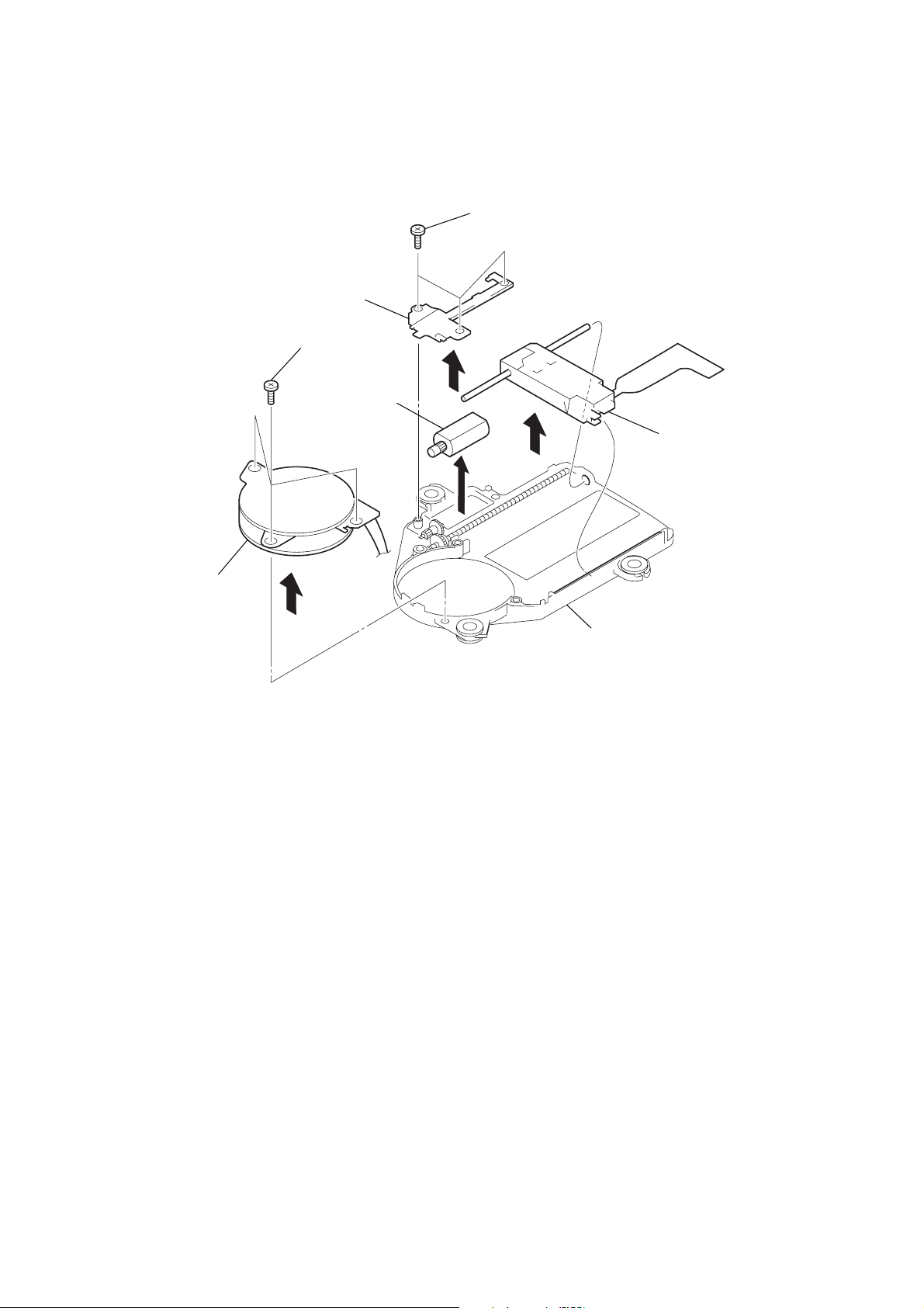
3-2. MD ASSY (CDM-3325ER), MAIN BOARD
)
D-EJ250
2
CN401
3
1
CN501
CN402
5
4
MD assy (CDM-3325ER
6
MAIN board
HOW TO SET THE HARNESS IN ASSEMBLING
CN401
CN402
harness
5
Page 6
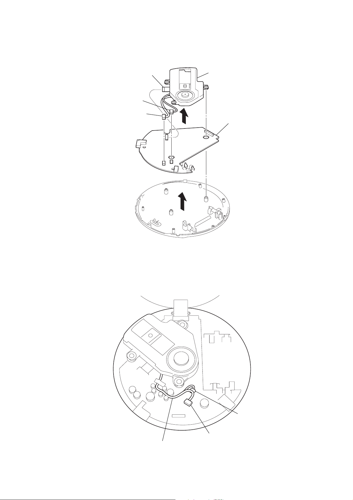
D-EJ250
p
3-3. MOTOR ASSY (SLED) (M902), OPTICAL PICK-UP (DAX-25E), TURN TABLE MOTOR ASSY (SPINDLE) (M901)
1
three screws
(B1.7x4)
3
gear cover
8
three screws
(B1.7x4)
2
5
motor assy
(sled) (M902)
4
6
7
optical pick-u
(DAX-25E)
q;
turn table motor assy
(spindle) (M901)
9
chassis
6
Page 7
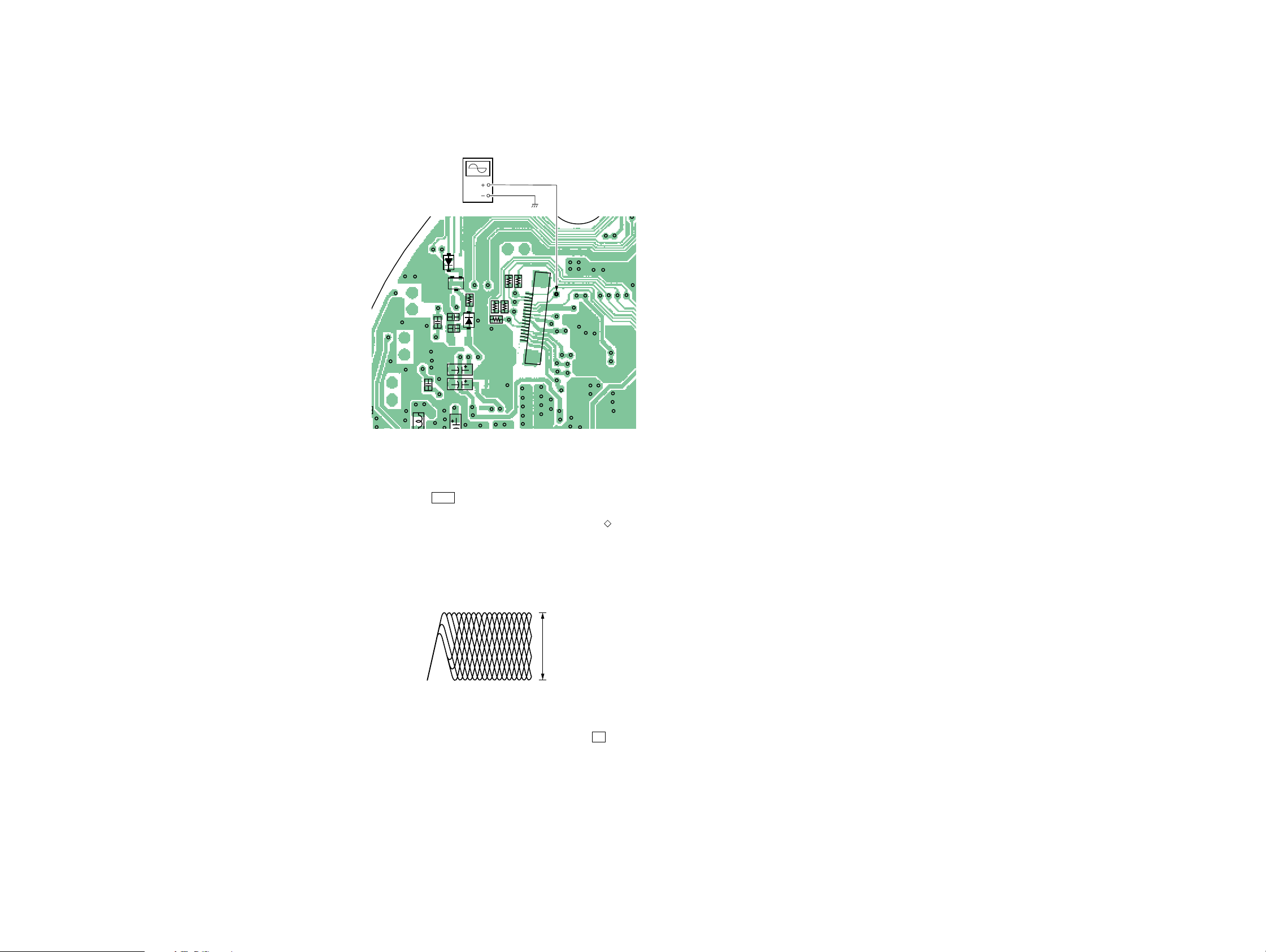
SECTION 4
)
ELECTRICAL ADJUSTMENTS
D-EJ250
The CD section adjustments are done automatically in this set.
Precautions for Check
1. Perform check in the order given.
2. Use YEDS-18 disc (Part No.: 3-702-101-01) unless otherwise
indicated.
3. Power supply voltage requirement :DC4.5 V in DC IN jack.
(J401)
VOLUME button : Minimum
HOLD switch : OFF
Focus bias Check
Condition:
• Hold the set in horizontal state.
Connection:
oscilloscope
(AC range)
[MAIN BOARD] (SIDE B)
D304
ECB
Q301
C301
C302
R316
D308
R602
C304
C206
C317
C106
R604
R650
R603
TP601(RF)
CN601
R605
15
1
TP601
(RF)
301
C307
Procedure:
1. Connect the oscilloscope to the test point TP601(RF) on the
MAIN board.
2. Set a disc. (YEDS-18)
3. Press the u button.
4. Check the oscilloscope waveform is as shown below.
A good eye pattern means that the diamond shape (
) in the
center of the waveform can be clearly distinguished.
RF Signal reference Waveform (Eye Pattern)
VOLT/DIV : 100 mV (With the 10 : 1 probe in use
TIME/DIV : 500ns
RF level
0.4 to 0.8 Vp-p
To watch the eye pattern, set the oscilloscope to AC range and
increase the vertical sensitivity of the oscilloscope for easy
watch-ing.
5. Stop revolving of the disc motor by pressing the x button.
77
Page 8
D-EJ250
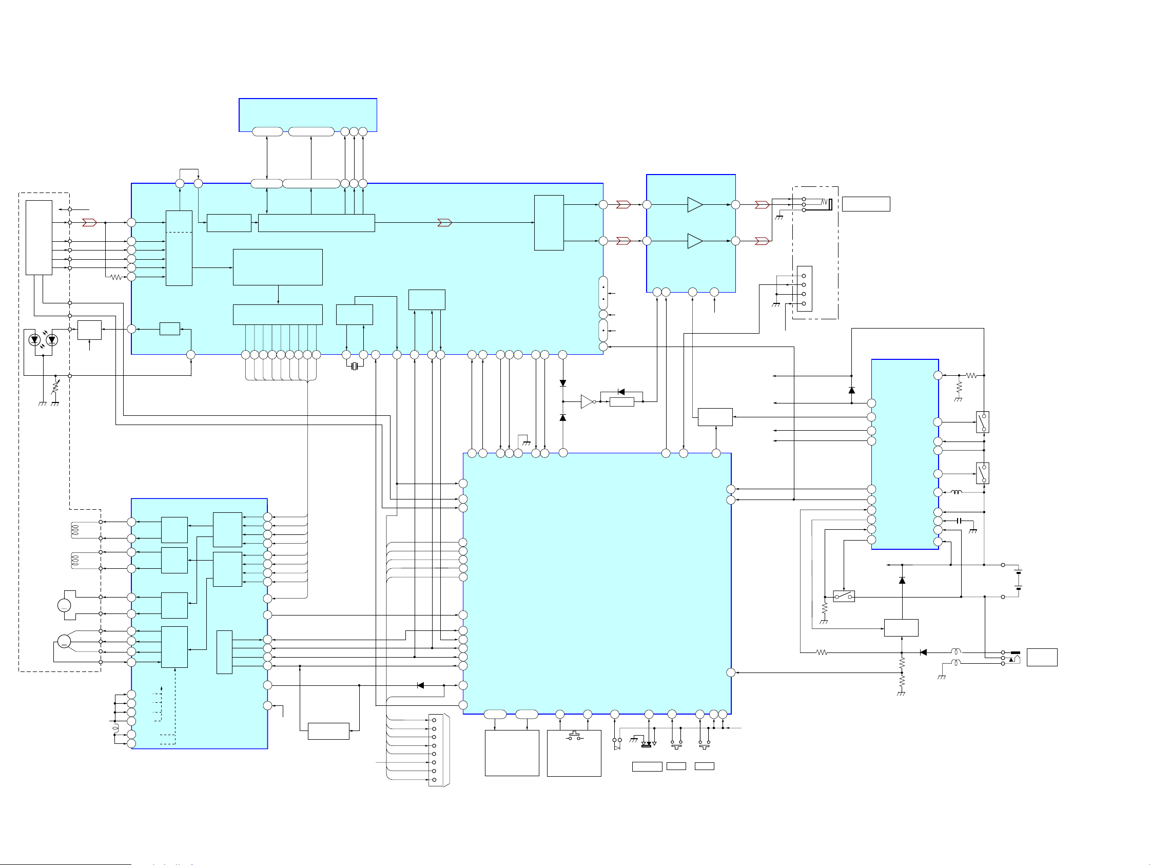
5-1. BLOCK DIAGRAM
SECTION 5
DIAGRAMS
IC603
D-RAM(16M)
OPTICAL
PICK-UP
BLOCK
(DAX-25E)
OP IC
OPGSW
VCC
OPSTB
RF
A
B
E
F
LD
PD
VCC1_2.2V
LD
DRIVER
Q601
VCC1_2.2V
D0-3 A0-10
2,3,24,25 9-12,15-19,21,8
16 17
DETI
RFGO
RFI
13
A
9
B
8
E
6
F
7
VMON
88
LD
2
APC
RF
AMP
A/D
PD
3
DEMODULATOR
87,88,84,85 97-100,96-91,82
D0-D3
EFM
SERVO
PWM
FDOP
FDON
TDOP
TDON
75 74 77 76 79 78 72 73 71 504947533738
FIN-
TIN-
FIN+
TIN+
SDOP
SIN-
SDON
SIN+
PROCESSOR
CLVON
CPOL
A0-A10
SUB CODE
CLVOP
CLKDRV
SYNC
CLVOP
XRAS
XCAS
5 23 4
90 83 89
XCAS
XRAS
CLOCK
OSC
XOUT
X601
16.934MHz
XWE
XIN
XWE
44
XRST
CLK4M
SCLK
DIGITAL SIGNAL PROCESSOR
D-RAM CONTROLLER
SIO
SDIN
SDOUT
IC601
RF AMP,SERVO
D/A CONVERTER
POFF
SRW_I
48
15
SCOR
XBUSY_O
DEFDCT_O
NC
GFS
DAC
657064524345
6711371177
FO_O
IC302
HEADPHONE AMP
LDACO LOUT
31
RDACO
36
DVDDIO
80
VCC2_2.0V
86
34
AVDD2 2.25V
DVDDV 1.5V
MUTE
35
D305
Q301
D304
74
VCHK
40
51
5
VCC1_2.2V
VCPU_1.5V
D308
DELAY
LIN
5
RIN
3
MUTE
BEEP8VCC110VCC2
161
30
26
ROUT
+V BAT
+B SWITCH
Q302,303
12
12
1429
VCPU_1.5V
VCC2_2.0V
VCC1_2.2V
VCPU_2.0V
VCPU_2.0V
D407
J302
i
/ LINE OUT
VCC2
18
VCC3
11
17
VCC1
19
VCPU 2.0V
IC403 (2/2)
POWER CONTROL
VCC0
SEM
SEO
VCC
23
22
Q406
20
16
FOCUS
COIL
TRACKING
COIL
M902
SLED
MOTOR
M901
SPINDLE
MOTOR
GFS_I
IC403 (1/2)
FOCUS/TRACKING COIL DRIVE
SLED/SPINDLE MOTOR DRIVE
FIN3
FIN+
F+
F-
T+
T-
S+
M
M
S-
W
V
U
+VBAT
L403
44
42
48
46
52
50
6
4
2
80
53
49
45
41
1
5
FO3
RO3
FO2
RO2
FO1
RO1
W
V
U
COMCOM
VM1
VM12
VM23
VM3
SPVCC1
SPVCC2
CH3
H
BRIDGE
CH2
H
BRIDGE
CH1
H
BRIDGE
CH4
H
BRIDGE
LEVEL
SHIFTER
LEVEL
SHIFTER
I/F
RIN3
FIN1
RIN1
FIN2
RIN2
BRK
PWM
SYNC
LATCH
DATA
CLOXK
WAKEUP
RESET_O
XRST
60
FIN-
59
SIN+
56
SIN-
55
TIN+
58
TIN-
57
CPOL
70
SLVOP
72
SYNC
34
74
FG
40
39
38
37
35
36
VCC2_
2.0V
DEFFERENTIAL
Q407
VCPU_2.0V
CLK4M
RESET2
PGM_SEL
PGM_SCK
PGM_SDTI
PGM_SDTO
RESET2
TEST
CLK4M
D802
1
2
3
4
5
6
7
9
SRW_O
POFF_O
XIN
2
OPGSW_O
79
XOPSTBY_O
78
73
< PGMSEL_O >/SC_SEL_O
69
PGM_SCK_O
68
PGM_SDTI_I
67
PGM_SDTO_O
4
TEST
FG I
72
XPOWLT_O
14
SDTI_I
16
SDTO_O
17
SCK_O
18
XWAKEUP_O
66
8
XREST_I
XRST_O
76
56-42 60-57
CN801
TEST
CONNECTOR
SEG0
I
SCOR_I
XBUSY_I
SEG14
LCD801
LIQUID
CRYSTAL
DISPLAY
DEFECT_I
COM0
I
COM3
FOK_I
KEY MATRIX
S1005
S1007
AMUTE_O
IC801
SYSTEM
CONTROL
MICOM
WP/AD_KEY_1
AD_KEY_2
2523 28 40
S1001
|
|
S1004
WP/XOPEN
S809
(OPEN)
HOLD_I
S810
.
HOLD
t
OFF ON
BEEP_O
AD_CHGMNT
WP/AD_RMKEY
AD_BATMNT
WP/AD_DCINMNT
VOL+_IN
35
S802
VOL+
VOL-_IN
38
S803
VOL-
HPSW_O
22
24 66
27
AVCPU
ADVREF
19
20
VCPU_2.0V
Q401
CHARGE
SWITCH
67
61
62
63
65
+VBAT
CHGMNT
VMMNT
DCIN
REGB
DET
CHGB
D405
SWITCH
Q402, 403
25
STNG
LG
8
L404
12
VIN
68
BATM1
BATM2
69
DCIN_S
64
D402
L401
L402
• Signal path.
E : CD PLAY
Q404
DRY BATTERY
SIZE "AA"
(IEC DESIGNATION LR6)
2PCS, 3V
J401
DC IN 4.5V
!
8
8
Page 9

D-EJ250
5-2. PRINTED WIRING BOARDS – MAIN SECTION (SIDE A) –
1
2
3 4 5 6 7
(SIDE A)BOARDMAIN
A
C815
R807
TP804
R903
R906
R909
R912
R915
R918
TP808
TP821
TP820
SL801
R803
R902
R905
R908
R911
R914
R917
40 21
41
60
61
C801
C802
R830
C809
R833
C804
C811
C814
R838
R827
IC801
R825
R832
C805
80
CN801
R836
C813
20
1
CONNECTOR
TP807
TP805
TP810
TP805
B
TP801
TP818
TP813
TP816
TP815
TP817
R904
R907
R910
R913
R916
R919
R920
TP802
TP805
TP803
TP812
C
D
E
F
L604
R845
R804
R849
C812
R805
R841
C806
D803
C807
C810
SL802
1
TEST
R802
R811
BP801
10
DRY BATTERY
(IEC DESIGNATION LR6)
: Uses unleaded solder.
D601
C622
R628
R619
51
C626
R615
50
R622
IC601
75
76 100
C621
C620
26 14
R446
R401
C627
1
C623
TP407
TP402
R620
BP807
R854
R858
R859
D802
SIZE "AA"
2PCS, 3V
R618
C629
R631
BP803
R616
X601
L602
C632
IC603
FB406
C414
BT402
C635
C630
C618
26
R447
C625
25
Q401
D405
C639
1
C631
C640
R609
C608C613
C614
C605
R611
TP414
R407
ECB
R617
R610
13
C405
C607
R613
C604
C612
R612
TP413
R403
R408
TP403
D410
C637
Q601
ECB
C410
C636
C609
TP410
C606
C634
R601
C610
TP404
L601
R608
D403
C412
R301
BCE
Q302
TP409
C447
40 21
41
60
61
C419
C420
C426
C407
R409
BCE
Q303
FB408
C418
TP605
TP601
TP602
TP603
C638
L302
C448
IC403
C421
R614
FB405
R438
C440
R621
TP406
C437
C432
80
C422
C633
C104
20
1
C423
TP608
TP607
R101
R201
C204
116
IC302
89
C306
C220
C434
C436
C403
C413
C450
C433
C429
C425
R320
TP613
TP614
R305
C305
R311
R310
C409
C205
TP301
C107
R103
R105
C105
C207
C308
R203
FB301
R313
TP411
FB303
D306
R205
D301
D302
TP823
TP201
D101
HOLD
OFF
t
ON
D201
S810
D303
8
.
J302(1/2)
i/LINE OUT
9
• Semiconductor
Location
Ref. No. Location
D101 D-8
D201 D-8
D301 D-8
D302 D-8
D303 D-8
D306 D-8
D403 F-5
D405 F-5
D410 F-5
D601 A-4
D802 D-4
D803 C-3
IC302 C-7
IC403 E-6
IC601 B-4
IC603 C-5
IC801 C-3
Q301 B-3
Q302 D-6
Q303 C-6
Q401 F-5
Q601 B-5
J401
DC IN 4.5V
G
R406
S802
VOL+
S803
VOL–
11
1-860-875-
(11)
99
Page 10

D-EJ250
PRINTED WIRING BOARDS – MAIN SECTION (SIDE B) –
R204
2
D304
ECB
Q301
C304
C206
C317
C106
C301
L301
R322
R104
L305
C307
1
A
OPTICAL PICK-UP
BLOCK
DAX-25E
B
C
J302(2/2)
: Uses unleaded solder.
3 4 5 6 7
(SIDE B)BOARDMAIN
CN601
R605
R604
15
R316
D308
C302
R650
R602
R603
R315
TP601
(RF)
1
L605
C803
R810
D805
R808
CN802
R809
8
9
• Semiconductor
Location
24
1
R880
Ref. No. Location
D304 B-3
D308 B-3
D402 F-4
D404 E-5
D407 E-3
D409 E-4
D805 B-7
Q402 F-4
Q403 E-5
Q404 E-3
Q406 E-3
Q407 E-4
R448
D
C318
FB401
R801
FB403
R812
LCD801/
KEY MATRIX
FB302
R314
S809
(OPEN)
E
R871
R816
R872
C808
R864
F
R421
R444
R863
D407
R439
L405
R457
C428
BCE
Q406
L407
L403
FB404
BCE
Q404
4
1
CN402
FB402
R404
R440
R428
D409
L404
L411
C438
R419
C435
C445
R436
C427
R434
L402
C441
2
1
CN401
ECB
R427
Q407
Q402
ECB
D402
L409
L401
L406
R412
C415
R411
R416
R413
Q403
BCE
D404
M
M
M902
SLED
MOTOR
M901
SPINDLE
MOTOR
G
11
1-860-875-
10
(11)
10
Page 11

5-3. SCHEMATIC DIAGRAM – MAIN SECTION (1/3) –
Q601
CN601
15P
OPGSW
OPSTB
F+
TT+
F-
C638
R612
2SB167900LSO
LD DRIVER
L601
µH
10
R601
R650
1
0
C412
47
6.3V
R409
2.2
100k
R608
2.2
R610
C610
100k
4.7
R611
2.2k
C631
1M
R602
100k
R603
100k
R604
100k
R605
100k
C634
1000p
C604
0.1
C606
10
C605
1000p
C612
1000p
C613
0.01
C614
C607
C608
C609
1
0.1
6.3V
2200p
0.1
0.22
R613
470
R614
D-EJ250
BATMNT
BUS 1
VCC2
A2
A3
A0
A1
A10
A3
A2
A0
A1
A4
D1
XOUT
A5
A5
D0
D0
DVSSIO
A7
A6
A7
A6
A8
C621
0.1
D3
D2
D3
DVDDIO2(2.4V)
DOCKI
DVDD(1.5V)
R622
1k
C622
0.01
R628
10k
A10
A8
D2
DVSS1
IC603
MSM51X17400F-10TFSR1
D-RAM(16M)
A3
A2
A1
A0
A4
A5
A6
A2
A3
A1
A0
A4
A5
A6
AVDD(2.0V)
LD
PD
VMON
VCHK
E
F
B
A
SVSSI
BIAS
NC
RFI
PKC
BTC
RFGO
DETI
ASYI
ASYO
MON1
MON2
ADPFO
ADPFI
FCO
PCO
RLINO
AVSS2
C639
2.2
C618
2.2
R609
C633
6.3V
2.2k
100
C636
100p
C637
100p
R621
0
47
RLINI
RDACO
VCDACO
LDACO
C640
2.2
C630
0.01
R617
2.2k
DIGITAL SIGNAL PROCESSOR
LLINI
16.934MHz
C635
VCC
VSS
A7
A9
A8
XWE
XRAS
A7
A8
A9
XWE
XRAS
IC601
BU9354CKV
RF AMP,SERVO
D-RAM CONTROLLER
D/A CONVERTER
LLINO
AVDD2(2.25V)
MUTE
DVDDIO(2.0V)
XIN
R615
0
R616
1M
X601
D601
RSB6.8STE61
0.01
A4
D1
XCAS
XCAS
SCOR
SCOR
XRAS
XRAS
XOI
A9
A9
A10
DVSSIO2
A10/CAS2B
POFF
XRST
POFF
XRST
D1
D0
XWE
D1
D0
XWE
D2
XCAS
D3
D2
XCAS
D3
C620
0.1
SIN-
SIN+
SDOP
SDON
DVDDIO(2.0V)
SCLK
DVSSIO
SRW
1k
1k
R618
R620
SCK
SRW
VCC
VSS
TIN+
TIN-
TDOP
TDON
FDOP
FDON
CLVOP
CLVON
CLKDRV
GFS
EXPCLK
TEST S
EFM/YFLG
C2FX
FOK O
DEFECT O
LRCKI
DOUTAI
LRCKO
DOUTAO
DOCKO
TEST
TDO
TMS
TCK
CLK4M
XBUSY O
DVDD(1.5V)
SDIN
SDOUT
1k
R619
SDTO
SDTI
C627
TDI
22
4V
C626
0.1
L605
R447
0
C623
1
R401
10
R631
L602
C625
0.01
C632
0.1
R446
0
FIN+
FIN-
CPOL
GFS
FOK
L604
1k
0
CLK4M J
XBUSY
C629
22p
0
0
0
L305
VCPU
AU GND
COMP
GND-2
BEEP
AMUTE
HP L
1SS355TE-17
R320
100k
R311
220k
D304
C302
R315
R305
220k
C301
6.3V
C305
6.3V
0
4.7
22
22
Q301
DTC144TUA-T106
BUFFER
D308
1SS355TE-17
C317
2.2
R201
2.2k
6.3V
R101
2.2k
L302
0
Q303
2SB167900LSO
+B SWITCH
R301
22k
Q302
DTC144TUA-T106
+B SWITCH
C204
470p
C104
470p
C220
C304
0.01
220
WPSW
BUS 4
R310
0
R316
22k
IC302
AN17020B-E1
HEADPHONE AMP
BEEP
MUTE
HP/L
R IN
GND
L IN
RIP F1
CR
VCC1
C306
0.01
4V
R322
10
RMKEY
OPEN
HOLD
R314
RIP F2
1k
FB301
R872
10k
GA R
ROUT
GND
LOUT
GA L
VCC2
0
C808
4700p
R871
220k
R313
C206
2.2
C106
2.2
L301
47
C307
22
4V
D302
D306
UDZSTE-175.1B
10k
FB302
SL805
R816
10k
C205
220
4V
C105
220
4V
µH
C308
100
6.3V
D301
UDZSTE-175.1B
UDZSTE-175.1B
0
C207
0.01
R203
220
R103
220
C107
0.01
RSB6.8STE61
OFF
ON
D101
HOLD
R204
10k
R205
FB303
R105
R104
10k
S810
0
0
0
C318
1000p
D201
RSB6.8STE61
D303
RSB6.8STE61
S809
(OPEN)
J302
/LINE OUT
BUS 2
VCC1
A GND
VCC4
11 11
BUS 3
SYNC
PWM
VCC3
VIN
Page 12

D-EJ250
Ver 1.2
5-4. SCHEMATIC DIAGRAM – MAIN SECTION (2/3) –
VCPU
VCC2
BATMNT
BUS 1
GND-2
COMP
AU GND
WPSW
BUS 4
BUS 5
D AU GND
D GND
CN802
24P
1
5
10
15
20
24
R448
RSB6.8STE61
0
R880
D805
R801
0
0
SEG14
SEG13
SEG12
SEG11
SEG10
SEG9
SEG8
SEG7
SEG6
SEG5
SEG4
SEG3
SEG2
SEG1
SEG0
COM3
COM2
COM1
COM0
KEY 1
KEY 2
• See page 16 for IC Pin Function Description.
VOL-
HOLD
VOL-
TEST
HOLD I
LCD REQ O
15
SEG14
SEG13
SEG12
SEG11
SEG10
SEG9
SEG8
SEG7
SEG6
SEG5
SEG4
SEG3
SEG2
SEG1
SEG0
COM3
COM2
COM1
COM0
R902
R903
R904
R905
R906
R907
R908
R909
R910
R911
R912
R913
R914
R915
R916
R917
R918
R919
R920
10k
10k
10k
10k
10k
10k
10k
10k
10k
10k
10k
10k
10k
10k
10k
10k
10k
10k
10k
SEG
SEG
SEG
SEG
SEG
SEG
SEG
SEG
SEG
SEG
SEG
SEG
SEG
SEG
SEG
SEG
COM
COM
COM
COM
14
13
12
11
10
9
8
7
6
5
4
3
2
1
0
3
2
1
0
C1
V2
V1
V3
VOL+
22k
R803
VOL+
X4M/16M I
XWAKEUP O
C0
0.01
470p
C812
C811
TU ON I
WP/K2 RM
VDD EEPROM
T5AW5-04CD
CONTROL
PGM SDTI
PGM SCK O
PGM SDTO
BEEP
0.01
C809
NC
IC801
SYSTEM
MICOM
CD ON
OPEN
RMKEY
DCINMNT
0
0
10k
R830
R832
R827
BEEP O
TUPWR O
WP/XOPEN
AD DCINMNT
AMUTE 0
FG I
<PGMSEL 0>/SC SEL O
GFS I
KEY 2
KEY 1
10k
10k
0
R838
R833
R836
AD KEY 2
AD BATTMNT
WP/AD KEY 1
WP/AD RMKEY
XOPSTBY O
XRESET O
POFF O
RESET TU 0
R845
100k
CHGMNT
100k
0.1
R841
C813
AD SEL
AD CHGMNT
XPOWLT
DSP SEL
CD/TU
OPGSW O
0.01
C814
ADVREF
AVCPU
SCK
SDTO
SDTI
SRW
HPSW
SCOR
HP
ACKCD
RESET
XBUSY
FOK
VCPU 2V
TEST
XOUT
C805
0.01
XIN
GND
R804
O
O
I
O
O
O
I
L
I
I
I
I
S803
VOL-
R864
*R804
100K
*
220K
C810
0.1
CND,E18,HK,TH
AEP,UK,EE
C807
0.22
0
R854
R858
R859
D803
UDZSTE-175.1B
R811
S802
10k
R849
1k
R805
100k
R802
220k
0
0
22k
VOL+
R863
22k
SDTO
SRW
POWERLT
SCOR
RESET
XBUSY
CLK4M J
SCK
SDTI
HP L
FOK
C806
0.01
D802
MA2ZD14001S0
PGM SEL
PGM SCK
PGM SDTI
PGM SDTO
RESET2
CLK4M J
CN801
10P
TEST
CONNECTOR
R810
C801
R807
0
0
0.1
C815
0.1
C802
0.1
C803
0.1
C804
0.22
R808
100k
XWAKEUP
PGM SDTI
PGM SDTO
R809
100k
12
PGM SCK
R825
0
GFS
FG
R812
PGM SEL
0
AMUTE
12
XRST
POFF
OPSTB
OPGSW
RESET2
CLK4M J
Page 13

5-5. SCHEMATIC DIAGRAM – MAIN SECTION (3/3) –
BUS 5
CN401
2P
D GND
D AU GND
A GND
M
PW
BUS 3
BUS 2
SYNC
VIN
VCC1
VCC4
VCC3
BATMNT
COMP
D-EJ250
BUS 1
GND-2
F-
F+
T-
T+
AU GND
0
FB402
VCC2
VCPU
2SD1781K-T146-QR
CHGMNT
DCINMNT
Q401
CHARGE
SWITCH
R403
1
R413
47k
R411
220k
C415
0.22
R407
2.2
Q402
2SA1363-T111-1E
SWITCH
R408
100
D405
RB160M-30TR
R412
47k
FB403
0
R416
220
2SC4154TP-1F
FG
D404
MA111-TX
Q403
SWITCH
C418
C419
C420
FB401
0.1
0.022
0.022
R419
10k
µH
L406
RO1
VCC3
VM12
VIN
FO2
DSW
47
PGND2
ERGND
POW
0
C421
C422
C423
CPOL
4700p
4700p
4700p
FIN+
FIN3
DCIN
REGB
DET
DCIN S
CHGB
VMMNT
CHGMNT
BATM1
BATM2
BBK
PREGND
PWM
SOFTPWM
FG
CSL2
CSL1
W1
V1
U1
COM
SPVCC
FIN-
RIN3
U OUT
SIN-
TIN-
SIN+
TIN+
FIN1
FIN2
RIN2
RIN1
0GND
FOCUS/TRACKING COIL DRIVE
SLED/SPINDLE MOTOR DRIVE
POWER CONTROL
OUT
W
SPGND2
V OUT
SPVCC2
SPGND1
FO1
VM1
IC403
BH6580KV
LG
VG
PGND1
SSW
RO2
VM23
VCC0 2.25V
USW
µH
L409
47
FO3
RO3
PGND3
WAKEUP
RESET O
PREGND
VCC2NF
VCPUNF
VCC2 2.0V
VCC1 2.25V
VCPU 2.0V
VM3
LATCH
DATA
CLOXK
XRST
SYNC
SOFT
SLOW
PMG
STNG
SEP
SEM
SEO
GSW
VCC
C438
EI
EO
R406
R434
100k
D409
VARISTOR
POWERLT
XWAKEUP
C441
0.22
XRST
SDTO
SCK
RESET
R427
47k
R404
0
0
FB404
0
FB405
0
FB406
0
FB408
C435
L411
22
47µH
10V
1
R440
47k
C414
0.01
0
R436
C427
R457
10k
C447
1000p
C440
2200p
R421
10k
R438
10k
R439
47k
C409
4.7
0.01
C448
0.047
R444
100k
C445
1
Q407
2SC4081T106R
DEFFERENTIAL
MA111-TX
DRY BATTERY
SIZE"AA"
(IEC DESIGNATION LR6)
2PCS,3V
CN402
4P
J401
DC IN 4.5V
D402
RB160M-30TR
L401
4.7µH
L402
4.7µH
C405
D410
RSB6.8STE61
1
C407
1
L403
47µH
C410
1
D403
MA2YD2300LS0
C425
µH
100
L407
22
10V
1
2SB167900LSO
C434
47
4V
C426
220
6.3V
L404
220µH
L405
220µH
C428
4.7
16V
C429
0.1
C450
C413
1
C403
22
6.3V
C432
220
1
4V
C433
2SA1602TP-1F
SWITCH
Q404
SWITCH
C436
47
4V
Q406
C437
47
4V
R428
100k
D407
1SS355TE-17
13 13
Page 14

D-EJ250
p
p
p
p
Ver 1.2
For Schematic Diagrams:
Note:
• All capacitors are in µF unless otherwise noted. pF µµF 50 WV or
less are not indicated except for electrolytics and tantalums.
• All resistors are in Ω and 1/
• f : internal component.
Note:
The components identified by mark 0 or dotted
line with mark 0 are critical for safety.
Replace only with part
number specified.
W or less unless otherwise specified.
4
Note:
Les composants identifiés par
une marque 0 sont critiques
pour la sécurité.
Ne les remplacer que par une
piéce portant le numéro
spécifié.
• A : B+ Line.
• Power voltage is dc 4.5 V and fed with regulated dc power supply
from battery terminal.
•Voltages are taken with a VOM (Input impedance 10 MΩ).
Voltage variations may be noted due to normal production tolerances.
•Waveforms are taken with a oscilloscope.
Voltage variations may be noted due to normal production tolerances.
• Circled numbers refer to waveforms.
• Signal path.
E : CD PLAY
• Abbreviation
CND : Canadian model.
E18 : AC100-240 V Area in E model
EE : East European model
HK : Hong Kong model
TH : Thai model
For Printed Wiring Boards:
• X : parts extracted from the component side.
• a : Through hole.
• f : internal component.
• : Pattern from the side which enables seeing.
(The other layers' patterns are not indicated.)
Caution:
Pattern face side: Parts on the pattern face side seen from
(Side B) the pattern face are indicated.
Parts face side: Parts on the parts face side seen from
(Side A) the parts face are indicated.
• Abbreviation
CND : Canadian model.
E18 : AC100-240 V Aarea in E model
EE : East European model.
HK : Hong Kong model.
TH : Thai model.
• IC BLOCK DIAGRAM
IC302 AN17020B-E1
MUTE
1
HEADPHONE
HP/L
R-IN
GND
L-IN
RIP-F1
VCC1
2
3
4
5
6
7
CR
8
/LINE
SWITCH
MUTE
RF1
BEEP
16
BEEP
15
GA-R
–
+
+
–
RF2
14
ROUT
13
GND
12
LOUT
11
GA-L
VCC2
10
9
RIP-F2
•WAVEFORMS
IC403 qd DSW
1
5.7 µsec
IC403 ef SYNC
2
5.7
µ
sec
IC601 qd RFI
3
3.0 Vp-
VOL/DIV : 1 V AC
TIME/DIV : 2 µsec
2.0 Vp-p
VOL/DIV : 1 V AC
TIME/DIV : 2 µsec
0.4 to 0.8Vp-p
VOL/DIV : 0.5 V AC
TIME/DIV : 0.5 µsec
IC601 ek XOUT
4
16.934 MHz
IC601 td CLK4M
5
0.237 µsec
IC801 2 XIN
6
0.237 µsec
2.0 Vp-
VOL/DIV : 1 V AC
TIME/DIV : 50 nsec
2.3 Vp-
VOL/DIV : 1 V AC
TIME/DIV : 0.2 µsec
2.3 Vp-
VOL/DIV : 1 V AC
TIME/DIV : 0.2 µsec
IC601 BU9354CKV
AVDD1 (2.0V)
VMON
VCHK
AVSS1
BIAS
N.C.
PKC
BTC
RFGO
DETI
ASYI
ASYO
MON1
MON2
ADPFO
ADPFI
FCO
PCO
1
LD
2
PD
E
F
B
A
RFI
APC
3
4
A/D
5
6
7
8
9
10
11
12
13
14
15
16
17
18
19
20
21
22
23
24
25
RF
AMP
D/A
PLL
A399A298A197A096A495A594A693A792A891A990XRAS88D187D086DVDDIO2 (2.4V)
100
SERVO CORE
WINDOW ECC
1bit DAC
CLOCK
GEN
ESP
XWE
89
85D384D283
SUB SIO
XCAS82A10/CAS2B81DVSSIO280DVDDIO (2.0V)
SDOP78SDON77TDOP76TDON
79
PWM
FLAG
FDOP
75
FDON
74
CLVOP
73
CLVON
72
CLKDRV
71
GFS
70
EXPLCK
69
TEST_S
68
EFM/YFLG
67
C2FX
66
FOK_O
65
64
DEFECT_O
63
LRCKI
62
DOUTAI
61
LRCKO
DOUTAO
60
59
DOCKO
58
TEST
TDO
57
TDI
56
TMS
55
TCK
54
CLK4M
53
XBUSY_O
52
DVDD (1.5V)
51
28
29
26
27
30
31
32
33
34
35
36
37
38
39
40
41
42
43
44
45
46
47
48
49
50
RDACO
VCDACO
LLINI
LDACO
LLINO
RLINI
RLINO
AVSS2
14
14
XIN
MUTE
DVDDIO (2.0V)
AVDD2 (2.25V)
XOUT
DVSSIO
DVDD (1.5V)
DOCKI
DVSS1
SCOR
XRST
POFF
DVSSIO
SCLK
SRW
SDIN
SDOUT
Page 15

IC403 BH6580KV
61
60
DCIN
59
58
57 56
55
54 53 51 50 49 47 46 454852
36
35
34
32
31
30
33
23
22
29
27
26
25
24
28
21
91 2 3 4 7 85 6 10 11 12 13 14 15 16
62
REGB
63
DET
64
DCIN_S
65
CHGB
66
VMMNT
67
CHGMNT
68
BATM1
69
BATM2
70
BBK
71
PREGND
72
PWM
73
SOFTPWM
74
FG
75
CSL1
SPVCC1
U_OUT
SPGND1
V_OUT
SPVCC2
W_OUT
LG
SPGND2
VG
SSW
VCC3
VIN
DSW
POWERGND
USW
VCC0_2.25V
17
VCC1_2.25V
18
VCC2_2.0V
20
VCC
FIN3
RIN3
FIN2
RIN2
FIN1
RIN1
VM1
0GND
FO1
PGND1
VM12
RO1
FO2
PGND2
RO2
VM23
44
FO343PGND342RO341VM3
76
WI
PRE DRIVE
LOGIC
VG
VCC
VG
SLOPE
SIGNAL
77
VI
78
UI
79
COM
80
CSL2
XRST
37
WAKEUP
38
CLOXK
39
DATA
40
LATCH
RESET_O
SYNC
PREGND
EI
SOFT
SLOW
EO
PMG
VCPUNF
VCC2NF
STNG
SEP
SEM
SEO
GSW
INPUT
SELECT
CHARGE
CONTROLLER
LEVEL
SHIFTER
HVPROT
MONTOR
AMP
VM
VCC
VG
VG
VCC3
CH1
H BRIDGE
CH2
H BRIDGE
CH3
H BRIDGE
INTERFACE
RESET
CLK
SAW GEN
VG
VCC
VCC2
19
VCPU_2.0V
10msec
DELAY
VCC4
D-EJ250
15
Page 16

D-EJ250
5-6. IC PIN FUNCTION DESCRINTION
• IC801 (SYSTEM CONTROL) T5AW5-04CD
Pin No. Pin Name I/O Description
1 GND – Ground terminal
2 XIN I System clock input
3 XOUT O Not used (OPEN)
4 TEST I Test mode terminal
5 VCPU_2.0V – Power supply
6 FOK_I I Focus OK signal input
7 XBUSY_I I Auto sequencer status signal input from BU9354CKV
8 RESET_I I Micon reset input
9 ACKCD_I I Not used (Fixed to L)
10 HP-L O Headphone/line switch signal output to AN17020B
11 SCOR_I I SCOR pulse input
12 HPSW_O O Headphone power switch signal output
13 DSP_SEL I DSP select signal input (Fixed to L)
14 XPOWLT_O O Data latch signal output to BH6580KV
15 SRW_O O Serial interface Read/Write signal output to BH9354CKV
16 SDTI_I I Serial data input from BU9354CKV
17 SDTO_O O Serial data output to BU9354CKV
18 SCK_O O Serial clock output to BU9354CKV
19 AVCPU – Power supply for CPU and I/O
20 ADVREF I Analog reference voltage for A/D converter
21 AD_SEL I Destination setting terminal
22 AD_CHGMNT I Charging monitor input
23 AD_KEY_2 I Set’s button detection input
24 AD_BATTMNT I Battery voltage monitor input
25 WP/AD_KEY1 I Set’s button detection input
26 WP/AD_RMKEY I Remocon’s button detection input
27 AD_DCINMNT I DC-IN voltage monitoring input
28 WP/XOPEN I OPEN switch status detection input
29 TUPWR_O O Not used (OPEN)
30 BEEP_O O BEEP sound output
31 NC O Not used (OPEN)
32 <VDD_EEPROM> – Power supply for EEPROM (Not used)
33 WP/K2_RM O Set’s button/remocon’s button select output
34 TU_ON_I I Not used (fixed at L)
35 VOL+ I “VOL+” button detection input
36 X4M/16M_I I DRAM size selection terminal (fixed at H)
37 TEST I Test terminal
38 VOL– I “VOL–” button detection input
39 LCD_REQ_O O Not used (OPEN)
40 HOLD_I I HOLD switch status detection input
41 to 56 SEG0 to 15 O LCD segment output
57 to 60 COM0 to 3 O LCD common output
61 to 63 V1 to 3 – Inner charge pump terminal
64 C1 – Inner charge pump terminal
65 C0 – Inner charge pump terminal
66 XWAKEUP_O O PGM wake-up signal output
16
Page 17

Pin No. Pin Name I/O Description
67 PGM_SDTO – PGM serial data output
68 PGM_SDTI I PGM serial data input
69 PGM_SCK_O O PGM clock output
70 CD_ON O Not used (OPEN)
71 GFS_I I Guard Frame Synchronous signal input from BU9354CKV
72 FG_I I FG signal input from BH6580KV
73
<PGMSEL_O>/SC_SEL_O
74 AMUTE_O O Mute ON/OFF signal output
75 RESET_TU_O O Not used (OPEN)
76 XREST_O O System reset output
77 POFF_O O Power off signal output to BU9354CKV
78 XOPSTBY_O O Pick-up’s power supply ON/OFF control signal output
79 OPGSW_O O RF IC’s gain control signal output
80 CD/TU O Not used (Fixed to L)
O PGM select signal output
D-EJ250
17
Page 18

D-EJ250
Ver 1.2
NOTE :
• -XX, -X mean standardized parts, so they may
have some difference from the original one.
• Color indication of Appearance Parts
Example :
KNOB, BALANCE (WHITE) ••• (RED)
↑↑
Parts color Cabinet's color
• Items marked “ * ”are not stocked since they
are seldom required for routine service. Some
delay should be anticipated when ordering these
items.
6-1. UPPER LID SECTION
SECTION 6
EXPLODED VIEWS
• The mechanical parts with no reference number
in the exploded views are not supplied.
• Hardware (# mark) list and accessories and
packing materials are given in the last of this
parts list.
• Abbreviation
CND: Canadian model
E18 : AC100-240 V Area in E mode
EE : East European model
HK : Hong Kong model
TH : Thai model
9
8
The components identified by mark 0
or dotted line with mark 0 are critical
for safety.
Replace only with part number specified.
Les composants identifiés par une
marque 0 sont critiques pour la sécurité.
Ne les remplacer que par une pièce
portant le numéro spécifié.
When indicating parts by reference
number, please include the board.
not supplied
7
6
LCD801
4
not supplied
cabinet section
3
2
1
Ref. No. Part No. Description Remark Ref. No. Part No. Description Remark
1 3-254-014-11 SCREW
* 2 3-261-311-01 COVER (UPPER LID)
3 3-261-314-01 SHEET (COVER), ADHESIVE
4 3-261-313-01 CONNECTOR, RUBBER
6 X-3384-387-1 LID SUB ASSY, UPPER (S) (SILVER)
6 X-3384-388-1 LID SUB ASSY, UPPER (B) (BLUE)
7 3-261-315-01 CUSHION (UPPER LID)
8 3-261-309-01 BUTTON (PLAY)
9 X-3384-777-1 WINDOW (S) SUB ASSY, LCD (SILVER)
9 X-3384-778-1 WINDOW (L) SUB ASSY, LCD (BLUE)
LCD801 1-805-461-11 DISPLAY PANEL, LIQUID CRYSTAL
18
Page 19

6-2. CABINET SECTION
CDM-3325ER
D-EJ250
Ver 1.2
59
59
60
54
52
57
68
55
56
69
58
64
53
67
66
61
62
63
65
64
51
Ref. No. Part No. Description Remark Ref. No. Part No. Description Remark
51 3-261-238-21 KNOB (HOLD) (SILVER)
51 3-261-238-31 KNOB (HOLD) (BLUE)
52 3-261-236-22 CABINET (LOWER) (SILVER)
52 3-261-236-32 CABINET (LOWER) (BLUE)
53 3-261-254-01 TERMINAL, BATTERY LINK
54 A-1058-141-A MAIN BOARD, COMPLETE (TH)
* 54 A-4541-841-A MAIN BOARD, COMPLETE (AEP, UK, EE)
* 54 A-4542-816-A MAIN BOARD, COMPLETE (CND, E18, HK)
55 3-261-252-01 TERMINAL, BATTERY (+)
56 3-261-253-01 TERMINAL, BATTERY (-)
57 3-245-331-02 INSULATOR
58 3-261-240-01 LEVER (DETECTION)
59 3-254-070-01 SCREW
60 3-266-050-01 SPRING (L)
61 3-266-051-01 SPRING (R)
62 X-3384-386-1 CABINET (UPPER) SUB ASSY (S) (SILVER)
62 X-3384-420-1 CABINET (UPPER) SUB ASSY (B) (BLUE)
63 3-261-258-21 LID, BATTERY CASE (SILVER)
63 3-261-258-31 LID, BATTERY CASE (BLUE)
64 3-034-792-11 SCREW, TAPPING (B2.0)
65 3-261-250-01 LOCK, OPEN
66 3-261-251-02 SPRING (OPEN)
67 3-261-239-21 KNOB (OPEN)
67 3-261-239-31 KNOB (OPEN)
68 3-831-441-99 SPACER, KNOB
69 3-261-260-01 SHEET, SHIELD
19
Page 20

D-EJ250
Ver 1.2
6-3. OPTICAL PICK-UP SECTION (CDM-3325ER)
103
101
102
M901
106
108
107
109
110
111
The components identified by
mark 0 or dotted line with mark
0 are critical for safety.
Replace only with part number
specified.
104
M902
105
101
Les composants identifiés par une
marque 0 sont critiques pour
la sécurité.
Ne les remplacer que par une pièce
portant le numéro spécifié.
Ref. No. Part No. Description Remark Ref. No. Part No. Description Remark
101 3-318-203-61 SCREW (B1.7X4), TAPPING
102 3-221-474-01 SPRING, SLED
103 3-221-472-02 CHASSIS
104 A-3180-967-A FEED ASSY, SCREW
105 3-221-473-01 COVER, GEAR
106 3-221-268-01 GEAR (B)
0 107 X-3380-950-1 OPTICAL PICK-UP (DAX-25E RP ASSY)
108 3-221-475-01 SHAFT, STANDARD
109 3-222-298-01 RACK
110 3-222-299-01 SPRING, RACK RETAINER
111 3-348-998-31 SCREW (M1.4X2.5), TAPPING, PAN
M901 A-3180-965-A MOTOR ASSY, TURN TABLE (SPINDLE)
M902 A-3180-966-A MOTOR ASSY, SLED (including GEAR)
20
Page 21

D-EJ250
SECTION 7
ELECTRICAL PARTS LIST
NOTE:
• Due to standardization, replacements in the
parts list may be different from the parts
specified in the diagrams or the components
used on the set.
• -XX, -X mean standardized parts, so they
may have some difference from the original
one.
• Items marked “*” are not stocked since they
are seldom required for routine service.
Some delay should be anticipated when
ordering these items.
• CAPACITORS:
µF: µF
Ref. No. Part No. Description Remarks Ref. No. Part No. Description Remarks
A-1058-141-A MAIN BOARD, COMPLETE (TH)
* A-4541-841-A MAIN BOARD, COMPLETE (AEP,UK,EE)
* A-4542-816-A MAIN BOARD, COMPLETE (CND,E18,HK)
*******************
3-261-252-01 TERMINAL,BATTERY(+)
3-261-253-01 TERMINAL,BATTERY(-)
< CAPACITOR >
• RESISTORS
All resistors are in ohms.
METAL: metal-film resistor
METAL OXIDE: Metal Oxide-film resistor
F: nonflammable
• COILS
uH: µH
•SEMICONDUCTORS
In each case, u: µ, for example:
uA...: µA... , uPA... , µPA... ,
uPB... , µPB... , uPC... , µPC... ,
uPD..., µPD...
• Abbreviation
CND: Canadian model.
E18 : AC100-240 V area in E model
EE : East European model.
HK : Hong Kong model.
TH : Thai model.
C429 1-164-156-11 CERAMIC CHIP 0.1uF 25V
C432 1-124-434-00 ELECT 220uF 20% 4V
C433 1-115-156-11 CERAMIC CHIP 1uF 10V
C434 1-124-589-11 ELECT 47uF 20% 16V
C435 1-104-852-11 TANTAL. CHIP 22uF 20% 10V
C436 1-124-589-11 ELECT 47uF 20% 16V
C437 1-124-589-11 ELECT 47uF 20% 16V
C438 1-125-837-91 CERAMIC CHIP 1uF 10% 6.3V
The components identified by mark 0
or dotted line with mark 0 are critical
for safety.
Replace only with part number specified.
Les composants identifiés par une
marque 0 sont critiques pour la sécurité.
Ne les remplacer que par une pièce
portant le numéro spécifié.
When indicating parts by reference
number, please include the board.
Ver 1.2
MAIN
C104 1-162-962-11 CERAMIC CHIP 470PF 10% 50V
C105 1-124-434-00 ELECT 220uF 20% 4V
C106 1-125-838-11 CERAMIC CHIP 2.2uF 10% 6.3V
C107 1-162-970-11 CERAMIC CHIP 0.01uF 10% 25V
C204 1-162-962-11 CERAMIC CHIP 470PF 10% 50V
C205 1-124-434-00 ELECT 220uF 20% 4V
C206 1-125-838-11 CERAMIC CHIP 2.2uF 10% 6.3V
C207 1-162-970-11 CERAMIC CHIP 0.01uF 10% 25V
C220 1-124-434-00 ELECT 220uF 20% 4V
C301 1-119-750-11 TANTAL. CHIP 22uF 20% 6.3V
C302 1-135-210-11 TANTALUM CHIP 4.7uF 20% 10V
C304 1-162-970-11 CERAMIC CHIP 0.01uF 10% 25V
C305 1-126-153-11 ELECT 22uF 20% 6.3V
C306 1-162-970-11 CERAMIC CHIP 0.01uF 10% 25V
C307 1-104-847-11 TANTAL. CHIP 22uF 20% 4V
C308 1-124-584-00 ELECT 100uF 20% 10V
C317 1-125-838-91 CERAMIC CHIP 2.2uF 10% 6.3V
C318 1-162-964-11 CERAMIC CHIP 0.001uF 10% 50V
C403 1-119-750-11 TANTAL. CHIP 22uF 20% 6.3V
C405 1-115-156-11 CERAMIC CHIP 1uF 10V
C407 1-115-156-11 CERAMIC CHIP 1uF 10V
C409 1-117-720-11 CERAMIC CHIP 4.7uF 10V
C410 1-115-156-11 CERAMIC CHIP 1uF 10V
C412 1-110-569-11 TANTAL. CHIP 47uF 20% 6.3V
C413 1-115-156-11 CERAMIC CHIP 1uF 10V
C440 1-162-966-11 CERAMIC CHIP 0.0022uF 10% 50V
C441 1-115-467-11 CERAMIC CHIP 0.22uF 10% 10V
C445 1-125-837-91 CERAMIC CHIP 1uF 10% 6.3V
C447 1-162-964-11 CERAMIC CHIP 0.001uF 10% 50V
C448 1-165-176-11 CERAMIC CHIP 0.047uF 10% 16V
C450 1-115-156-11 CERAMIC CHIP 1uF 10V
C604 1-164-156-11 CERAMIC CHIP 0.1uF 25V
C605 1-162-964-11 CERAMIC CHIP 0.001uF 10% 50V
C606 1-135-259-11 TANTAL. CHIP 10uF 20% 6.3V
C607 1-107-826-11 CERAMIC CHIP 0.1uF 10% 16V
C608 1-115-467-11 CERAMIC CHIP 0.22uF 10% 10V
C609 1-125-837-91 CERAMIC CHIP 1uF 10% 6.3V
C610 1-117-720-11 CERAMIC CHIP 4.7uF 10V
C612 1-162-964-11 CERAMIC CHIP 0.001uF 10% 50V
C613 1-162-970-11 CERAMIC CHIP 0.01uF 10% 25V
C614 1-162-966-11 CERAMIC CHIP 0.0022uF 10% 50V
C618 1-164-505-11 CERAMIC CHIP 2.2uF 16V
C620 1-164-156-11 CERAMIC CHIP 0.1uF 25V
C621 1-164-156-11 CERAMIC CHIP 0.1uF 25V
C622 1-162-970-11 CERAMIC CHIP 0.01uF 10% 25V
C623 1-125-837-91 CERAMIC CHIP 1uF 10% 6.3V
C625 1-162-970-11 CERAMIC CHIP 0.01uF 10% 25V
C626 1-164-156-11 CERAMIC CHIP 0.1uF 25V
C627 1-104-847-11 TANTAL. CHIP 22uF 20% 4V
C629 1-162-919-11 CERAMIC CHIP 22PF 5% 50V
C414 1-162-970-11 CERAMIC CHIP 0.01uF 10% 25V
C415 1-115-467-11 CERAMIC CHIP 0.22uF 10% 10V
C418 1-107-826-11 CERAMIC CHIP 0.1uF 10% 16V
C419 1-164-227-11 CERAMIC CHIP 0.022uF 10% 25V
C420 1-164-227-11 CERAMIC CHIP 0.022uF 10% 25V
C421 1-162-968-11 CERAMIC CHIP 0.0047uF 10% 50V
C422 1-162-968-11 CERAMIC CHIP 0.0047uF 10% 50V
C423 1-162-968-11 CERAMIC CHIP 0.0047uF 10% 50V
C425 1-104-852-11 TANTAL. CHIP 22uF 20% 10V
C426 1-126-369-11 ELECT 220uF 20% 6.3V
C427 1-162-970-11 CERAMIC CHIP 0.01uF 10% 25V
C428 1-107-686-11 TANTAL. CHIP 4.7uF 20% 16V
C630 1-162-970-11 CERAMIC CHIP 0.01uF 10% 25V
C631 1-164-156-11 CERAMIC CHIP 0.1uF 25V
C632 1-164-156-11 CERAMIC CHIP 0.1uF 25V
C633 1-124-584-00 ELECT 100uF 20% 10V
C634 1-162-964-11 CERAMIC CHIP 0.001uF 10% 50V
C635 1-162-970-11 CERAMIC CHIP 0.01uF 10% 25V
C636 1-162-927-11 CERAMIC CHIP 100PF 5% 50V
C637 1-162-927-11 CERAMIC CHIP 100PF 5% 50V
C638 1-164-346-11 CERAMIC CHIP 1uF 16V
C639 1-164-505-11 CERAMIC CHIP 2.2uF 16V
C640 1-164-505-11 CERAMIC CHIP 2.2uF 16V
21
Page 22

D-EJ250
MAIN
Ref. No. Part No. Description Remarks Ref. No. Part No. Description Remarks
C801 1-164-156-11 CERAMIC CHIP 0.1uF 25V
C802 1-164-156-11 CERAMIC CHIP 0.1uF 25V
C803 1-164-156-11 CERAMIC CHIP 0.1uF 25V
C804 1-115-467-11 CERAMIC CHIP 0.22uF 10% 10V
C805 1-162-970-11 CERAMIC CHIP 0.01uF 10% 25V
C806 1-162-970-11 CERAMIC CHIP 0.01uF 10% 25V
C807 1-115-467-11 CERAMIC CHIP 0.22uF 10% 10V
C808 1-162-968-11 CERAMIC CHIP 0.0047uF 10% 50V
C809 1-162-970-11 CERAMIC CHIP 0.01uF 10% 25V
IC601 6-803-922-01 IC BU9354CKV
IC603 6-702-737-01 IC MSM51X17400F-10TFSR1
IC801 6-803-923-01 IC T5AW5-04CD
< JACK >
J302 1-816-153-61 JACK (i / LINE OUT)
J401 1-778-153-51 JACK,DC(POLARITY UNIFIED TYPE) (DC IN 4.5V)
< COIL >
C810 1-164-156-11 CERAMIC CHIP 0.1uF 25V
C811 1-162-962-11 CERAMIC CHIP 470PF 10% 50V
C812 1-162-970-11 CERAMIC CHIP 0.01uF 10% 25V
C813 1-107-826-11 CERAMIC CHIP 0.1uF 10% 16V
C814 1-162-970-11 CERAMIC CHIP 0.01uF 10% 25V
C815 1-107-826-11 CERAMIC CHIP 0.1uF 10% 16V
< CONNECTOR >
CN401 1-784-342-21 HOUSING, CONNECTOR 2P
* CN402 1-785-877-21 HOUSING, CONNECTOR 4P
CN601 1-818-127-11 CONNECTOR, FFC/FPC 15P (ZIF L)
CN802 1-573-364-11 CONNECTOR, FFC/FPC 24P
< DIODE >
D101 8-719-083-04 DIODE RSB6.8STE61
D201 8-719-083-04 DIODE RSB6.8STE61
D301 8-719-069-54 DIODE UDZSTE-175.1B
D302 8-719-069-54 DIODE UDZSTE-175.1B
D303 8-719-083-04 DIODE RSB6.8STE61
D304 8-719-988-61 DIODE 1SS355TE-17
D306 8-719-069-54 DIODE UDZSTE-175.1B
D308 8-719-988-61 DIODE 1SS355TE-17
D402 8-719-081-34 DIODE RB160M-30TR
D403 8-719-085-43 DIODE MA2YD2300LS0
D404 8-719-404-50 DIODE MA111-TX
D405 8-719-081-34 DIODE RB160M-30TR
D407 8-719-988-61 DIODE 1SS355TE-17
D409 8-719-404-50 DIODE MA111-TX
D410 8-719-083-04 DIODE RSB6.8STE61
D601 8-719-083-04 DIODE RSB6.8STE61
D802 8-719-072-70 DIODE MA2ZD14001S0
D803 8-719-069-54 DIODE UDZSTE-175.1B
D805 8-719-083-04 DIODE RSB6.8STE61
< FERRITE BEAD >
FB301 1-414-813-11 FERRITE 0uH
FB302 1-414-813-11 FERRITE 0uH
FB303 1-216-295-91 SHORT CHIP 0
FB401 1-216-864-11 METAL CHIP 0 5% 1/10W
FB402 1-216-864-11 METAL CHIP 0 5% 1/10W
FB403 1-216-295-91 SHORT CHIP 0
FB404 1-216-864-11 METAL CHIP 0 5% 1/10W
FB405 1-216-864-11 METAL CHIP 0 5% 1/10W
FB406 1-216-864-11 METAL CHIP 0 5% 1/10W
FB408 1-216-864-11 METAL CHIP 0 5% 1/10W
< IC >
IC302 6-705-414-01 IC AN17020B-E1
IC403 6-703-034-01 IC BH6580KV
L301 1-400-390-21 INDUCTOR 47uH
L302 1-216-295-91 SHORT CHIP 0
L305 1-216-295-91 SHORT CHIP 0
L401 1-400-373-21 INDUCTOR 4.7uH
L402 1-400-373-21 INDUCTOR 4.7uH
L403 1-400-145-21 INDUCTOR 47uH
L404 1-400-388-21 INDUCTOR 220uH
L405 1-400-388-21 INDUCTOR 220uH
L406 1-400-145-21 INDUCTOR 47uH
L407 1-419-387-21 INDUCTOR 100uH
L409 1-400-145-21 INDUCTOR 47uH
L411 1-400-387-21 INDUCTOR 47uH
L601 1-469-967-21 INDUCTOR 10uH
L602 1-216-295-91 SHORT CHIP 0
L604 1-216-295-91 SHORT CHIP 0
L605 1-216-295-91 SHORT CHIP 0
< TRANSISTOR >
Q301 8-729-029-15 TRANSISTOR DTC144TUA-T106
Q301 8-729-420-44 TRANSISTOR UN5210-TX
Q302 8-729-029-15 TRANSISTOR DTC144TUA-T106
Q302 8-729-420-44 TRANSISTOR UN5210-TX
Q303 8-729-054-79 TRANSISTOR 2SB167900LSO
Q401 8-729-921-73 TRANSISTOR 2SD1781K-T146-QR
Q402 6-550-760-01 TRANSISTOR 2SA1363-T111-1E
Q403 8-729-602-21 TRANSISTOR 2SC4154TP-1F
Q404 8-729-054-79 TRANSISTOR 2SB167900LSO
Q406 8-729-602-36 TRANSISTOR 2SA1602TP-1F
Q407 8-729-905-35 TRANSISTOR 2SC4081T106R
Q601 8-729-054-79 TRANSISTOR 2SB167900LSO
< RESISTOR >
R101 1-216-825-11 METAL CHIP 2.2K 5% 1/10W
R103 1-216-813-11 METAL CHIP 220 5% 1/10W
R104 1-216-833-11 METAL CHIP 10K 5% 1/10W
R105 1-414-760-21 FERRITE 0uH
R201 1-216-825-11 METAL CHIP 2.2K 5% 1/10W
R203 1-216-813-11 METAL CHIP 220 5% 1/10W
R204 1-216-833-11 METAL CHIP 10K 5% 1/10W
R205 1-414-760-21 FERRITE 0uH
R301 1-216-837-11 METAL CHIP 22K 5% 1/10W
R305 1-216-849-11 METAL CHIP 220K 5% 1/10W
R310 1-216-295-91 SHORT CHIP 0
R311 1-216-849-11 METAL CHIP 220K 5% 1/10W
R313 1-218-871-11 METAL CHIP 10K 0.5% 1/10W
R314 1-216-821-11 METAL CHIP 1K 5% 1/10W
R315 1-216-295-91 SHORT CHIP 0
22
Page 23

D-EJ250
Ver 1.2
MAIN
Ref. No. Part No. Description Remarks Ref. No. Part No. Description Remarks
R316 1-216-837-11 METAL CHIP 22K 5% 1/10W
R320 1-216-845-11 METAL CHIP 100K 5% 1/10W
R322 1-216-797-11 METAL CHIP 10 5% 1/10W
R401 1-216-797-11 METAL CHIP 10 5% 1/10W
R403 1-218-446-11 METAL CHIP 1 5% 1/10W
R404 1-216-864-11 METAL CHIP 0 5% 1/10W
R406 1-801-862-11 VARISTOR, CHIP (1608)
R407 1-216-789-11 METAL CHIP 2.2 5% 1/10W
R408 1-216-809-11 METAL CHIP 100 5% 1/10W
R409 1-216-789-11 METAL CHIP 2.2 5% 1/10W
R411 1-218-903-11 METAL CHIP 220K 0.5% 1/10W
R412 1-218-887-11 METAL CHIP 47K 0.5% 1/10W
R413 1-216-841-11 METAL CHIP 47K 5% 1/10W
R416 1-216-813-11 METAL CHIP 220 5% 1/10W
R419 1-216-833-11 METAL CHIP 10K 5% 1/10W
R421 1-216-833-11 METAL CHIP 10K 5% 1/10W
R427 1-216-841-11 METAL CHIP 47K 5% 1/10W
R428 1-216-845-11 METAL CHIP 100K 5% 1/10W
R434 1-216-845-11 METAL CHIP 100K 5% 1/10W
R436 1-216-864-11 METAL CHIP 0 5% 1/10W
R438 1-216-833-11 METAL CHIP 10K 5% 1/10W
R439 1-216-841-11 METAL CHIP 47K 5% 1/10W
R440 1-216-841-11 METAL CHIP 47K 5% 1/10W
R444 1-216-845-11 METAL CHIP 100K 5% 1/10W
R446 1-216-864-11 METAL CHIP 0 5% 1/10W
R447 1-216-864-11 METAL CHIP 0 5% 1/10W
R448 1-414-760-21 FERRITE 0uH
R457 1-216-833-11 METAL CHIP 10K 5% 1/10W
R601 1-216-845-11 METAL CHIP 100K 5% 1/10W
R602 1-216-845-11 METAL CHIP 100K 5% 1/10W
R603 1-216-845-11 METAL CHIP 100K 5% 1/10W
R604 1-216-845-11 METAL CHIP 100K 5% 1/10W
R605 1-216-845-11 METAL CHIP 100K 5% 1/10W
R608 1-216-789-11 METAL CHIP 2.2 5% 1/10W
R609 1-216-825-11 METAL CHIP 2.2K 5% 1/10W
R610 1-216-845-11 METAL CHIP 100K 5% 1/10W
R611 1-216-825-11 METAL CHIP 2.2K 5% 1/10W
R612 1-216-864-11 METAL CHIP 0 5% 1/10W
R613 1-216-817-11 METAL CHIP 470 5% 1/10W
R614 1-216-805-11 METAL CHIP 47 5% 1/10W
R615 1-216-864-11 METAL CHIP 0 5% 1/10W
R616 1-216-857-11 METAL CHIP 1M 5% 1/10W
R617 1-216-825-11 METAL CHIP 2.2K 5% 1/10W
R618 1-216-821-11 METAL CHIP 1K 5% 1/10W
R619 1-216-821-11 METAL CHIP 1K 5% 1/10W
R620 1-216-821-11 METAL CHIP 1K 5% 1/10W
R621 1-216-295-91 SHORT CHIP 0
R622 1-216-821-11 METAL CHIP 1K 5% 1/10W
R628 1-216-833-11 METAL CHIP 10K 5% 1/10W
R631 1-216-821-11 METAL CHIP 1K 5% 1/10W
R650 1-216-857-11 METAL CHIP 1M 5% 1/10W
R801 1-216-295-91 SHORT CHIP 0
R802 1-216-845-11 METAL CHIP 100K 5% 1/10W
R803 1-216-837-11 METAL CHIP 22K 5% 1/10W
R804 1-216-845-11 METAL CHIP 100K 5% 1/10W
(CND,E18,HK,TH)
R805 1-216-821-11 METAL CHIP 1K 5% 1/10W
R807 1-414-760-21 FERRITE 0uH
R808 1-216-845-11 METAL CHIP 100K 5% 1/10W
R809 1-216-845-11 METAL CHIP 100K 5% 1/10W
R810 1-414-760-21 FERRITE 0uH
R811 1-216-849-11 METAL CHIP 220K 5% 1/10W
R812 1-216-864-11 METAL CHIP 0 5% 1/10W
R816 1-216-833-11 METAL CHIP 10K 5% 1/10W
R825 1-216-864-11 METAL CHIP 0 5% 1/10W
R827 1-216-833-11 METAL CHIP 10K 5% 1/10W
R830 1-216-864-11 METAL CHIP 0 5% 1/10W
R832 1-216-864-11 METAL CHIP 0 5% 1/10W
R833 1-216-833-11 METAL CHIP 10K 5% 1/10W
R836 1-216-864-11 METAL CHIP 0 5% 1/10W
R838 1-216-833-11 METAL CHIP 10K 5% 1/10W
R841 1-216-845-11 METAL CHIP 100K 5% 1/10W
R845 1-216-845-11 METAL CHIP 100K 5% 1/10W
R849 1-216-833-11 METAL CHIP 10K 5% 1/10W
R854 1-216-864-11 METAL CHIP 0 5% 1/10W
R858 1-216-864-11 METAL CHIP 0 5% 1/10W
R859 1-216-864-11 METAL CHIP 0 5% 1/10W
R863 1-216-837-11 METAL CHIP 22K 5% 1/10W
R864 1-216-837-11 METAL CHIP 22K 5% 1/10W
R871 1-216-849-11 METAL CHIP 220K 5% 1/10W
R872 1-216-833-11 METAL CHIP 10K 5% 1/10W
R880 1-216-295-91 SHORT CHIP 0
R902 1-216-833-11 METAL CHIP 10K 5% 1/10W
R903 1-216-833-11 METAL CHIP 10K 5% 1/10W
R904 1-216-833-11 METAL CHIP 10K 5% 1/10W
R905 1-216-833-11 METAL CHIP 10K 5% 1/10W
R906 1-216-833-11 METAL CHIP 10K 5% 1/10W
R907 1-216-833-11 METAL CHIP 10K 5% 1/10W
R908 1-216-833-11 METAL CHIP 10K 5% 1/10W
R909 1-216-833-11 METAL CHIP 10K 5% 1/10W
R910 1-216-833-11 METAL CHIP 10K 5% 1/10W
R911 1-216-833-11 METAL CHIP 10K 5% 1/10W
R912 1-216-833-11 METAL CHIP 10K 5% 1/10W
R913 1-216-833-11 METAL CHIP 10K 5% 1/10W
R914 1-216-833-11 METAL CHIP 10K 5% 1/10W
R915 1-216-833-11 METAL CHIP 10K 5% 1/10W
R916 1-216-833-11 METAL CHIP 10K 5% 1/10W
R917 1-216-833-11 METAL CHIP 10K 5% 1/10W
R918 1-216-833-11 METAL CHIP 10K 5% 1/10W
R919 1-216-833-11 METAL CHIP 10K 5% 1/10W
R920 1-216-833-11 METAL CHIP 10K 5% 1/10W
< SWITCH >
S802 1-572-499-21 SWITCH, TACTIL (VOL+)
S803 1-572-499-21 SWITCH, TACTIL (VOL-)
S809 1-762-805-41 SWITCH, PUSH (1 KEY) (OPEN)
S810 1-572-922-11 SWITCH, SLIDE (HOLD.)
< VIBRATOR >
X601 1-795-101-21 VIBRATOR, CERAMIC (16.9344MHz)
******************************************************
R804 1-216-849-11 METAL CHIP 220K 5% 1/10W
(AEP,UK,EE)
23
Page 24

D-EJ250
Ver 1.2
Ref. No. Part No. Description Remarks
MISCELLANEOUS
*************
0107 X-3380-950-1 OPTICAL PICK-UP (DAX-25E RP ASSY)
LCD801 1-805-462-11 DISPLAY PANEL, LIQUID CRYSTAL
M901 A-3180-965-A MOTOR ASSY, TURN TABLE (SPINDLE)
M902 A-3180-966-A MOTOR ASSY, SLED (including GEAR)
******************************************************
ACCESSORIES
***********
0 1-478-432-11 ADAPTOR, AC (AC-ES455K) (AEP,EE,E18)
1-477-524-13 REMOTE CONTROL UNIT (RM-MC20)
0 1-478-432-31 ADAPTOR, AC (AC-ES455K) (TH)
0 1-478-433-11 ADAPTOR, AC (AC-ES455K) (UK,HK)
0 1-478-434-11 ADAPTOR, AC (AC-ES455K) (CND)
1-756-307-22 BATTERY, NICKEL.HYDRIGEN
2-055-401-11 MANUAL,INSTRUCTION(THAI) (TH)
3-262-450-11 MANUAL,INSTRUCTION
(ENGLISH, FRENCH, SPANISH) (CND,AEP,UK)
3-262-450-21 MANUAL,INSTRUCTION
(DUTCH, PORTUGUESE, SPANISH) (AEP)
3-262-450-31 MANUAL,INSTRUCTION
(GERNAN, FINNISH, ITALIAN) (AEP)
3-262-450-41 MANUAL,INSTRUCTION
(ENGLISH, HUNGARIAN, RUSSIAN) (EE)
3-262-450-51 MANUAL,INSTRUCTION
(CZECH, POLISH, SLOVAKIAN) (EE)
3-262-450-71 MANUAL,INSTRUCTION
(ENGLISH, TRADITIONAL CHINESE,
SIMPLIFIED CHINESE) (E18,HK)
8-954-008-90 RECEIVER, EAR MDR-E808SP
The components identified by
mark 0 or dotted line with mark
0 are critical for safety.
Replace only with part number
specified.
Les composants identifiés par une
marque 0 sont critiques pour la
sécurité.
Ne les remplacer que par une pièce
portant le numéro spécifié.
24
Page 25

MEMO
D-EJ250
25
Page 26

D-EJ250
REVISION HISTORY
Clicking the version allows you to jump to the revised page.
Also, clicking the version at the upper right on the revised page allows you to jump to the next revised
page.
Ver. Date Description of Revision
1.0 2004.01 New
1.1 2004.02 Additon of UK and Hong Kong model. (ENG-04005)
1.2 2004.04 Additon of Canadian and Thai model.
 Loading...