

Page 1
An
IXYS
Directed Energy, Inc.
Company
DE275-501N16A
RF Power MOSFET
N-Channel Enhancement Mode
Avalanche Rated
Low Qg and Rg
High dv/dt
Nanosecond Switching
Symbol Test Conditions Maximum Ratings
V
DSS
V
DGR
V
GS
V
GSM
I
D25
I
DM
I
AR
E
AR
dv/dt
P
DHS
P
DAMB
R
thJHS
T
J
T
JM
T
stg
T
L
Weight
TJ = 25°C to 150°C
TJ = 25°C to 150°C; R
Continuous
Transient
Tc = 25°C
Tc = 25°C, pulse width limited by TJM
Tc = 25°C
Tc = 25°C
I
≤ IDM, di/dt ≤ 100A/µs, VDD ≤ V
S
≤ 150°C, RG = 0.2Ω
T
j
IS = 0
Tc = 25°C
Derate 3.0W/°C above 25°C
Tc = 25°C
1.6mm (0.063 in) from case for 10 s
= 1 MΩ
GS
DSS
,
-55…+150 °C
-55…+150 °C
2 g
Symbol Test Conditions Characteristic Values
TJ = 25°C unless otherwise specified
V
V
I
I
R
GSS
DSS
DSS
GS(th)
DS(on)
VGS = 0 V, ID = 3 ma
VDS = VGS, ID = 4 ma
VGS = ±20 VDC, VDS = 0
VDS = 0.8 V
V
GS
VGS = 15 V, ID = 0.5I
Pulse test, t ≤ 300µS, duty cycle d ≤ 2%
DSS TJ
= 0 TJ = 125°C
= 25°C
D25
min. typ. max.
500 V
2.5 5.5 V
±100 nA
500 V
500 V
±20 V
±30 V
16 A
98 A
16 A
20 mJ
5 V/ns
>200 V/ns
375 W
3.0 W
0.33 K/W
150 °C
300 °C
50
.5
1
µA
mA
Ω
Preliminary Data Sheet
V
DSS
I
D25
R
DS(on)
P
DHS
= 500 V
= 16 A
=
= 375 W
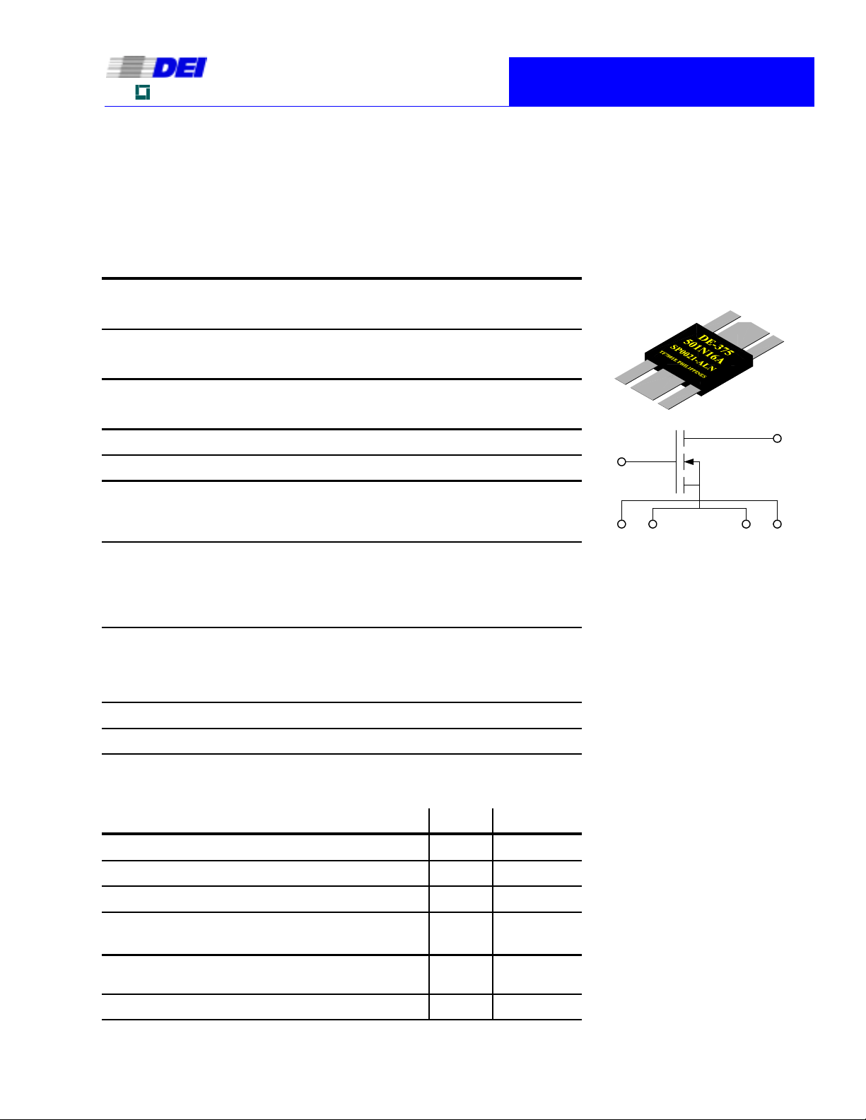
GATE
SG1 SG2
Features
•
Isolated Substrate
−
high isolation voltage (>2500V)
−
excellent thermal transfer
−
Increased temperature and power
cycling capability
•
IXYS advanced low Qg process
•
Low gate charge and capacitances
−
easier to drive
−
faster switching
•
Low R
•
Very low insertion inductance (<2nH)
•
No beryllium oxide (BeO) or other
hazardous materials
Advantages
•
Optimized for RF and high speed
switching at frequencies to 100MHz
•
Easy to mount—no insulators needed
•
High power density
DS(on)
.5 ΩΩΩΩ
DRAIN
SD1 SD2
g
fs
VDS = 15 V, ID = 0.5I
, pulse test
D25
2 6 S
Page 2
Directed Energy, Inc.
An
IXYS
Symbol Test Conditions Characteristic Values
Company
TJ = 25°C unless otherwise specified)
(
DE275-501N16A
RF Power MOSFET
R
C
C
C
T
T
T
T
Q
Q
Q
G
iss
oss
rss
d(on)
on
d(off)
off
g(on)
gs
gd
1800 pF
VGS = 0 V, VDS = 0.8 V
f = 1 MHz
VGS = 15 V, VDS = 0.8 V
ID = 0.5 IDM
R
= 0.2 Ω (External)
G
VGS = 10 V, VDS = 0.5 V
ID = 0.5 I
D25
DSS(max)
DSS
DSS
min. typ. max.
,
150 pF
0.3
45 pF
3 ns
2 ns
4 ns
5 ns
50 nC
20 nC
30 nC
Ω
Source-Drain Diode Characteristic Values
TJ = 25°C unless otherwise specified)
(
Symbol Test Conditions min. typ. max.
I
S
I
SM
V
SD
T
rr
Q
RM
I
RM
VGS = 0 V
Repetitive; pulse width limited by T
IF = IS, VGS = 0 V,
Pulse test, t ≤ 300 µs, duty cycle ≤ 2%
IF = I
, -di/dt = 100A/µs,
S
V
= 100V
R
JM
4 A
6 A
48 A
1.5 V
200 ns
0.6
µC
Directed Energy, Inc. reserves the right to change limits, test conditions and dimensions.
DEI MOSFETS are covered by one or more of the following U.S. patents:
4,835,592 4,850,072 4,881,106 4,891,686 4,931,844 5,017,508
5,034,796 5,049,961 5,063,307 5,187,117 5,237,481 5,486,715
5,381,025 5,640,045
Page 3
An
IXYS
Directed Energy, Inc.
Company
DE275-501N16A
RF Power MOSFET
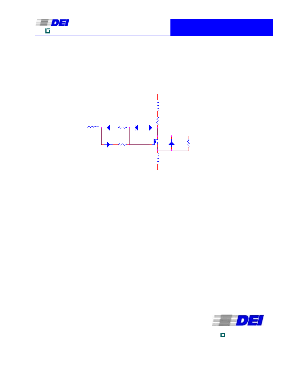
501N16A DE-SERIES SPICE Model
The DE-SERIES SPICE Model is illustrated in Figure 1. The model is an expansion of the SPICE
level 3 MOSFET model. It includes the stray inductive terms L
the device, Rds is the resistive leakage term. The output capacitance, C
capacitance, C
are modeled with reversed biased diodes. This provides a varactor type re-
RSS
sponse necessary for a high power device model. The turn on delay and the turn off delay are adjusted via Ron and Roff.
, LS and LD. Rd is the R
G
, and reverse transfer
OSS
DS(ON)
of
10 DRAIN
Ld
20 GATE
Doff
Lg
5678
Roff
Ron
Don
D1crs
D2crs
4
2
30 SOURCE
Rd
13
Dcos
M3
Ls
Rds
Figure 1 DE-SERIES SPICE Model
This SPICE model may be downloaded as a text file from the DEI web site at
www.directedenergy.com/spice.htm
Net List:
SYM=POWMOSN
.SUBCKT 501N16A 10 20 30
* TERMINALS: D G S
* 500 Volt 16 Amp .5 ohm N-Channel Power MOSFET
* REVA 6-15-00
M1 1 2 3 3 DMOS L=1U W=1U
RON 5 6 .2
DON 6 2 D1
ROF 5 7 .2
DOF 2 7 D1
D1CRS 2 8 D2
D2CRS 1 8 D2
CGS 2 3 2.0N
RD 4 1 .5
DCOS 3 1 D3
RDS 1 3 5.0MEG
LS 3 30 .5N
LD 10 4 1N
LG 20 5 1N
.MODEL DMOS NMOS (LEVEL=3 VTO=3.0 KP=5.8)
.MODEL D1 D (IS=.5F CJO=10P BV=100 M=.5 VJ=.7 TT=1N RS=10M)
.MODEL D2 D (IS=.5F CJO=450P BV=500 M=.4 VJ=.6 TT=10N RS=10M)
.MODEL D3 D (IS=.5F CJO=900P BV=500 M=.3 VJ=.3 TT=400N RS=10M)
.ENDS
Doc #9200-0222 Rev 1
© 2001 Directed Energy, Inc.
Directed Energy, Inc.
An
2401 Research Blvd., Suite 108
Fort Collins, CO USA 80526
970-493-1901 Fax: 970-493-1903
Email: deiinfo@directedenergy.com
Web: http://www.directedenergy.com
IXYS Company
 Loading...