

Datasheet DAC1600KP-V, DAC1600JP-V, DAC703SH, DAC703LH, DAC703KP Datasheet (Burr Brown Corporation)
...Page 1
1
®
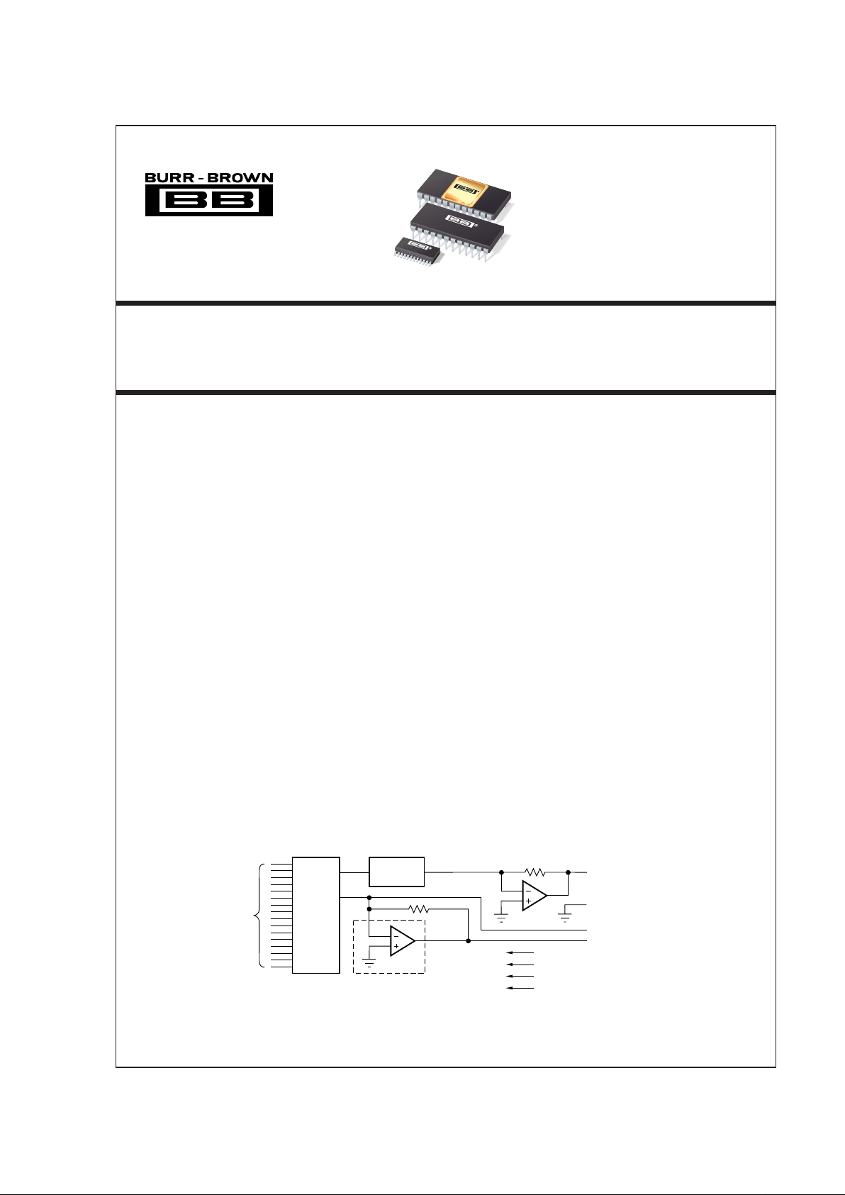
DAC701, 702, 703
Monolithic 16-Bit
DIGITAL-TO-ANALOG CONVERTERS
FEATURES
● V
OUT
AND I
OUT
MODELS
● HIGH ACCURACY:
Linearity Error
±0.0015% of FSR max
Differential Linearity Error
±0.003% of FSR
max
DAC701
DAC702
DAC703
®
16-Bit
Ladder
Resistor
Network
And
Current
Switches
Digital
Inputs
Reference
Circuit
Reference Output
Summing Junction
Output
Common
Gain Adjust
+V
–V
V
CC
CC
DD
Voltage Models
Only
International Airport Industrial Park • Mailing Address: PO Box 11400, Tucson, AZ 85734 • Street Address: 6730 S. Tucson Blvd., Tucson, AZ 85706 • Tel: (520) 746-1111 • Twx: 910-952-1111
Internet: http://www.burr-brown.com/ • FAXLine: (800) 548-6133 (US/Canada Only) • Cable: BBRCORP • Telex: 066-6491 • FAX: (520) 889-1510 • Immediate Product Info: (800) 548-6132
● MONOTONIC (at 15 bits) OVER FULL
SPECIFICATION TEMPERATURE RANGE
● PIN-COMPATIBLE WITH DAC70, DAC71,
DAC72
● DUAL-IN-LINE PLASTIC AND HERMETIC
CERAMIC AND SOIC
DESCRIPTION
The DAC70X family comprise of complete 16-bit
digital-to-analog converters that includes a precision
buried-zener voltage reference and a low-noise, fastsettling output operational amplifier (voltage output
models), all on one small monolithic chip. A combination of current-switch design techniques accomplishes
not only 15-bit monotonicity over the entire specified
temperature range, but also a maximum end-point
linearity error of ±0.0015% of full-scale range. Total
full-scale gain drift is limited to ±10ppm/°C maximum
(LH and CH grades).
Digital inputs are complementary binary coded and
are TTL-, LSTTL-, 54/74C- and 54/74HC-compatible
over the entire temperature range. Outputs of 0 to
+10V, ±10V, 0 to –2mA, and ±1mA are available.
These D/A converters are packaged in hermetic 24-pin
ceramic side-brazed or molded plastic. The DIP-packaged parts are pin-compatible with the voltage and
current output DAC71 and DAC72 model families.
The DAC702 is also pin-compatible with the DAC70
model family. In addition, the DAC703 is offered in a
24-pin SOIC package for surface mount applications.
© 1983 Burr-Brown Corporation PDS-494M Printed in U.S.A. March, 1998
DAC701
DAC702
DAC703
Page 2

2
®
DAC701, 702, 703
SPECIFICATIONS
At +25°C and rated power supplies, unless otherwise noted.
DAC702/703J DAC701/702/703K DAC701/702/703B, S DAC701/702/703L, C
PARAMETER MIN TYP MAX MIN TYP MAX MIN TYP MAX MIN TYP MAX UNITS
INPUT
DIGITAL INPUT
Resolution 16 ✻✻✻Bits
Digital Inputs
(1)
V
IH
+2.4 +V
CC
✻✻✻✻✻✻V
V
IL
–1.0 +0.8 ✻✻✻✻✻✻V
I
IH
, VI = +2.7V +40 ✻✻✻µA
I
IL
, VI = +0.4V –0.35 –0.5 ✻ ✻ ✻✻ ✻✻ mA
TRANSFER CHARACTERISTICS
ACCURACY
(2)
Linearity Error
(4)
±0.0015 ±0.006 ✻ ±0.003 ✻✻ ±0.00075 ±0.0015 % of FSR
(3)
Differential Linearity
Error
(4)
±0.003 ±0.012 ✻ ±0.006 ✻✻ ±0.0015 ±0.003 % of FSR
Differential Linearity
Error at Bipolar Zero
(DAC702/703)
(4)
±0.003 ±0.006 ±0.0015 ±0.003 ✻✻% of FSR
Gain Error
(5)
±0.07 ±0.30 ✻ ±0.15 ±0.05 ±0.10 ✻✻ %
Zero Error
(5, 6)
±0.05 ±0.10 ✻ ✻ ✻✻ ✻✻% of FSR
Monotonicity Over Spec.
Temp Range 13 14 ✻ 15 Bits
DRIFT (over specification
temperature range)
Total Error Over
Temperature Range
(all models)
(7)
±0.08 ✻ ±0.15 ±0.05 ±0.10 ✻✻% of FSR
Total Full Scale Drift:
DAC701 ±10 ✻ ±30 ±8.5 ±18 ±6 ±13 ppm of FSR/°C
DAC702/703 ±10 ✻ ±25 ±7 ±15 ✻✻ppm of FSR/°C
Gain Drift (all models) ±10 ±30 ✻ ±25 ±7 ±15 ±5 ±10 ppm/°C
Zero Drift:
DAC701 ±2.5 ±5 ±1.5 ±3 ✻✻ppm of FSR/°C
DAC702/703 ±5 ±15 ✻ ±12 ±4 ±10 ±2.5 ±5 ppm of FSR/°C
Differential Linearity
Over Temp.
(4)
±0.012 +0.009, ✻ +0.006, % of FSR
–0.006 –0.003
Linearity Error
Over Temp.
(4)
±0.012 ±0.006 ✻ ±0.003 % of FSR
SETTLING TIME (to
±0.003% of FSR)
(8)
DAC701/703 (V
OUT
Models)
Full Scale Step, 2kΩ Load 4 ✻ 8 ✻✻ ✻✻ µs
1LSB Step at
Worst-Case Code
(9)
2.5 ✻✻✻µs
Slew Rate 10 ✻✻✻V/µs
DAC702 (I
OUT
Models)
Full Scale Step (2mA),
10 to 100Ω Load 350 ✻ 1000 ✻✻ ✻✻ ns
1kΩ Load 1 ✻ 3 ✻✻ ✻✻ µs
OUTPUT
VOLTAGE OUTPUT
MODELS
DAC701 (CSB Code) 0 to +10 ✻ V
DAC703 (COB Code) ±10 ✻✻✻V
Output Current ±5 ✻✻✻ mA
Output Impedance 0.15 ✻✻✻Ω
Short Circuit to
Common Duration Indefinite ✻✻✻
CURRENT OUTPUT
MODELS
DAC702 (COB Code)
(10)
±1 ✻✻✻mA
Output Impedance
(10)
2.45 ✻✻✻kΩ
Compliance Voltage ±2.5 ✻✻✻V
Page 3
3
®
DAC701, 702, 703
The information provided herein is believed to be reliable; however, BURR-BROWN assumes no responsibility for inaccuracies or omissions. BURR-BROWN assumes no
responsibility for the use of this information, and all use of such information shall be entirely at the user’s own risk. Prices and specifications are subject to change without notice.
No patent rights or licenses to any of the circuits described herein are implied or granted to any third party. BURR-BROWN does not authorize or warrant any BURR-BROWN
product for use in life support devices and/or systems.
DAC702/703J DAC701/702/703K DAC701/702/703B, S DAC701/702/703L, C
PARAMETER MIN TYP MAX MIN TYP MAX MIN TYP MAX MIN TYP MAX UNITS
REFERENCE VOLTAGE
Voltage +6.3 +6.0 +6.3 +6.6 +6.24 +6.3 +6.36 ✻✻✻ V
Source Current Available
for External Loads +2.5 +1.5 ✻✻✻✻✻ mA
Temperature Coefficient ±10 ✻ ±25 ✻ ±15 ✻✻ ppm/°C
Short Circuit to Common
Duration Indefinite ✻✻✻
POWER SUPPLY REQUIREMENTS
Voltage: +V
CC
13.5 15 16.5 ✻✻✻✻✻✻✻✻✻ V
–V
CC
13.5 15 16.5 ✻✻✻✻✻✻✻✻✻ V
V
DD
+4.5 +5 +16.5 ✻✻✻✻✻✻✻✻✻ V
Current (No Load):
DAC702
(I
OUT
Models)
+V
CC
+10 +25 ✻✻ ✻✻ ✻✻ mA
–V
CC
–13 –25 ✻✻ ✻✻ ✻✻ mA
V
DD
+4 +8 ✻✻ ✻✻ ✻✻ mA
DAC701/703
(V
OUT
Models)
+V
CC
+16 +30 ✻✻ ✻✻ ✻✻ mA
–V
CC
–18 –30 ✻✻ ✻✻ ✻✻ mA
V
DD
+4 +8 ✻✻ ✻✻ ✻✻ mA
Power Dissipation:
(V
DD
= +5.0V)
(11)
DAC702 365 ✻ 790 ✻ 630 ✻✻ mW
DAC701/703 530 ✻ 940 ✻ 780 ✻✻ mW
Power Supply Rejection:
+V
CC
±0.0015 ±0.006 ✻✻ ✻±0.003 ✻✻% of FSR/%V
CC
–V
CC
±0.0015 ±0.006 ✻✻ ✻±0.003 ✻✻% of FSR/%V
CC
V
DD
±0.0001 ±0.001 ✻✻ ✻✻ ✻✻% of FSR/%V
DD
TEMPERATURE RANGE
Specification:
B, C Grades –25 +85 ✻✻°C
S Grades –55 +125 °C
J, K, L Grades 0 +70 ✻✻ 0 +70 °C
Storage: Ceramic –60 +150 ✻✻✻✻°C
Plastic, SOIC –60 +100 ✻✻ °C
✻ Specification same as model to the left.
NOTES: (1) Digital inputs are TTL, LSTTL, 54/74C, 54/74HC, and 54/74HTC compatible over the operating voltage range of V
DD
= +5V to +15V and over the specified
temperature range. The input switching threshold remains at the TTL threshold of 1.4V over the supply range of V
DD
= +5V to +15V. As logic “0” and logic “1” inputs vary over
0V to +0.8V and +2.4V to +10V respectively, the change in the D/A converter output voltage will not exceed ±0.0015% of FSR for the LH and CH grades, ±0.003% of FSR for
the BH grade and ±0.006% of FSR for the KG grade. (2) DAC702 (current-output models) is specified and tested with an external output operational amplifier connected using
the internal feedback resistor in all parameters except settling time. (3) FSR means full-scale range and is 20V for the ±10V range (DAC703), 10V for the 0 to +10V range
(DAC701). FSR is 2mA for the ±1mA range (DAC702). (4) ±0.0015% of full-scale range is equivalent to 1LSB in 15-bit resolution. ±0.003% of full-scale range is equivalent to
1LSB in 14-bit resolution. ±0.006% of full-scale range is equivalent to 1LSB in 13-bit resolution. (5) Adjustable to zero with external trim potentiometer. Adjusting the gain
potentiometer rotates the transfer function around the zero point. (6) Error at input code FFFF
H
for DAC701, 7FFFH for DAC702 and DAC703. (7) With gain and zero errors
adjusted to zero at +25°C. (8) Maximum represents the 3σ limit. Not 100% tested for this parameter. (9) At the major carry, 7FFF
H
to 8000H and 8000H to 7FFFH. (10) Tolerance
on output impedance and output current is ±30%. (11) Power dissipation is an additional 40mW when V
DD
is operated at +15V.
SPECIFICATIONS (CONT)
At +25°C and rated power supplies, unless otherwise noted.
Page 4

4
®
DAC701, 702, 703
CONNECTION DIAGRAMS
–V
1
2
3
4
5
6
7
8
9
10
11
12
24
23
22
21
20
19
18
17
16
15
14
13
MSB
16-Bit
Ladder
Resistor
Network
and
Current
Switches
Digital
Inputs
Reference
Circuit
R
F
(4)
Voltage Models
Only
LSB
Digital
Inputs
(2)
+V
CC
270kΩ
3.9MΩ
(3)
(3)
0.0022µF
(2)
(2)
V
DD
CC
(1)
NOTES: (1) Can be tied to +VCC instead of having
separate V
DD
supply. (2) Decoupling capacitors are
0.1µF to 1.0µF. (3) Potentiometers are 10kΩ to
100kΩ. (4) 5kΩ (DAC701), 10kΩ (DAC702/703).
ALL PACKAGES
PIN # DAC702 DAC701/703
1 Bit 1 (MSB) Bit 1 (MSB)
2 Bit 2 Bit 2
3 Bit 3 Bit 3
4 Bit 4 Bit 4
5 Bit 5 Bit 5
6 Bit 6 Bit 6
7 Bit 7 Bit 7
8 Bit 8 Bit 8
9 Bit 9 Bit 9
10 Bit 10 Bit 10
11 Bit 11 Bit 11
12 Bit 12 Bit 12
13 Bit 13 Bit 13
14 Bit 14 Bit 14
15 Bit 15 Bit 15
16 Bit 16 (LSB) Bit 16 (LSB)
17 R
FEEDBACK
V
OUT
18 V
DD
V
DD
19 –V
CC
–V
CC
20 Common Common
21 I
OUT
Summing Junction (Zero Adjust)
22 Gain Adjust Gain Adjust
23 +V
CC
+V
CC
24 +6.3V Reference Output +6.3V Reference Output
ABSOLUTE MAXIMUM RATINGS
(1)
+VCC to Common ........................................................................ 0V, +18V
–V
CC
to Common ........................................................................ 0V, –18V
V
DD
to Common .......................................................................... 0V, +18V
Digital Data Inputs to Common ................................................ –1V, +18V
Reference Out to Common ........................... Indefinite Short to Common
External Voltage Applied to R
F
(DAC702) ......................................... ±18V
External Voltage Applied to D/A Output (DAC701/703).......... –5V to +5V
V
OUT
(DAC701/703) .......................................Indefinite Short to Common
Power Dissipation .................................................................................1W
Storage Temperature ...................................................... –60°C to +150°C
Lead Temperature (soldering, 10s) ................................................. 300°C
NOTE: (1) Stresses above those listed under “Absolute Maximum Ratings”
may cause permanent damage to the device. Exposure to absolute maximum
conditions for extended periods may affect device reliability.
PIN ASSIGNMENTS
ELECTROSTATIC
DISCHARGE SENSITIVITY
This integrated circuit can be damaged by ESD. Burr-Brown
recommends that all integrated circuits be handled with
appropriate precautions. Failure to observe proper handling
and installation procedures can cause damage.
ESD damage can range from subtle performance degradation to complete device failure. Precision integrated circuits
may be more susceptible to damage because very small
parametric changes could cause the device not to meet its
published specifications.
Page 5

5
®
DAC701, 702, 703
PACKAGE/ORDERING INFORMATION
LINEARITY GAIN
PACKAGE ERROR, MAX DRIFT,
DRAWING OUTPUT TEMPERATURE AT+25
°C MAX
PRODUCT PACKAGE NUMBER
(1)
CONFIGURATION RANGE (% of FSR) (ppm/°C)
DAC703JP 24-Pin Plastic DIP 167 ±1mA, ±10V 0°C to +70°C ±0.006 ±30
DAC703KP 24-Pin Plastic DIP 167 ±1mA, ±10V 0°C to +70°C ±0.003 ±25
DAC701KH 24-Pin Ceramic DIP 165 0 to –2mA, 0 to +10V 0°C to +70°C ±0.003 ±25
DAC702KH 24-Pin Ceramic DIP 165 ±1mA, ±10V 0°C to +70°C ±0.003 ±25
DAC703KH 24-Pin Ceramic DIP 165 ±1mA, ±10V 0°C to +70°C ±0.003 ±25
DAC701BH 24-Pin Ceramic DIP 165 0 to –2mA, 0 to +10V –25°C to +85°C ±0.003 ±15
DAC702BH 24-Pin Ceramic DIP 165 ±1mA, ±10V –25°C to +85°C ±0.003 ±15
DAC703BH 24-Pin Ceramic DIP 165 ±1mA, ±10V –25°C to +85°C ±0.003 ±15
DAC701LH 24-Pin Ceramic DIP 165 0 to –2mA, 0 to +10V 0°C to +70°C ±0.0015 ±10
DAC702LH 24-Pin Ceramic DIP 165 ±1mA, ±10V 0°C to +70°C ±0.0015 ±10
DAC703LH 24-Pin Ceramic DIP 165 ±1mA, ±10V 0°C to +70°C ±0.0015 ±10
DAC701CH 24-Pin Ceramic DIP 165 0 to –2mA, 0 to +10V –25°C to +85°C ±0.0015 ±10
DAC702CH 24-Pin Ceramic DIP 165 ±1mA, ±10V –25°C to +85°C ±0.0015 ±10
DAC703CH 24-Pin Ceramic DIP 165 ±1mA, ±10V –25°C to +85°C ±0.0015 ±10
DAC701SH 24-Pin Ceramic DIP 165 0 to –2mA, 0 to +10V –55°C to +125°C ±0.003 ±15
DAC702SH 24-Pin Ceramic DIP 165 ±1mA, ±10V –55°C to +125°C ±0.003 ±15
DAC703SH 24-Pin Ceramic DIP 165 ±1mA, ±10V –55°C to +125°C ±0.003 ±15
DAC703JU 24-Pin SOIC 239 ±10V 0°C to +70°C ±0.006 ±30
DAC703KU 24-Pin SOIC 239 ±10V 0°C to +70°C ±0.003 ±25
NOTE: (1) For detailed drawing and dimension table, please see end of data sheet, or Appendix C of Burr-Brown IC Data Book.
Page 6

6
®
DAC701, 702, 703
DISCUSSION OF
SPECIFICATIONS
DIGITAL INPUT CODES
The DAC701/702/703 accept complementary digital
input codes in either binary format (CSB, unipolar or
COB, bipolar). The COB models DAC702/703 may be
connected by the user for either complementary offset
binary (COB) or complementary two’ s complement (CTC )
codes (see Table I).
Zero Drift
Zero drift is a measure of the change in the output with
FFFF
H
(DAC701) applied to the digital inputs over the
specified temperature range. For the bipolar models, zero is
measured at 7FFFH (bipolar zero) applied to the digital
inputs. This code corresponds to zero volts (DAC703) or
zero milliamps (DAC702) at the analog output. The maximum change in offset at t
MIN
or t
MAX
is referenced to the
zero error at +25°C and is divided by the temperature
change. This drift is expressed in parts per million of full
scale range per degree centigrade (ppm of FSR/°C).
SETTLING TIME
Settling time of the D/A is the total time required for the
analog output to settle within an error band around its final
value after a change in digital input. Refer to Figure 1 for
typical values for this family of products.
Voltage Output
Settling times are specified to ±0.003% of FSR (±1/2LSB
for 14 bits) for two input conditions: a full-scale range
change of 20V (DAC703) or 10V (DAC701) and a 1LSB
change at the “major carry,” the point at which the worstcase settling time occurs. (This is the worst-case point since
all of the input bits change when going from one code to the
next).
Current Output
Settling times are specified to ±0.003% of FSR for a fullscale range change for two output load conditions: one for
10Ω to 100Ω and one for 1000Ω. It is specified this way
because the output RC time constant becomes the dominant
factor in determining settling time for large resistive loads.
ANALOG OUTPUT
DAC701 DAC702/703 DAC702/703
DIGITAL Complementary Complementary Complementary
INPUT Straight Binary Offset Binary Two’s Complement
CODES (CSB) (COB) (CTC)*
0000
H
+ Full Scale + Full Scale –1LSB
7FFF
H
+1/2 Full Scale Bipolar Zero – Full Scale
8000
H
+1/2 Full Scale –1LSB + Full Scale
–1LSB
FFFF
H
Zero – Full Scale Bipolar Zero
* Invert the MSB of the COB code with an external inverter to obtain CTC
code.
TABLE I. Digital Input Codes.
ACCURACY
Linearity
This specification describes one of the most important measures of performance of a D/A converter. Linearity error is
the deviation of the analog output from a straight line drawn
through the end points (all bits ON point and all bits OFF
point).
Differential Linearity Error
Differential linearity error (DLE) of a D/A converter is the
deviation from an ideal 1LSB change in the output from one
adjacent output state to the next. A differential linearity error
specification of ±1/2LSB means that the output step sizes
can be between 1/2LSB and 3/2LSB when the input changes
from one adjacent input state to the next. A negative DLE
specification of no more than –1LSB (–0.006% for 14-bit
resolution) insures monotonicity.
Monotonicity
Monotonicity assures that the analog output will increase or
remain the same for increasing input digital codes. The
DAC701/702/703 are specified to be monotonic to 14 bits
over the entire specification temperature range.
DRIFT
Gain Drift
Gain drift is a measure of the change in the full-scale range
output over temperature expressed in parts per million per
degree centigrade (ppm/°C). Gain drift is established by: (1)
testing the end point differences for each D/A at t
MIN
, +25°C
and t
MAX
; (2) calculating the gain error with respect to the
+25°C value; and (3) dividing by the temperature change.
FIGURE 1. Final-Value Error Band vs Full-Scale Range
Settling Time.
COMPLIANCE VOLTAGE
Compliance voltage applies only to current output models. It
is the maximum voltage swing allowed on the output current
pin while still being able to maintain specified accuracy.
Final-Value Error Band, Percent of
Full-Scale Range (±% of FSR)
Settling Time (µs)
0.01 0.1 1 10
1
0.1
0.01
0.001
DAC702
DAC701
DAC703
RL = 100Ω
R
L
= 1kΩ
Page 7

7
®
DAC701, 702, 703
POWER SUPPLY SENSITIVITY
Power supply sensitivity is a measure of the effect of a
change in a power supply voltage on the D/A converter
output. It is defined as a percent of FSR change in the output
per percent of change in either the positive supply (+VCC),
negative supply (–V
CC
) or logic supply (VDD) about the
nominal power supply voltages (see Figure 2).
It is specified for DC or low frequency changes. The typical
performance curve in Figure 2 shows the effect of high
frequency changes in power supply voltages.
FIGURE 2. Power Supply Rejection vs Power Supply Ripple
Frequency.
Power Supply Ripple Frequency (Hz)
1 10 100 1k 10k 100k
0.030
0.025
0.020
0.015
0.01
0.005
0
% of FSR Error Per % of Change in V
SUPPLY
–15V Supply
+15V
Supply
+5V
Supply
REFERENCE SUPPLY
All models have an internal low-noise +6.3V reference
voltage derived from an on-chip buried zener diode. This
reference voltage, available to the user, has a tolerance of
±5% (KH models) and ±1% (BH models). A minimum of
1.5mA is available for external loads. Since the output
impedance of the reference output is typically 1W, the
external load should remain constant.
If a varying load is to be driven by the reference supply, an
external buffer amplifier is recommended to drive the load
in order to isolate the bipolar offset (connected internally to
the reference) from load variations.
OPERATING INSTRUCTIONS
POWER SUPPLY CONNECTIONS
For optimum performance and noise rejection, power supply decoupling capacitors should be added as shown in the
Connection Diagram. 1µF tantalum capacitors should be
located close to the D/A converter.
EXTERNAL ZERO AND GAIN ADJUSTMENT
Zero and gain may be trimmed by installing external zero
and gain potentiometers. Connect these potentiometers as
shown in the Connection Diagram and adjust as described
below. TCR of the potentiometers should be 100ppm/°C or
less. The 3.9MΩ and 270kΩ resistors (±20% carbon or
better) should be located close to the D/A converter to
prevent noise pickup. If it is not convenient to use these
high-value resistors, an equivalent “T” network, as shown in
Figure 3, may be substituted in place of the 3.9MΩ part. A
0.001µF to 0.01µF ceramic capacitor should be connected
from Gain Adjust to Common to prevent noise pickup. Refer
to Figures 4 and 5 for the relationship of zero and gain
adjustments to unipolar and bipolar D/A converters.
FIGURE 3. Equivalent Resistances.
≡
180kΩ 180kΩ3.9MΩ
10kΩ
Digital Input
H
Input =
0000
H
Input =
FFFF
Gain Adjust
Rotates
the Line
Range
of Gain
Adjust
1LSB
+ Full
Scale
Full Scale Range
Range of
Zero Adjust
Zero Adjust
Translates
the Line
Analog Output
FIGURE 4.
Relationship of Zero and Gain Adjustments for
Unipolar D/A Converters, DAC701.
Digital Input
H
Input =
FFFF
Gain
Adjust
Rotates
the Line
Range
of Gain
Adjust
1LSB
Full Scale
Range
+ Full
Scale
– Full
Scale
Range
and
Offset
Adjust
Offset
Adjust
Translates
the Line
H
Input =
0000
MSB on All
Others Off 7FFF
H
Analog Output
FIGURE 5. Relationship of Zero and Gain Adjustments for
Bipolar D/A Converters, DAC702 and DAC703.
Page 8

8
®
DAC701, 702, 703
In many applications it is impractical to sense the output
voltage at the output pin. Sensing the output voltage at the
system ground point is permissible with the DAC700 family
because the D/A converter is designed to have a constant
return current of approximately 2mA flowing from Common. The variation in this current is under 20µA (with
changing input codes), therefore R4 can be as large as 3Ω
without adversely affecting the linearity of the D/A converter. The voltage drop across R4 (R4 x 2mA) appears as a
zero error and can be removed with the zero calibration
adjustment. This alternate sensing point (the system ground
point) is shown in Figures 6, 7, and 8.
Figures 7 and 8 show two methods of connecting the current
output models (DAC702) with external precision output op
amps. By sensing the output voltage at the load resistor (ie,
by connecting R
F
to the output of A1 at RL), the effect of R
1
and R2 is greatly reduced. R1 will cause a gain error but is
independent of the value of R
L
and can be eliminated by
initial calibration adjustments. The effect of R
2
is negligible
because it is inside the feedback loop of the output op amp
and is therefore greatly reduced by the loop gain.
Zero Adjustment
For unipolar (CSB) configurations, apply the digital input
code that produces zero voltage or zero current output and
adjust the zero potentiometer for zero output.
For bipolar (COB, CTC) configurations, apply the digital
input code that produces zero output voltage or current. See
Table II for corresponding codes and the Connection Diagram for zero adjustment circuit connections. Zero calibration should be made before gain calibration.
Gain Adjustment
Apply the digital input that gives the maximum positive
output voltage. Adjust the gain potentiometer for this positive full scale voltage. See Table II for positive full scale
voltages and the Connection Diagram for gain adjustment
circuit connections.
INSTALLATION
CONSIDERATIONS
This D/A converter family is laser-trimmed to 14-bit linearity. The design of the device makes the 16-bit resolution
available. If 16-bit resolution is not required, bit 15 and bit
16 should be connected to V
DD
through a single 1kΩ
resistor.
Due to the extremely high resolution and linearity of the
D/A converter, system design problems such as grounding
and contact resistance become very important. For a 16-bit
converter with a 10V full-scale range, 1LSB is 153µV. With
a load current of 5mA, series wiring and connector resistance of only 30mΩ will cause the output to be in error by
1LSB. To understand what this means in terms of a system
layout, the resistance of #23 wire is about 0.021Ω/ft. Neglecting contact resistance, less than 18 inches of wire will
produce a 1LSB error in the analog output voltage!
In Figures 6, 7, and 8, lead and contact resistances are
represented by R
1
through R5. As long as the load resistance
R
L
is constant, R2 simply introduces a gain error and can be
removed during initial calibration. R
3
is part of RL, if the
output voltage is sensed at Common, and therefore introduces no error. If RL is variable, then R2 should be less than
R
L MIN
/216 to reduce voltage drops due to wiring to less than
1LSB. For example, if R
L MIN
is 5kΩ, then R2 should be less
than 0.08Ω. R
L
should be located as close as possible to the
D/A converter for optimum performance. The effect of R
4
is
negligible.
FIGURE 6. Output Circuit for Voltage Models.
A
1
R
DAC
4kΩ
DAC701
5kΩ
R
B
Common
V
OUT
R
2
*
R
L
R
3
Sense Output
+5VDC
Supply
±15VDC
Supply
+V
COM
–V
System Ground
Point
+V
COM
Alternate Ground
Sense Connection
R
4
To +V
CC
To –V
CC
To V
DD
1µF
1µF
1µF
* R = 2k (DAC701 and DAC703)
B
Ω
R
F
Page 9

9
®
DAC701, 702, 703
VOLTAGE OUTPUT MODELS
ANALOG OUTPUT
DAC701 UNIPOLAR DAC703 BIPOLAR
DIGITAL INPUT CODE 16-BIT 15-BIT 14-BIT 16-BIT 15-BIT 14-BIT
1LSB (µV) 153 305 610 305 610 1224
0000
H
(V) +9.99985 +9.99969 +9.99939 +9.99960 +9.99939 +9.99878
FFFF
H
(V) 0 0 0 –10.0000 –10.0000 –10.0000
ANALOG OUTPUT MODEL
ANALOG OUTPUT
DAC702 BIPOLAR
DIGITAL INPUT CODE 16-BIT 15-BIT 14-BIT
1LSB (µA) 0.031 0.061 0.122
0000
H
(mA) –0.99997 –0.99994 –0.99988
FFFF
H
(mA) +1.00000 +1.00000 +1.00000
TABLE II. Digital Input and Analog Output Relationships.
If the output cannot be sensed at Common or the system
ground point as mentioned above, the differential output
circuit shown in Figure 8 is recommended. In this circuit the
output voltage is sensed at the load common and not at the
D/A converter common as in the previous circuits. The value
of R
6
and R7 must be adjusted for maximum common-mode
rejection at R
L
. Note that if R3 is negligible, the circuit of
Figure 8 can be reduced to the one shown in Figure 7. Again
the effect of R4 is negligible.
The D/A converter and the wiring to its connectors should be
located to provide optimum isolation from sources of RFI
and EMI. The key concept in elimination of RF radiation or
pickup is loop area; therefore, signal leads and their return
conductors should be kept close together. This reduces the
external magnetic field along with any radiation. Also, if a
single lead and its return conductor are wired close together,
they present a small flux-capture cross section for any
external field. This reduces radiation pickup in the circuit.
FIGURE 7. Preferred External Op Amp Configuration. FIGURE 8. Differential Sensing Output Op Amp
Configuration.
A
1
R
DAC
DAC702
R
B
Common
I
OUT
R
1
‡
R
L
R
3
Sense Output
+5VDC
Supply
±15VDC
Supply
+V
COM
–V
System Ground
Point
+V
COM
Alternate Ground
Sense Connection
R
4
To +V
CC
To –V
CC
To V
DD
1µF
1µF
1µF
*
2.45k
R
F
*
R
2
R should be equal to the output impedance at the current output
to compensate for the bias current drift of A . Use standard 10%,
1/4W carbon composition or equivalent resistors.
B
1
‡
DAC702
Ω
2.45k
10k
ΩΩ
R
DAC
R
B
R
F
*
R
F
A
1
R
DAC
DAC702
R
6
Common
I
OUT
R
1
R
L
R
3
+5VDC
Supply
±15VDC
Supply
+V
COM
–V
System Ground
Point
+V
COM
Alternate Ground
Sense Connection
R
4
To +V
CC
To –V
CC
To V
DD
1µF
1µF
1µF
2.45k
R
F
*
R
2
DAC702
Ω
10k
Ω
R
DAC
R
F
*
R
F
R
5
R
7
Sense
Output
+5R
7
R=+FR
1
R
R
6
=
DAC
R
Page 10

10
®
DAC701, 702, 703
APPLICATIONS
DRIVING AN EXTERNAL OP AMP
WITH CURRENT OUTPUT D/AS
DAC702 is current output devices and will drive the summing junction of an op amp to produce an output voltage as
shown in Figure 9. Use of the internal feedback resistor is
required to obtain specified gain accuracy and low gain drift.
DAC702 can be scaled for any desired voltage range with an
external feedback resistor, but at the expense of increased
drifts of up to ±50ppm/°C. The resistors in the DAC702 ratio
track to ±1ppm/°C but their absolute TCR may be as high as
±50ppm/°C.
An alternative method of scaling th e output voltage of the
D/A converter and preserving the low gain drift is shown in
Figure 10.
OUTPUTS LARGER THAN 20V RANGE
For output voltage ranges larger than ±10V, a high voltage
op amp may be employed with an external feedback resistor.
Use I
OUT
values of ±1mA for bipolar voltage ranges and
–2mA for unipolar voltage ranges (see Figure 11). Use
protection diodes as shown when a high voltage op amp is
used.
Common
I
OUT
V
OUT
R
F
5k
Ω
4k
Ω
0 to
2mA
FIGURE 9. External Op Amp Using Internal Feedback
Resistors.
I
OUT
V
OUT
R
F
5k
Ω
4k
Ω
0 to
2mA
R
1
I
*
R
2
*
Common
R
1
*, R2 TCR < ±10ppm/°C
FIGURE 10. External Op Amp Using Internal and External
Feedback Resistors to Maintain Low Gain Drift.
FIGURE 11. External Op Amp Using External Feedback
Resistors.
V
OUT
R
F
4k
Ω
0 to
2mA
BB3584
R
F
 Loading...